

Page 1
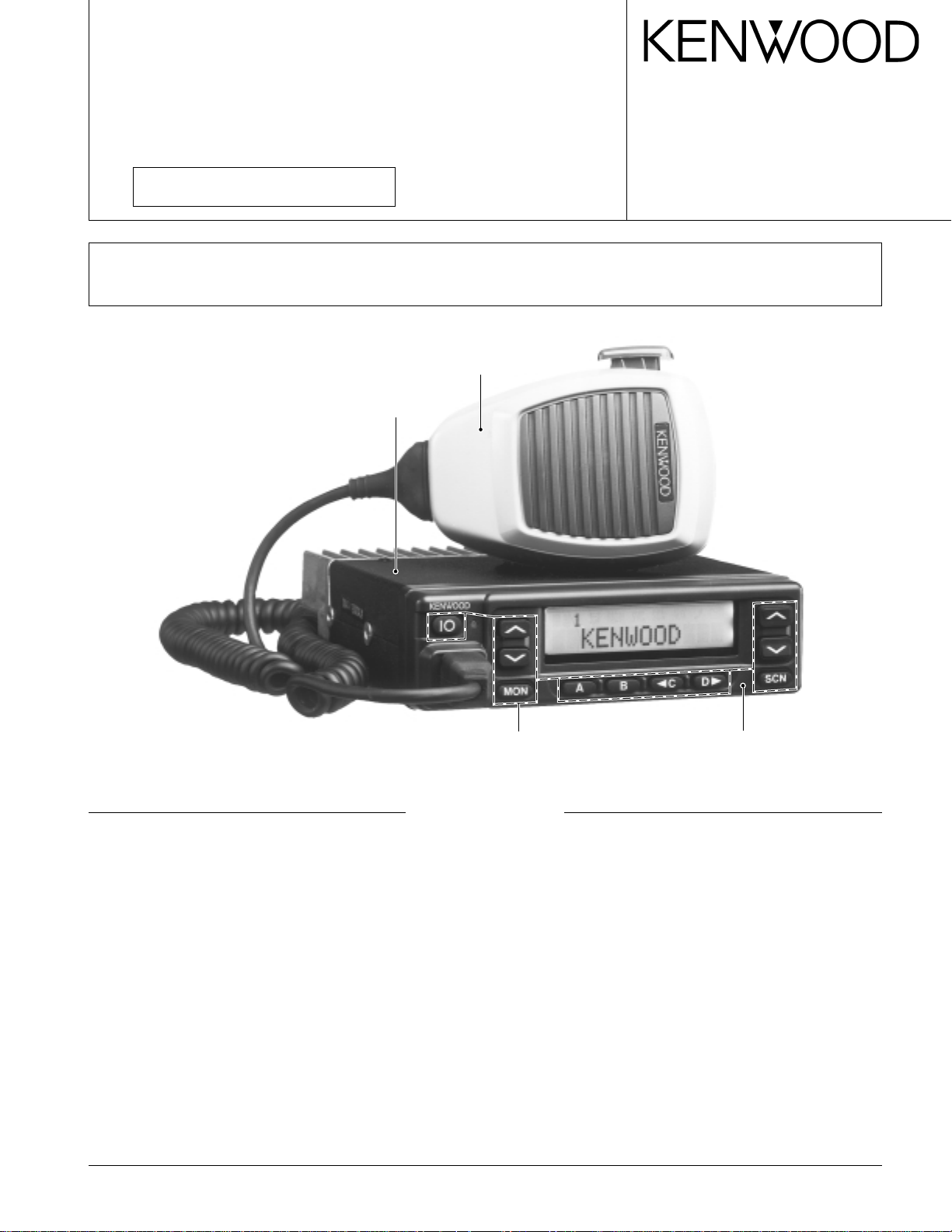
800MHz/900MHz FM TRANSCEIVER
TK-980/98 1
SERVICE MANUAL
SUPPLEMENT
This service manual applied to products with 30600001 or subsequent serial numbers.
In terms of the products with the serial numbers earlier than 30600001, refer to the TK-980/981 service manual as per
part No. B51-8478-10.
Microphone
(T91-0621-05)
Cabinet (Upper)
(A01-2165-23)
© 2001-9 PRINTED IN JAPAN
B51-8588-00 (N) 1016
CONTENTS
GENERAL ................................................................. 2
OPERATING FEATURES ......................................... 3
REALIGNMENT...................................................... 13
INSTALLATION...................................................... 16
CIRCUIT DESCRIPTION......................................... 25
SEMICONDUCTOR DATA..................................... 29
DESCRIPTION OF COMPONENTS ....................... 30
PARTS LIST ............................................................ 32
EXPLODED VIEW .................................................. 41
PACKING ................................................................ 42
Key top
(K29-5284-02)
ADJUSTMENT ....................................................... 43
PC BOARD VIEWS
PLL/VCO (X58-4530-XX) .................................. 50
TX-RX UNIT (X57-6520-XX) (A/2) ................... 51
TX-RX UNIT (X57-6520-XX) (B/2).................... 57
SCHEMATIC DIAGRAM ........................................ 61
BLOCK DIAGRAM.................................................. 69
LEVEL DIAGRAM................................................... 72
TERMINAL FUNCTION ......................................... 74
SPECIFICATIONS................................................... 75
Panel assy
(A62-0991-03)
Page 2

TK-980/98 1
GENERAL
INTRODUCTION
SCOPE OF THIS MANUAL
This manual is intended for use by experienced technicians familiar with similar types of commercial grade communications equipment. It contains all required service information for the equipment and is current as of the publication date. Changes which may occur after publication are
covered by either Service Bulletins or Manual Revisions,
which are issued as required.
ORDERING REPLACEMENT PARTS
When ordering replacement parts or equipment information, the full part identification number should be included.
This applies to all parts : components, kits, and chassis. If
the part number is not known, include the chassis or kit
number of which it is a part, and a sufficient description of
the required component for proper identification.
PERSONNEL SAFETY
The following precautions are recommended for personnel safety :
• DO NOT transmit if someone is within two feet (0.6
meter) of the antenna.
• DO NOT transmit until all RF connectors are secure and
any open connectors are properly terminated.
• SHUT OFF and DO NOT operate this equipment near
electrical blasting caps or in an explosive atmosphere.
• All equipment should be properly grounded before
power-up for safe operation.
• This equipment should be serviced by only qualified
technicians.
PRE-INSTALLATION CONSIDERNATIONS
1. UNPACKING
Unpack the radio from its shipping container and check
for accessory items. If any item is missing, please contact
KENWOOD immediately.
2. LICENSING REQUIREMENTS
Federal regulations require a station license for each radio installation (mobile or base) be obtained by the equipment owner. The licensee is responsible for ensuring transmitter power, frequency, and deviation are within the limits
permitted by the station license.
Transmitter adjustments may be performed only by a licensed technician holding an FCC first, second or general
class commercial radiotelephone operator’s license. There
is no license required to install or operate the radio.
3. PRE-INSTALLATION CHECKOUT
3-1. Introduction
Each radio is adjusted and tested before shipment. However, it is recommended that receiver and transmitter operation be checked for proper operation before installation.
3-2. Testing
The radio should be tested complete with all cabling and
accessories as they will be connected in the final installation. Transmitter frequency, deviation, and power output
should be checked, as should receiver sensitivity, squelch
operation, and audio output. QT equipment operation
should be verified.
4. PLANNING THE INSTALLATION
4-1. General
Inspect the vehicle and determine how and where the
radio antenna and accessories will be mounted.
Plan cable runs for protection against pinching or crushing wiring, and radio installation to prevent overheating.
4-2. Antenna
The favored location for an antenna is in the center of a
large, flat conductive area, usually at the roof center. The
trunk lid is preferred, bond the trunk lid and vehicle chassis
using ground straps to ensure the lid is at chassis ground.
4-3. Radio
The universal mount bracket allows the radio to be
mounted in a variety of ways. Be sure the mounting surface
is adequate to support the radio’s weight. Allow sufficient
space around the radio for air cooling. Position the radio
close enough to the vehicle operator to permit easy access
to the controls when driving.
4-4. DC Power and wiring
1. This radio may be installed in negative ground electrical
systems only. Reverse polarity will cause the cable fuse
to blow. Check the vehicle ground polarity before installa-
tion to prevent wasted time and effort.
2. Connect the positive power lead directly to the vehicle
battery positive terminal. Connecting the Positive lead to
any other positive voltage source in the vehicle is not rec-
ommended.
CAUTION
If DC power is to be controlled by the vehicle ignition
switch, a switching relay should be used to switch the positive power lead. The vehicle ignition switch then controls
DC to the relay coil.
3. Connect the ground lead directly to the battery negative
terminal.
4. The cable provided with the radio is sufficient to handle
the maximum radio current demand. If the cable must be
extended, be sure the additional wire is sufficient for the
current to be carried and length of the added lead.
2
Page 3
TK-980/98 1
GENERAL / OPERATING FEATURES
5. INSTALLATION PLANNING – CONTROL STATIONS
5-1. Antenna system
Control station. The antenna system selection depends
on many factors and is beyond the scope of this manual.
Your KENWOOD dealer can help you select an antenna system that will best serve your particular needs.
5-2. Radio location
Select a convenient location for your control station radio
which is as close as practical to the antenna cable entry
point. Secondly, use your system’s power supply (which
supplies the voltage and current required for your system).
Make sure sufficient air can flow around the radio and power
supply to allow adequate cooling.
SERVICE
This radio is designed for easy servicing. Refer to the
schematic diagrams, printed circuit board views, and alignment procedures contained in this manual.
Note
When you modify your radio as described in system setup, take the following precaution.
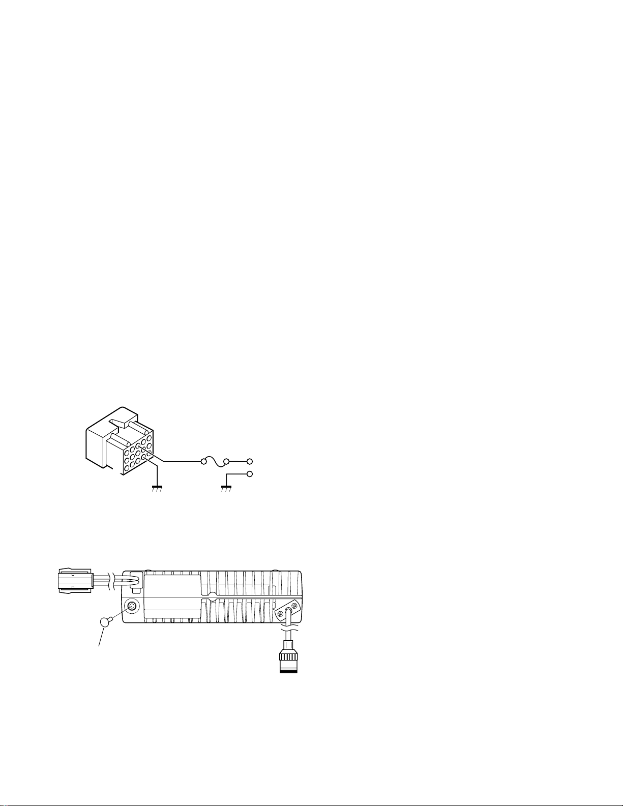
The rating of pin 7 (SB) of the accessory connector cable
(KCT-19) on the rear of the radio is 13.6V (1A). Insert a 1A
fuse if you use the SB pin for external equipment.
Accessory connector
cable (KCT-19)
1
7
13
15
3
6
+
–
1. Operation Features
The TK-980/981 is an 800MHz/900MHz band EFJ LTR™ compatible trunked radio designed to operate in both
trunking and conventional modes. The programmable features are summarized.
This model can handle up to 32 systems with up to 250
groups in each system. The transceiver can be used in both
trunked mode and conventional mode. Systems, groups,
and their functions are programmed.
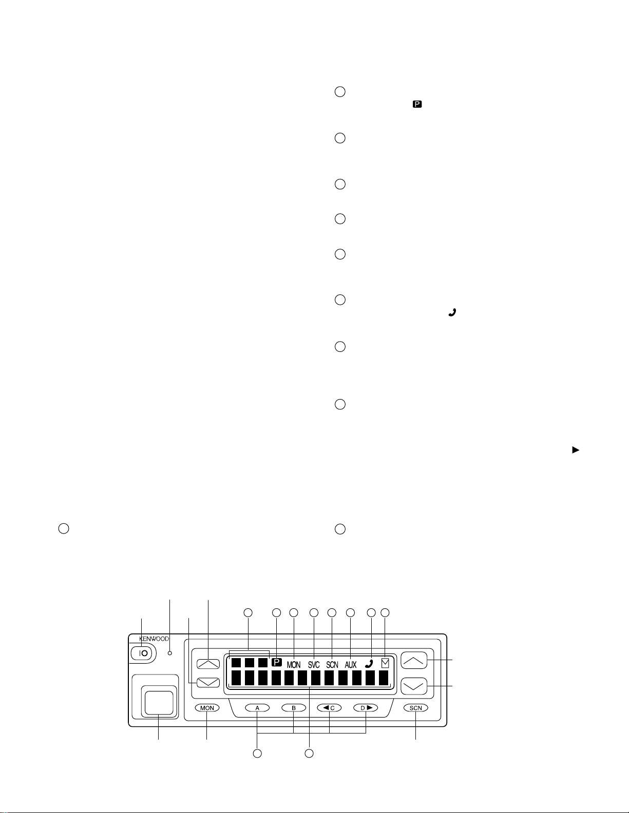
2. Transceiver Controls and Indicators (Fig. 1)
2-1. Front Panel Controls
All the keys on the front panel are momentary-type push
buttons. The functions of these keys are explained below.
• POWER key
Transceiver POWER key. When the power is switched
off, all the parameters, such as the system and group are
stored in memory. When the power is switched on again,
the transceiver returns to the previous conditions.
• SYSTEM UP/DOWN key (Programmable)
• SCAN key (Programmable)
• MONITOR key (Programmable)
• A, B, C and D key (Programmable)
• VOLUME UP/DOWN key (Programmable)
• BUSY/TX LED
The BUSY indicator (Green LED) shows that the group is
in use. The TX indicator (Red LED) shows that you are transmitting.
If you do not intend to use the 3.5-mm jack for the external speaker, fit the supplied speaker-jack cap (B09-0235-05)
to stop dust and sand getting in.
Speaker-jack cap
(B09-0235-05)
2-2. Programmable Keys
The FPU (KPG-49D) enables programmable keys to se-
lect the following functions.
Auto tel, AUX-A, AUX-B (Only when voice scrambler is
not selected), DTMF ID (BOT), DTMF ID (EOT), Display character, Emergency (Only foot key), Function, Group down,
Group up, Home group, Horn alert, Key lock, Memory (RCL/
STO), Memory (RCL), Memory (STO), Message mode (Only
A key), Monitor A, Monitor B, Monitor C, Monitor D, Public
address, Redial, Scan, Scan del/add, Scan temporary delete,
Scrambler (Only when voice scrambler is selected), Send
GPS, System down, System up, TEL disconnect, Volume
down, Volume up and None.
These functions the FPU programs to the function keys
and described in the following sections.
• Auto TEL
Automatically connects available repeaters that are connected to telephone circuits when operating as LTR system.
The time allocated to search for available repeaters is 60
seconds, after which connection failure occurs, a DTMF
tone is output and the function terminates.
If connection to an available circuit is made, only ID 253,
EOT or hang-up time-out can terminate the function.
3
Page 4

TK-980/98 1
OPERATING FEATURES
• AUX-A
If this key is pressed, “AUX” icon lights on the LCD and
AUX port which is inside of the transceiver turns to the high
level. If pressed again, the “AUX” icon goes off and the
AUX ports turns to the lower level.
• AUX-B
This function can be programmed when the voice scrambler board is not installed.
If this key is pressed, an underscore (“_”) appears at the
extreme right of the LCD and AUX port which is inside of the
transceiver turns to the active level. If pressed again, the
underscore disappears and the AUX ports turns to the
deactive level.
• DTMF ID (BOT)
In conventional mode, if you press this key, a predetermined DTMF ID (Begin of TX) will be sent automatically.
• DTMF ID (EOT)
In conventional mode, if you press this key, a predetermined DTMF ID (End of TX) will be automatically sent.
• Display character
This key switches the LCD display between the system
and group number and the system and group name.
• Horn Alert
If you are called from the base station using DTMF while
you are away from your transceiver, you will be alerted by
the vehicle horn or some other type of external alert. To turn
the horn alert function on , press this key. A confirmation
tone sounds, and the display shows “HA” on the sub LCD.
If this key is pressed again, the horn alert function is
turned off.
• Key Lock
Pressing this key causes the transceiver to accept entry
of only the [Function], [Key lock], [PTT], [Monitor A], [Monitor B], [Monitor C], [Monitor D], and [Emergency] keys.
• Message Mode
Press this key to enter the message mode. (See “Alphanumeric Two-way Paging Function” for details)
• Memory
This key allows DTMF memory data to be recalled; up to
32 memories each with a memory dial of up to 16 digits and
an A/N of up to 10 digits per memory.
• Monitor
Used to release signalling or squelch when operating as a
conventional. It is also used to reset option signalling.
• Emergency
Pressing this key for longer than the programmed “Emergency Key Delay Time” causes the transceiver to enter the
emergency mode. The transceiver jumps to the programmed “Emergency system and group” and transmits for
the programmed “Active Time”.
The transceiver disables mic mute while transmitting.
After finishing transmission, the transceiver receivers for
the programmed “Interval Time”. The transceiver mutes
the speaker while receiving. Following the above sequence,
the transceiver continues to transmit and receive.
• Function
Pressing this key causes the transceiver to display
“FCN”. Then, pressing a microphone DTMF key causes the
corresponding programmed function to start. This key may
be convenient when using many functions with the microphone 12-key keypad.
• Group Up/Down
When the key is pressed each time, the group number to
be selected is incremented/decremented and repeats if held
for one second or longer.
• Home Group
Each pressing of the key selects a preset system/group.
• Public Address
Public address amplifies the microphone audio, and outputs it through a PA speaker. PA is activated by pressing
this key. A confirmation tone sounds, and the display
shows “PUBLIC ADRS”. PA can be activated at anytime
(scanning or non-scanning).
The RADIO continues to scan & receive calls while in PA
mode. Pressing PTT activates PA, and will override an incoming call at anytime; however, no RADIO transmission
takes place.
If this key is pressed again, a confirmation tone will
sound, the display will return to the normal group or SCAN
display, and the PA function will turn off.
• Redial
If you press this key when the system/group is displayed,
the last transmitted DTMF code will appear on the display.
Pressing the PTT switch at this time will transmit the displayed DTMF code.
• Scan
Press this key starts scanning. Pressing this key stops
scanning.
• Scan Del/Add
Used to select whether system scan routines are used
during system scan. Each pressing of the key (to ON)
toggles between lockout and lock. The scan routine is
started when on lock. The DEL indicator flashes when the
system is on lockout.
4
Page 5
OPERATING FEATURES
TK-980/98 1
• Scan Temporary Delete
This key is temporarily deleted a system being scanned.
If you press this key when scan is stopped (when a call is
being received from another station), the system is temporarily deleted and scanning restarts.
This key operates even when “Scan Type” is set to “List
Type System Scan”.
• Scrambler
If a scrambler code (1 to 16) has been set in the FPU, an
underscore (“_”) appears at the extreme right of the LCD
display when scrambler is active. Pressing this key changes
on/off of scramble operation. Press this key for 2 seconds
to enter scrambler code selection mode.
• Send GPS (Optional)
Pressing this key causes the transceiver to send a single
GPS data. (GPS receiver must be installed.)
• System Up/Down
When the key is pressed each time, the system number
to be selected is incremented/decremented and repeats if
held for one second or longer.
• Telephone Disconnect
Pressing this key ends an RIC connection (disconnects
the telephone line).
• Volume Up/Down
When the key is pressed, the volume level is increased/
decreased and repeats if held for 200ms or longer.
• None
Sounds error operation beep, and no action will occur.
Use this function when the transceiver is required to be
more simple operated.
2-3. Front Panel Displays and Indicators
1
Sub display
Displays the system and group numbers. Also displays
various functions, such as TA.
2
P (Priority) indicator
The P indicator ( ) appears when a selected group is pro-
grammed as priority, in conventional operation.
3
MON (Monitor) indicator
The MON indicator appears when the button pro-
grammed as MONITOR is pressed.
4
SVC (Service) indictor
This icon is not used this transceiver.
5
SCN (Scan) indicator
The SCN indicator appears when using scan mode.
6
AUX (Auxiliary) indicator
appears when the auxiliary function is activated (ON) by
pressing the AUX-A key.
7
Handset indicator
The handset indicator ( ) appears when the selected
group is programmed as telephone IDs.
MAIL indicator
8
Flashes when a status message (FleetSync™) is received. Lights when a status message is stored in the stack
memory.
Alphanumeric display
9
The twelve-character dot matrix alphanumeric display
shows the system/group numbers. You can program system/group names with up to ten characters in place of these
numbers. The left display is used as a delete indicator (
and the right is used for the selective call (
(_) function. The delete indicator shows the systems
locked out of the scanning sequence. Selective call and
scrambler are optional functions that can be programmed.
Displays received messages when using FleetSync™.
10
A,B,C,D key
These keys are programmable function (PF) keys.
) or scrambler
*
)
POWER
MODULAR
MIC JACK
BUSY/
TX LED
VOLUME
DOWN
MONITOR
VOLUME
UP
2 3
1
10
4 5 6 7 8
9
SYSTEM UP
SYSTEM DOWN
SCAN
Fig. 1
5
Page 6

TK-980/98 1
OPERATING FEATURES
3. Scan Operating
■ System Scan
System scan can be selected with the “Scan” key by programming the scan feature. When the “Scan” key is
pressed and the “SCN” mark appears, scan mode in entered. Scanning starts from the system following the currently displayed system. When a call is received, scanning
stops, and the system and group are displayed.
When programming key is touched during scanning, the
scan stops and the revert system or group can be changed.
Scanning resumes one second after the key is released.
There are two types of system scan.
• Fix System Scan
All the set systems except locked-out ones are scanned.
If the Del/Add feature is assigned to the programmable key,
it can be controlled from the front panel.
• List Type System Scan
A scan list can be set for each system.
The list to be scanned can be changed by changing the
display system.
If many systems have been set, the scan speed can be
increased by narrowing the systems to be scanned with
scan lists.
■ System Lockout
The system lockout feature is used to lock systems out
of the scan sequence, and can be selected by programming
in the following two ways;
• Fixed Lockout
The system to be locked out is selected by programming.
When a locked system is selected, the Delete (
appears on the left of the SYSTEM indicator. The revert system is scanned even if it is locked out. If there is a locked
system, the Delete (
ning.
) indicator flashes during fixed scan-
• User Selectable Lockout
If the scan lockout feature is programmed to a key, the
user can lock systems out of the scan sequence with the
key. To lock a system out of the scan sequence, press the
key when the system is displayed. The Delete (
is displayed on the left of the SYSTEM indicator.
To unlock a system, select the system and press the key.
The Delete (
tem has returned to the scan sequence. The revert system
is scanned even if it is locked out. If there a locked system,
the Delete (
systems are locked out, the scan stops and only the revert
system is received.
) indicator disappears to indicate that the sys-
) indicator flashes during fixed scanning. If all
■ Drop-out Delay Time (Scan Resume Time)
If a call is received during scan, the scan stops. The scan
resume time can be programmed as 0 to 300 seconds in
one-second increments. The default value is 3 seconds.
) indicator
) indicator
■ Dwell Time
The dwell time is the time after transmission ends until
the scan resumes in scan mode. It can be set 0 to 300 seconds by programming. The default value is 3 seconds.
■ System/Group Revert
System/group revert can be programmed for one of the
following;
• Last Called Revert
The system or group changes to the revert system or
group when a call is received with the system or group being scanned.
• Last Used Revert
If a system/group call is received during scanning and the
PTT button is pressed for transmission and response within
the drop out delay time, the system or group is assigned as
the new revert system or group.
• Selected Revert
If the system/group was changed while scanning, the
newly selected system/group.
• Selected + Talkback Revert
If the system/group was changed while scanning, the
newly selected system/group. The transceiver “talks back”
on the current receive group.
■ Scan Massage Wait
The time for staying with the home repeater that receives a signal during system scan and monitoring data
messages can be programmed. If there is no signal from
the home repeater, the system is scanned for about 50ms.
If there is a signal, three data messages are monitored.
Normally, three data messages are monitored for each system, and it can be increased in multiples of three data messages per line to up to eight lines.
If the repeater data message indicates that there is no
call, data monitoring is terminated and the home repeater of
the next system is scanned.
■ Group Scan Operation
Group scan can be programmed for each group. In addition to the ID codes of the selected group, the ID codes of
the other groups that are permitted for group scan are decoded. (The two fixed ID and block decode codes are always decoded.)
If, during group scanning, a call is received with one of
the selectable group ID codes for which group scan is enabled, the group display indicates the group number that the
call came in with. That group then becomes the new selected group. Group scan resumes after the specified dropout delay time or dwell time shared by the system scan
elapses.
6
Page 7
OPERATING FEATURES
1s 0.5s 1s
TK-980/98 1
■ In Conventional System
If QT or DQT is set for the group, the groups, including
signalling, are scanned.
In case of the priority group is set in conventional system,
if a group scan (including group scan during a system scan)
temporarily stops (receiving) in a group that does not have
priority, a look back is performed to the priority group. Look
back is performed according to the look back time A and B
settings. If a call is received on the priority group, reception
immediately switches to the priority group.
4. Details of Features
■ Time-out Timer
The time-out timer can be programmed in 15 seconds
increments from 15 seconds to 10 minutes. If the transmitter is keyed continuously for longer than the programmed
time, the transmitter is disabled and a warning tone sounds
while the PTT button is held down. The alert tone stops
when the PTT button is released.
■ Sub LCD Display
You can use 3-digit the display to display the system
number or group number. It is useful when the main (12digit) display indicates system, group name or other functions.
■ Selective Call Alert LED
You can select whether or not the LED on the transceiver
flashes in an orange color when selective call was occurred.
■ Off Hook Decode
If the Off hook decode function has been enabled, removing and replacing the microphone on the hook has no
effect for decoding QT/DQT and option signalling.
■ Timed Power Off
This function works as “Automatic Power Switch Off”.
Timed power off timer starts from the ignition-off. After
the timer expires, the radio will automatically turn off. The
timer will be reset if the ignition is turned on and off.
This function requires ignition-sense. Connect the ignition-line to the 9-pin connector which is located at the rear of
the radio.
After the timer expires, press the power switch to turn
on the radio.
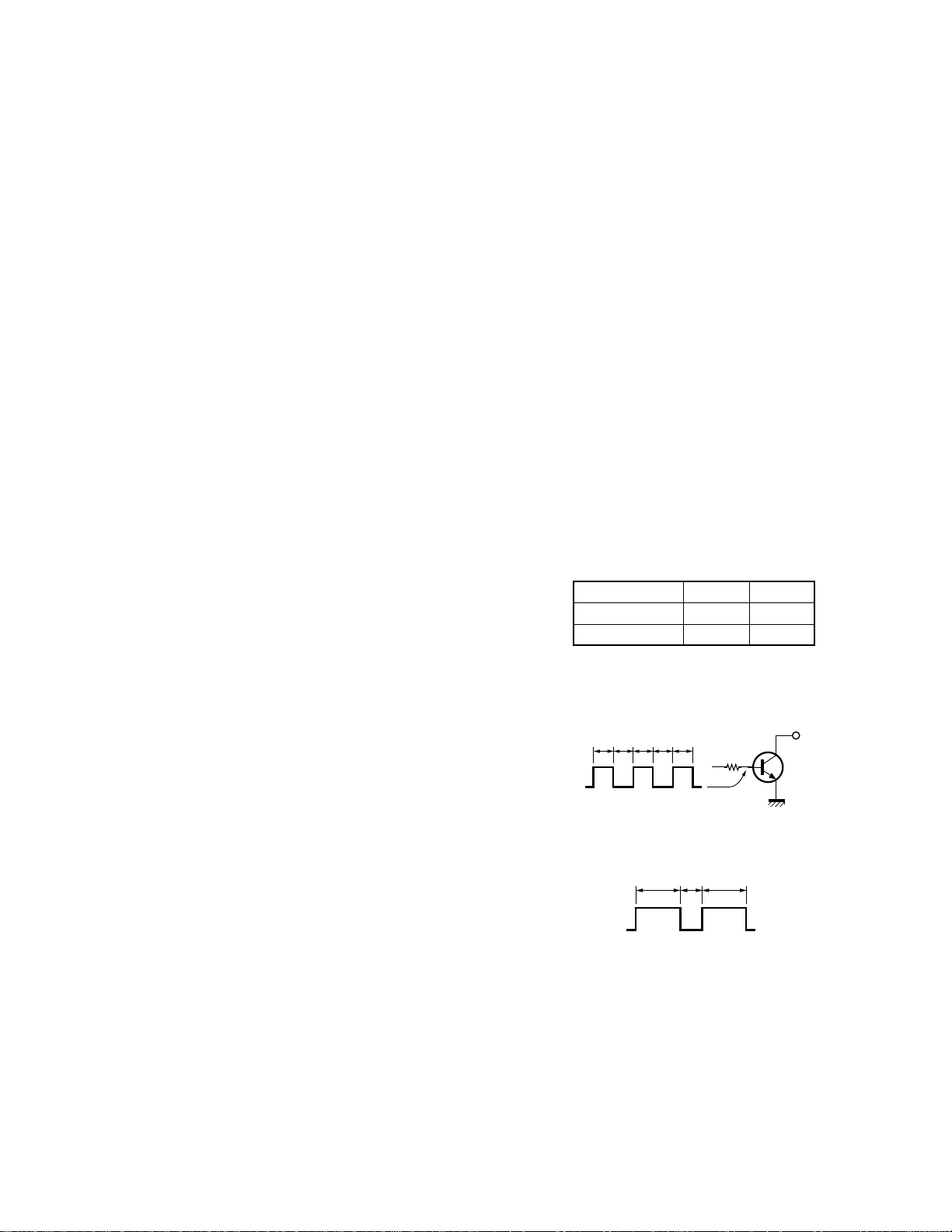
■ Horn Alert
Horn alert can be set to on or off for each group. If horn
alert has been set to YES for a group and DEC ID/QT/DQT/
MSK matches, the horn alert, HOR. is turned on and off.
The group for which the optional signalling is set works by
ANDing the decode ID/QT/DQT/MSK with the optional signalling.
Either continuous or non-continuous operation can be set
by the FPU. The horn alert port is enabled or disabled as
follows;
Off hook horn alert
Enable Yes Yes
Disable No Yes
Hook off Hook on
■ PTT ID
PTT ID provides a DTMF or MSK (FleetSync™ : Fleet-ID)
ANI to be sent with every time PTT (beginning of transmission, end of transmission, or both).
You can program PTT ID for each group. You can program PTT ID as “on” or “off” when “DTMF” is selected for
the PTT ID type. You can program a PTT ID as “own”, “sel”
or “off” when “MSK” is selected for the PTT ID type. The
contents of ID are programmed for each transceiver.
The timing that the transceiver sends ID is programmable.
BOT : DTMF ID (BOT)/MSK ID is sent on beginning of
transmission.
EOT : DTMF ID (EOT)/MSK ID is sent on end of transmis-
sion.
Both : DTMF ID (BOT)/MSK ID is sent on beginning of
transmission and DTMF ID (EOT)/MSK ID is sent on end
of transmission.
■ Radio Password
When the password is set in the transceiver, user can not
use the transceiver unless enter the correct password.
This code can be up to 6 digits from 0 to 9 and input with
the key, and “SCN” key.
■ Non-continuous
The horn alert port, HOR, is turned on and off as follows;
HOR
0.5s 0.5s 0.5s 0.5s 0.5s
The timing when the fixed LTR ID matches is as follows;
7
Page 8
TK-980/98 1
OPERATING FEATURES
■ Continuous
Horn alert can be reset by setting an expiration time from
the FPU, pressing the any key, or setting off hook.
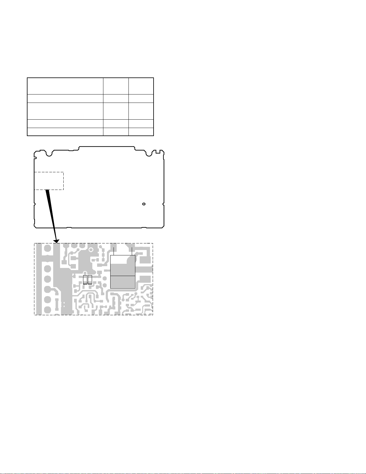
Operation when KCT-18 R151 R152
is connected
KCT-18 cannot be connected Enable Enable
Power on/off and Disable Enable
Horn alert on/off
Horn alert on/off Enable Disable
Power cannot be turned on Disable Disable
TX-RX unit A/2
Foil side
■ Free System Ringback
This feature is available only when a telephone interconnected ID code is selected. If a busy tone sounds when the
PTT button is pressed, the transceiver enters this mode automatically.
When the PTT button is released, a beep sounds for
400ms to indicate that the mode has been entered. If the
scan is on, it is resumed (the “SCN” mark goes on). When
any repeater becomes available, a ringing tone sounds and
this mode ends.
The mode is terminated when the system, group, scan,
PTT, key is changed.
■ System Search
This feature can be programmed to automatically access
other programmed systems when the selected system cannot be accessed. If an intercept tone sounds when the PTT
button is pressed after setting the mode, the transceiver
has entered the mode.
If the group ID is a telephone interconnect ID, the transceiver then attempts to access, in succession, other systems that have a telephone interconnect ID in the revert
group location. If the group ID is a dispatch ID, the transceiver attempts to access other systems that have a dispatch ID programmed in the revert group location.
If there is no system to be accessed, an intercept tone
sounds, the mode is terminated, and the transceiver returns
to the first system. If the access is successful, the mode is
terminated, and the searched system becomes the new selected system (If during scanning, the scan stops).
R151
R152
Q27
■ Call Indicator
The call indicator can be programmed for each group. In
trunked system, it can be set to respond to a selectable decode ID or one of two fixed IDs, except block IDs. When a
call is received with a selectable decode ID, the call indicator
flashes. When a call is received with a fixed ID, the call
indicator lights continuously.
On a conventional system, the call indicator can be programmed to light for each QT or DQT code. It keeps flashing while a call is being received. It is turned off by pressing
any front panel key.
■ Transpond
This feature can be programmed to turn on and off for
each group. If the ID of the group for which transpond is
enabled is received, two data messages (transmit ID and
turn-off code) are automatically transmitted if the PTT button is not pressed as a response within the time set (0 to
300 seconds in 1-second increments). If the PTT button is
pressed within the time, the transpond is not preformed.
■ Data TX with QT/DQT
Whether programmed QT/DQT is modulated or not with
a data transmission except for Selcall. A radio unit can receive a data message regardless of QT/DQT if the receiving
unit is not scanning.
■ Transmit Inhibit
The transceiver can be programmed with a transmit inhibit block of ID codes. If an ID code within this block is
decoded the preset time before the PTT button is pressed,
transmission is inhibited. The BUSY indicator lights and a
busy tone sounds until the PTT button is released to indicate
that transmission is not possible (except clear-to talk mode).
Transmission with the group for which the encode ID is
not set is inhibited, and the busy tone is output while the
PTT button is held down, regardless of the clear-to talk setting.
8
Page 9

OPERATING FEATURES
TK-980/98 1
■ Auto TEL
A telephone interconnect call can be made by simply
pressing the key by assigning this feature to the key. This
feature accesses the TEL channel of the available system
automatically.
When the key is pressed, a queue tone is output, and the
“AUTO TEL” appears on the alphanumeric display along
with a flashing handset indicator (
mode has been entered. If the TEL ID is set for the revert
system, the TEL channel of that system is accessed. If all
TEL channels are busy, an attempt is made to access the
TEL channels of another system in which the TEL ID code
has been programmed. It is repeated for 60 seconds until
the access succeeds. If the access succeeds, a dial tone
returns from the repeater. If the key is pressed again when
the queue tone is sounding, this mode is canceled.
If the access fails after 60 seconds, a deny tone is output
and this mode is terminated. When the talk ends, the revert
system/group returns. When the scan mode is effective,
the scan resumes. The Auto TEL feature can be programmed to turn on or off for each system.
) to indicate that this
■ ARQ Mode
If affects Trunking mode only. Automatic Repeat
reQuest (ARQ) mode is a manner to minimize the air traffic
of data communication. Also, it enables to occupy the
trunking repeater channel for the data communication period.
5. Option Signalling
5-1. DTMF
Built-in DTMF decoder is available for option signalling.
It is possible to use individual call, group call, D.B.D.
(Dead Beat Disable). D.B.D. is used with DTMF only.
If the option signalling matches, a predetermined action
will occur.
If option signalling matches on a group which is set up
with option signalling, the option signalling indicator (
flash and option signalling will be released. The transpond
or alert tone will sound.
If the selective call alert LED is set up, the orange LED
will flash.
While option signalling matches (or if option signalling is
deactivated when you are transmitting), you can mute or
unmute ID/QT/DQT/Carrier.
■ AND/OR
You can select AND or OR for option signalling match
conditions.
Alert/Transpond
AND QT/DQT/ID+DTMF; Option matches = Action
OR QT/DQT/ID+DTMF; Option matches = Action
AF mute open
AND QT/DQT/ID+DTMF; Option matches = Action
OR QT/DQT/ID; Signalling only matches = Action
*
) will
With OR set up, alert/transpond will not function with
only DTMF.
With OR set up, AF mute will not release when only
DTMF matches.
With a conventional group not set up with QT or DQT,
only the carrier is considered when signalling matches.
■ Auto Reset
If option signalling matches a group set up with option
signalling, option signalling is released. After matching option signalling, option signalling will temporarily reset automatically.
■ Dead Beat Disable
If the D.B.D. code matches, a predetermined action will
occur. Whether option signalling is activated or not, when
D.B.D. matches on any group, the transceiver will become
TX inhibited or TX/RX inhibited. While D.B.D. is active, if the
D.B.D. code + “#” code is received, D.B.D. will disactivate.
When D.B.D. matches, transpond will function. Alert will
not be output, and option signalling match icon will not appear.
5-2. MSK
Built-in MSK (FleetSync™ : Fleet-ID) decoder is available
for option signalling. When the group ID matches, squelch
remains muted while the station waits for reception of
proper MSK signal. When MSK signal matches, squelch
unmutes.
■ AND/OR
AND : QT/DQT/ID + MSK to unmute. MSK matches =
alert tone
OR : QT/DQT/ID to unmute. MSK matches = alert tone
6.
Alphanumeric Two-way Paging Function
(FleetSync™)
■ General
The Alphanumeric Two-way Paging Function
(FleetSync™) is a Kenwood proprietary protocol. It enables
a variety of paging functions.
■ ID Construction
A radio unit ID is defined by a combination of 3-digit Fleet
and 4-digit ID numbers. Each radio unit must be assigned its
own Fleet and ID numbers.
■ PTT ID
A pre-programmed unique ID (own) can be sent at the
beginning of transmission and/or the end of transmission to
identify which radio unit is on air.
When selecting (sel) for MSK ID, the radio calls he specific Fleet user the same as selective call.
9
Page 10

TK-980/98 1
OPERATING FEATURES
■ Selective Call (SELCALL)
This is a voice call to a particular individual or group of
stations.
• Example of Call Types;
[100][ALL ] : <Group Call>
All the units whose fleet number is “100” are called.
[100][1000] : <Individual Call>
The unit, whose the fleet number is “100” and ID number is “1000”, is called.
[ALL][ALL ] : <Broadcast Call>
All the units are called.
[ALL][1000] : <Supervisor Call>
All ID “1000” are called regardless of their fleet number.
• Unit ID Encode Block
Encode ID Block can be set to limit manual dial ID. The
radio unit will not accept an ID other than these IDs which
are entered from the keypad. If Inter-fleet Call is enabled,
block ID setting affects each fleet group.
■ Status Message
Using a 2-digit number, you can send and receive a Status message which may be decided in your talk group. Each
Status may be displayed with 16 alphanumeric characters if
programmed in the radio. A maximum of 9 received messages can be stored in the stack memory, and it can be reviewed after reception. If the message memory becomes
full, the oldest one will be erased. The stack memory will be
cleared by turning radio power off.
• Status 80~99 (Special)
Status numbers from 80 to 99 are reserved for special
purposes. Entering these statuses from the DTMF keypad
can be inhibited.
Please notice that the following status numbers are used
for special purposes;
80~87 : Reserved for future use.
88 : Terminates to emergency mode.
89 : Request for horn alert.
90 : Remote stun on. Disable the received radio unit’s
TX.
91 : Remote stun on. Disable the received radio unit’s
TX/RX.
92 : Cancel remote stun. Enable the received radio unit’s
TX/RX.
93 : Acknowledgement status sent when the radio unit is
in stun mode (TX disabled).
94 : Acknowledgement status sent when the radio unit is
in stun mode (TX/RX disabled).
95~97 : Reserved for future use.
98 : Man down emergency status (For portable).
99 : Emergency Status.
Note : Remote stun works with DTMF D.B.D. function also.
• Automatic Status Response
If you pre-select a status number and leave the radio in
the Status Mode, it can automatically respond with the selected status number upon request from the base station.
(The request function is initiated by serial control on the
base station (Optional).)
■ Short Messase (Optional)
A maximum of 48 characters can be sent (External equipment is required). Received Short Messages will be displayed in the same manner as a Status Message. A maximum of 4 received messages can be stored in the stack
memory. In the Stack Mode, 3-digit LCD indicates the received Short Message as “M01”~”M04".
■ Long Message (Optional)
A maximum of 1024 characters can be sent (External
equipment is required). Received Long Message will not be
displayed or stacked in the radio memory but is output
through the COM (Data) port.
■ Emergency Function
Emergency status 99 will be sent at the beginning of
each emergency transmission.
• Emergency Status response
Either “Horn” or “Alert” can be selected for the called
radio unit’s response to reception of status 99 which is used
as an emergency status.
■ Other Functions
• Manual Dial
Fleet, ID and Status numbers can be entered from DTMF
keypad. (DTMF microphopne is required.)
• FleetSync™ Baud Rate
MSK data baud rate setting. The same rate must be set
as a communication partner.
1200bps :
Data communication is made in 1200bps. The communi-
cation area is much wider than 2400bps. Recommended
for repeater operation.
2400bps :
Data communication is made in 2400bps. The communi-
cation area is narrower than 1200bps, but it will decrease
the data traffic. Data rate 2400bps may not work prop-
erly depending on the repeater’s characteristic.
• Message Mode Timer
Message Mode Timer is a delay timer returning from
message/stack mode to Normal mode.
• Status/Short/Long Message on Data Group
Status/Short/Long Message transmission is made
whether on the Data System/Group.
10
Page 11

OPERATING FEATURES
TK-980/98 1
• Status/Short/Unit ID Message Serial Output
(Option)
Whether a received Status/Short message or PTT ID is
output or not from serial port.
• Caller ID Display
PTT ID is displayed on LCD.
• Call Alert (Continuous)
The radio can provide the alert tone repeatedly until next
operation.
• PTT ID Sidetone
This function allows a single beep sound after the PTT ID
(MSK) for FleetSync™ signalling is encoded.
• Caller ID Stack
The radio stores the last 3 received caller IDs to volatile
memory.
■ GPS Report (Optional)
ANMEA-0183 GPS unit must be installed.
• GPS Report Mode
GPS data can be sent automatically or upon request.
Manually sending GPS data works regardless of this setting.
Auto : GPS data is sent both automatically and by request. GPS Auto TX Interval and GPS Time Mark must
be adjusted if required.
Poll : GPS data is sent upon request from dispatcher.
• GPS Report Interval
Interval time between automatic GPS data transmis-
sions.
• Received GPS Data Output
Any selected sentence can be output through the radio
serial port (COM0 or COM1).
1) MAP HEADER NMEA1 ($GPGGA), NMEA2 ($GPGLL),
NMEA3 ($GPRMC)
NMEA-0183 standard command. This should be set according to your PC application.
2) MAP HEADER KW1 ($PKLDS)
This is a Kenwood original sentence which consists of
“$GPGLL + Fleet + ID + Status”. This item should be set
according to your PC application.
3) MAP HEADER KW2 ($PKLID)
This is a Kenwood original sentence which consists of
“Fleet + ID”. This should be set according to your PC
application.
■ Parameters
• GTC Count
Number of Go To data Channel messages to be sent be-
fore transmitting a data message if it is being made on Data
System/ Group. If a radio unit receives a GTC message, it
will move to the Data System/Group of the current system.
Increase this item to make sure the called radio unit moves
to the Data System/Group.
• Random Access (Contention)
When a channel (or all the repeater channels for Trunking
mode) is busy, radio unit will not transmit (depending on its
Busy Channel Lockout setting in conventional mode). As
soon as a channel is cleared, some transmissions may
crash. Random access is used to avoid this by employing a
random transmission sequence.
• GPS Time Mark (Per Mobile)
The amount of time from the 0 (zero) minute of the standardized GPS UTC time to starting the first transmission of
GPS data. It must be set to a different value for each radio
unit to avoid a transmission crash.
• Send GPS
Pressing this key causes the transceiver to send a single
GPS data.
• GPS Report On Data Group
GPS data transmission is made on the Data System/
Group.
• Number of Retries
Number of Retries is the maximum number of retry
transmission when no acknowledgement is received in the
Maximum ACK Wait Time. Increase this item to improve
data communication reliability.
• TX Busy Wait Time
TX Busy Wait Time is the maximum amount of time before giving up the data transmission when the channel (or all
the repeater channels for Trunking mode) is busy. Also, this
timer affects if it expires during Random Access period.
• Maximum ACK Wait Time
Maximum ACK Wait Time is the maximum amount of
time to wait for an acknowledgement from the called radio
unit. It is used as an interval time of retries. It must be set
greater than the ACK Delay Time of the called radio unit.
11
Page 12

TK-980/98 1
OPERATING FEATURES
• ACK Delay Time
ACK Delay Time is the amount of time from the end of
receiving a data to the beginning of sending an
acknowledgement. It should be adjusted as the repeater’s
hang-up delay time. Also, it must be set less than the Maximum ACK Wait Time of the calling radio unit.
• TX Delay Time (RX Capture)
TX Delay Time is the amount of unmodulated transmission to let the called unit stop scanning or exit its battery
save mode. It is used only when starting a data communication sequence.
• Data TX Modulation Delay Time
Data TX Modulation Delay Time is the amount of time
from the beginning of transmission to the beginning of a
data modulation. It is used every time data is transmitted.
It must be set to more than 300ms if data communication is
made in Trunking Mode.
7. Audible User Feedback Tones
The transceiver outputs various combinations of tones to
notify the user of the transceiver operating state. The main
tones are listed below.
The high tone is 1477Hz, the mid tone is 941Hz, and the
low tone is 770Hz.
■ Power On Tone
This tone is output when the transceiver is turned on.
(The high tone is output for 500ms.)
■ Alert Tone
This tone is output when the transceiver is TX inhibition
for TOT and PLL unlocked. It is output until the PTT button
is released. (The 697Hz tone is output.)
■ DBD On Tone
When a D.B.D. code is received, transpond tone sounds.
■ DBD Off Tone
When a D.B.D. release code is received, transpond tone
sounds.
■ Password Agreement Tone
When the correct password is entered, the tone sounds.
The optional feature’s control tone can be set to yes or no.
■ PTT Release Tone
When you release the PTT switch, the PTT release tone
sounds.
■ Busy Tone
Sounds in LTR mode, when you cannot use a repeater
(system busy or TX inhibit). Sounds in conventional mode,
when busy channel lockout is functioning. You can select
yes or no for the optional feature’s warning tone.
■ Group Call Tone
Sounds when a group call with the correct DTMF option
signalling is received, repeats 7 times. You can select yes or
no for the optional feature’s warning tone.
■ Individual Call Tone
Sounds when an individual call with the correct DTMF
option signalling is received. You can select yes or no for
the optional feature’s warning tone.
■ Key Press Tone [A]
Sounds when a key is pressed. For toggle keys, sounds
when toggle function is turned on (key press tone [B]
sounds when it is turned off). You can select yes or no for
the optional feature’s control tone.
■ Key Press Tone [B]
Sounds when a key is pressed. For toggle keys, sounds
when the toggle function is turned off (key press tone [A]
sounds when it is turned on). You can select yes or no for
the optional feature’s control tone.
■ Key Press Tone [C]
Sounds when a key is pressed. Also sounds when storing data, adding a DTMF code to memory, and when changing test mode settings. You can select yes or no for the
optional feature’s control tone.
■ Key Input Error Tone
Sounds when a key is pressed but that key cannot be
used. You can select yes or no for the optional feature’s
warning tone.
■ Roll Over Tone
Sounds at the smallest system/group. You can select
yes or no for the optional feature’s control tone.
■ Transpond Tone
Sounds when an individual call with the correct LTR/
DTMF option signalling is received. For group calls, only the
group tone will sound, not the transpond tone.
■ Intercept Tone
This tone indicates that the transceiver is out of range. It
indicates that the PTT button is pressed, and transmission
has started, but the repeater cannot be connected and talking is not possible. It is output until the PTT button is released. (The mid tone and low tone are output alternately in
200ms intervals.)
■ Delay Tone
This tone is output when the PTT button is pressed and
the repeater is accessed three times or more to indicate
connection with the repeater is delayed. This tone is the
same as the busy tone. (It is not output of clear to talk has
been set to yes.)
12
Page 13
TK-980/98 1
User mode
Panel test mode
PC mode
Firmware programming mode
Panel tuning mode
Data programming mode
PC test mode
PC tuning mode
Clone mode
OPERATING FEATURES / REALIGNMENT
■ Proceed Tone
This tone is output when the PTT button is pressed,
transmission starts, and the repeater is connected to indicate that the user can talk if the clear to talk function has
been set. (The high tone is output for 100ms.)
■ Queue Tone
This tone is output until the auto TEL function is set and
the TEL channel is accepted successfully. (The mid tone on
for 50ms, off for 50ms, and on for 50ms in 1 second intervals.)
■ Deny Tone
This tone is output if the auto TEL function is set, the
queue tone is output, but the TEL channel cannot be accessed within 60 seconds. It is similar to the intercept tone.
(The mid tone and low tone are output alternately in 150ms
intervals.)
■ Free System Ringback Mode Tone, System
Search Mode Tone
This tone indicates that the transceiver is free system
ringback mode or system search mode. (The mid tone is
output for 400ms.)
■ Ringing Tone
This tone indicates that the transceiver can use the repeater in free system ringback mode. (The mid tone and no
tone are output eight cycles alternately in 50ms intervals.)
■ System Search Tone
Sounds when the system changes during system search.
You can select yes or no for the optional feature’s warning
tone.
REALIGNMENT
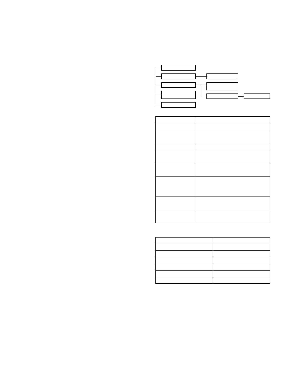
1. Modes
Mode Function
User mode For normal use.
Panel test mode Used by the dealer to check the funda-
ment characteristics.
Panel tuning mode Used by the dealer to tune the radio.
PC mode Used for communication between the
radio and PC (IBM compatible).
Data programming Used to read and write frequency data
mode and other features to and from the radio.
PC test mode Used to check the radio using the PC.
This feature is included in the FPU.
See panel tuning.
Firmware program- Used when changing the main program
ming mode of the flash memory.
Clone mode Used to transfer programming data from
one radio to another.
■ System Search End Tone
Sounds when a possible connection to a repeater in system search is not mode. You can select yes or no for the
optional feature’s warning tone.
2. How to Enter Each Mode
Mode Operation
User mode Power ON
Panel test mode [A]+Power ON (Two seconds)
PC mode Received commands from PC
Panel tuning mode [Panel test mode]+[SCN]
Firmware programming mode
Clone mode [C]+Power ON (Two seconds)
[SCN]+Power ON (Two seconds)
3. Panel Test Mode
Setting method refer to ADJUSTMENT.
4. Panel Tuning Mode
Setting method refer to ADJUSTMENT.
13
Page 14
TK-980/98 1
REALIGNMENT
5. PC Mode
5-1. Preface
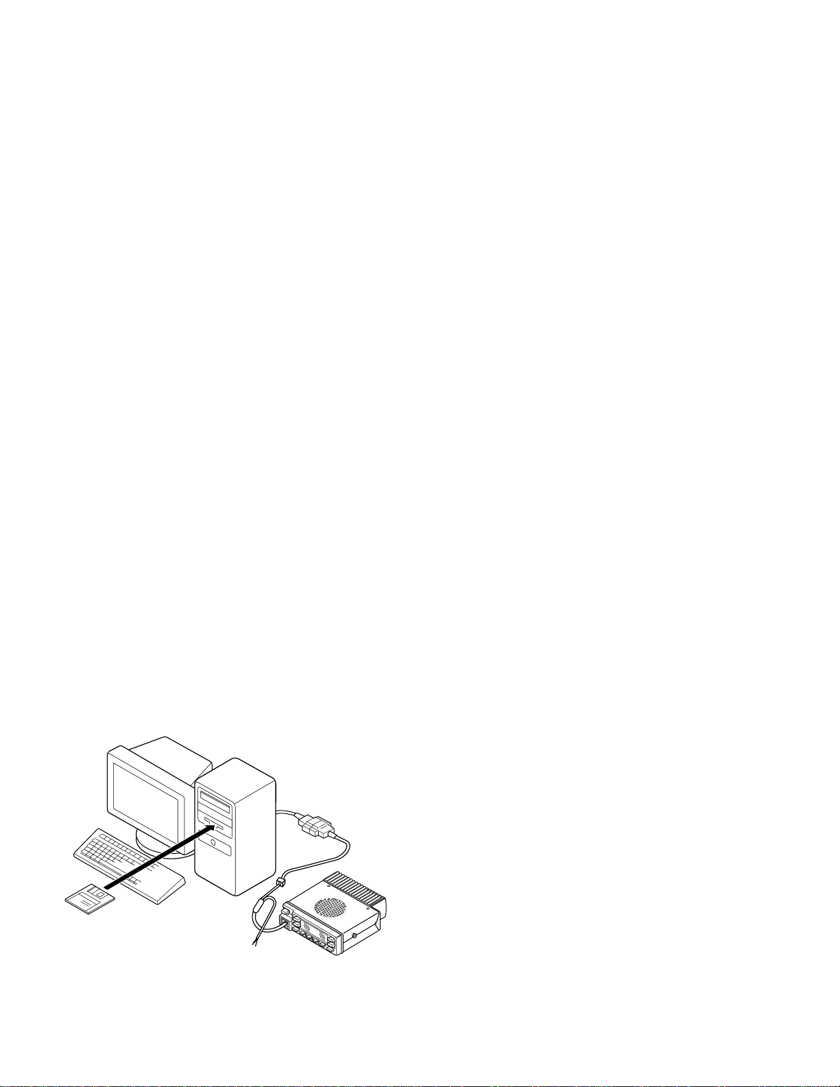
The transceiver is programmed by using a personal com-
puter, programming interface (KPG-46) and programming
software (KPG-49D).
The programming software can be used with an IBM PC
or compatible. Figure 1 shows the setup of an IBM PC for
programming.
5-2. Connection Procedure
1. Connect the transceiver to the personal computer with
the interface cable.
2. When the Power switch on, user mode can be entered
immediately. When PC sends command the radio enter
PC mode, and “PROGRAM” is displayed on the LCD.
When data transmitting from transceiver, the red LED is
blinking.
When data receiving to transceiver, the green LED is
blinking.
Notes :
• The data stored in the personal computer must match
model type, when it is written into the flash memory.
• Change the transceiver to PC mode, then attach the interface cable.
5-3. KPG-46 Description
(PC programming interface cable : Option)
The KPG-46 is required to interface the transceiver to the
computer. It has a circuit in its D-subconnector (25-pin) case
that converts the RS-232C logic level to the TTL level.
The KPG-46 connects the modular microphone jack of
the Ttransceiver to the computers RS-232C serial port.
5-4. Programming Software Description
The KPG-49D programming disk is supplied in 3-1/2" disk
format. The software on this disk allows a user to program
the transceiver radio via programming interface cable (KPG-
46).
IBM-PC
KPG-46
5-5. Programming With IBM PC
If data is transferred to the transceiver from an IBM PC
with the KPG-49D, the destination data (basic radio information) for each set can be modified. Normally, it is not necessary to modify the destination data because their values are
determined automatically when the frequency range (frequency type) is set.
The values should be modified only if necessary.
Data can be programmed into the flash memory in RS232C format via the modular microphone jack.
KPG-49D instruction manual parts No. : B62-1096-XX.
6. Firmware Programming Mode
6-1. Preface
Flash memory is mounted on the transceiver. This allows the transceiver to be upgraded when new features are
released in the future. (For details on how to obtain the
firmware, contact Customer Service.)
6-2. Connection Procedure
Connect the transceiver to the personal computer (IBM
PC or compatible) with the interface cable (KPG-46). (Connection is the same as in the PC Mode.)
6-3. Programming
1. Start up the programming software (KPG-49D), select
“firmware program” in the “Program” item, and press
the Return key on the personal computer. This starts up
the firmware programmer.
2. The top screen is displayed. Press any key to advance to
the next screen.
3. Set the communications speed (normally, 57600 bps)
and communications port in the Setup item.
4. Set the firmware to be updated by File select (=F1).
5. Turn the transceiver Power ON with the [SCN] switch
held down. Hold the switch down for two seconds until
the display changes to “PROG 57600”. When “PROG
57600” appears, release your finger from the switch.
6. Check the connection between the transceiver and the
personal computer, and make sure that the transceiver is
in the Program mode.
7. Press F10 on the personal computer. A window opens
on the display to indicate progress of writing. When the
transceiver starts to receive data, the [P] icon is blinking.
8. If writing ends successfully, the LED on the transceiver
lights and the checksum is displayed.
9. If you want to continue programming other transceivers,
repeat steps 5 to 8.
14
KPG-49D
Fig. 1
TK-980/981
Notes :
• To start the Firmware Programmer from KPG-49D, the
Fpro path must be set up by KPG-49D setup.
• This mode cannot be entered if the Firmware program-
ming mode is set to Disable in the Programming soft-
ware (KPG-49D).
• When programming the firmware, it is recommend to
copy the data from the floppy disk to your hard disk be-
fore update the radio firmware.
Directly copying from the floppy disk to the radio may not
work because the access speed is too slow.
Page 15
REALIGNMENT
TK-980/98 1
6-4. Function
1. If you press the [MON] switch while “PROG 57600” is
displayed, the checksum is displayed. If you press the
[MON] switch again while the checksum is displayed,
“PROG 57600” is redisplayed.
2. If you press the [D] switch while “PROG 57600” is displayed, the display changes to “PROG 19200” to indicate
that the write speed is low speed (19200 bps). If you
press the [D] switch again while “PROG 19200” is displayed, the display changes to “PROG 38400”, and the
write speed becomes the middle speed (38400 bps). If
you press the [D] switch again while “PROG 38400” is
displayed, the display returns to “PROG 57600”.
Note :
Normally, write in the high-speed mode.
7. Clone Mode
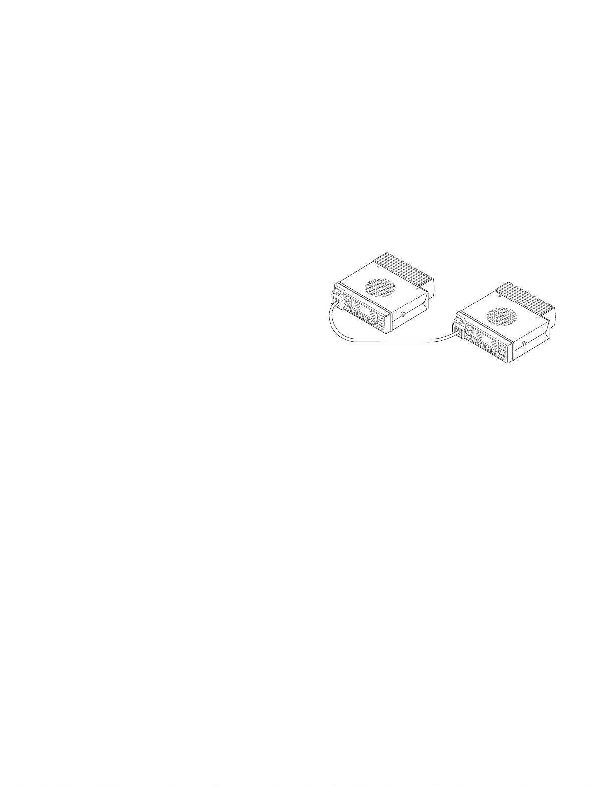
Programming data can be transferred from one radio to
another by connecting them via their modular microphone
jacks. The operation is as follows (the transmit radio is the
master and the receive radio is a slave).
1. Turn the master radio power ON with the [C] key held
down. If the password is set to the radio, the radio displays “CLONE LOCK”. If the password is not set, the
radio displays “CLONE MODE”.
2. When “CLONE LOCK” is displayed, only the [System up/
down] key and [SCN], and [0] to [9] keys can be accepted.
When you enter the correct password, and “CLONE
MODE” is displayed, the radio can be used as the cloning
master. The following describes how to enter the password.
3. How to enter the password with the microphone keypad.
If you press a key while “CLONE LOCK” is displayed, the
number that was pressed is displayed on the radio. Each
press of the key shifts the display in order to the left.
When you enter the password and press the [SCN] key,
“CLONE MODE” is displayed if the entered password is
correct. If the password is incorrect, “CLONE LOCK” is
redisplayed.
How to enter the password with the [System up/down]
key;
If the [System up/down] key is pressed while “CLONE
LOCK” is displayed, numbers (0 to 9) are displayed flashing. When you press the [SCN] key, the currently selected number is determined, and the display shifts to
the left. If you press the [SCN] key after entering the
password in this procedure, “CLONE MODE” is displayed if the entered password is correct. If the password is incorrect, “CLONE LOCK” is redisplayed.
4. Power on the slave radio.
5. Connect the cloning cable (No. E30-3382-05) to the
modular microphone jacks on the master and slave.
6. Press the [SCN] key on the master while the master displays “CLONE MODE”. The data of the master is sent to
the slave. While the slave is receiving the data, “PROGRAM” is displayed. When cloning of data is completed,
the mater displays “END”, and the slave automatically
operates in the User mode. The slave can then be operated by the same program as the master.
7. The other slave can be continuously cloned. When the
[SCN] key on the master is pressed while the master displays “END”, the master displays “CLONE MODE”.
Carry out the operation in step 4 to 6.
Note :
Only the same models can be cloned together.
Cloning cable
(E30-3382-05)
Fig. 2
15
Page 16
TK-980/98 1
INSTALLATION
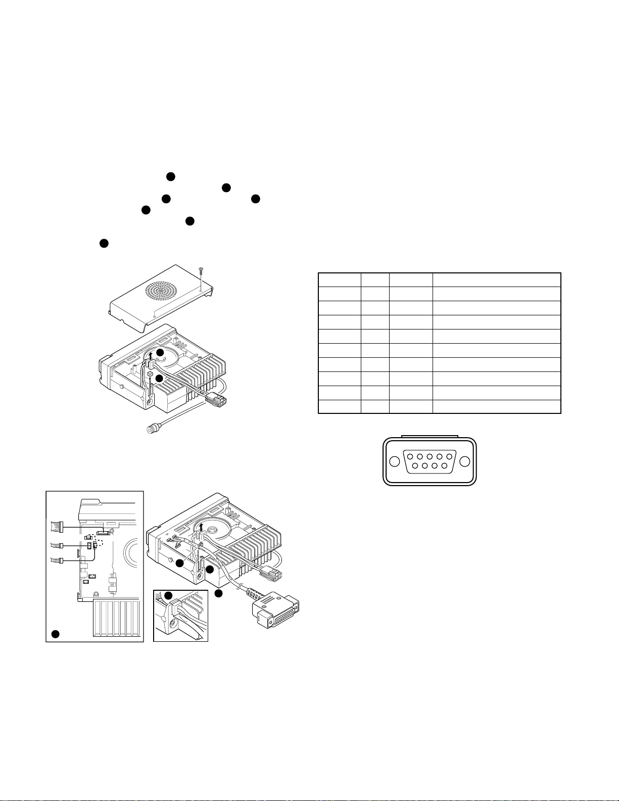
1. Accessory Connection Cable (KCT-19 : Option)
The KCT-19 is an accessory connection cable for con-
necting external equipment. The connector has 15 pins and
the necessary signal lines are selected for use.
1-1. Installing the KCT-19 in the transceiver
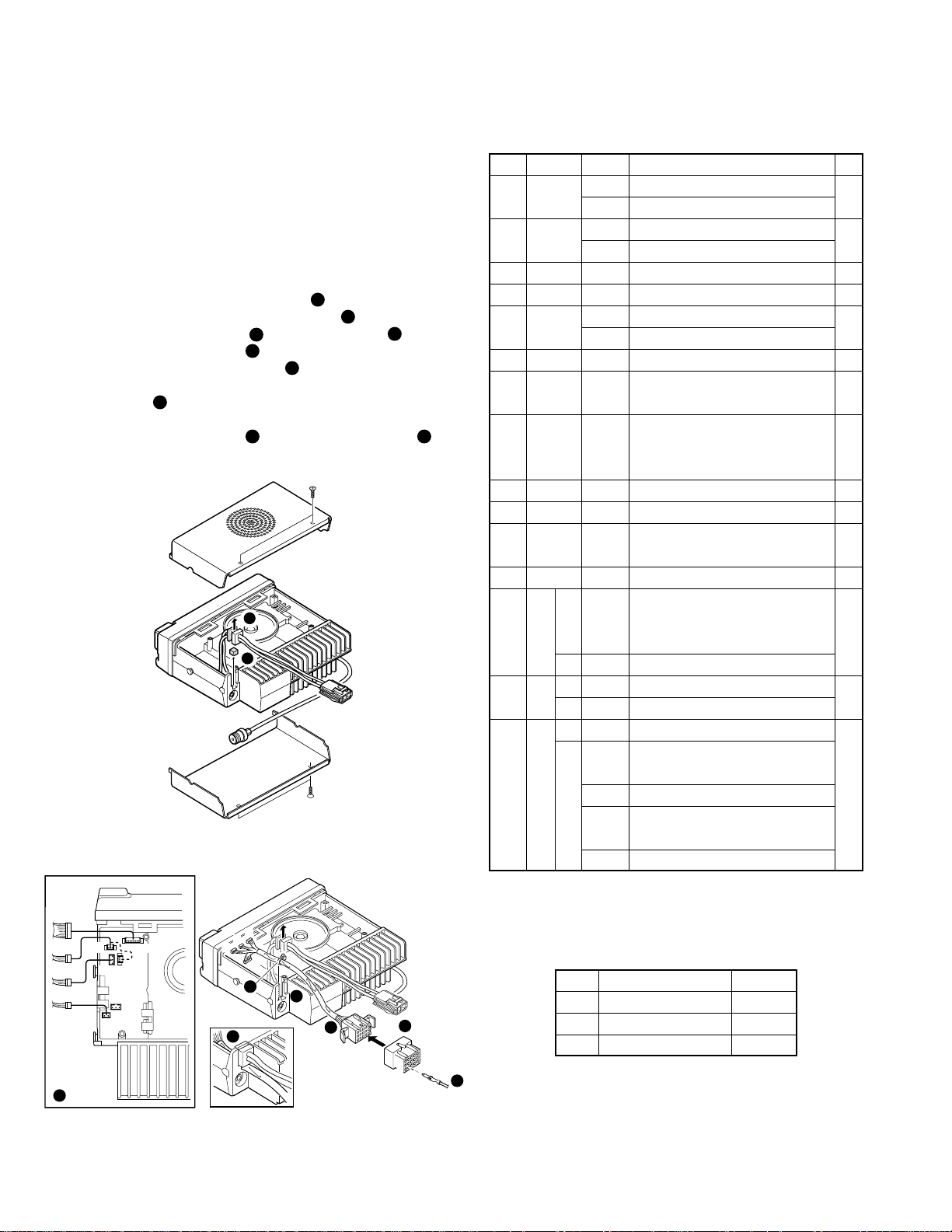
1. Remove the upper and lower halves of the transceiver
case, and lift the DC cord bushing (
2. Remove the pad as shown in Figure 1 (
3. Insert the KCT-19 cable (
The wire harness band (
) into the chassis ( 4 ).
3
) must be inside the chassis.
5
4. Replace the DC cord bushing (
5. Connect the KCT-19 to the TX-RX unit (A/2) as shown in
Figure 2 (
).
7
6. Connect the KCT-19 to the external accessory by inserting the crimp terminal (
) into the square plug ( 9 ),
8
both of which are supplied with the KCT-19.
1
2
Fig. 1
) from the chassis.
1
).
2
).
6
1-2. Accessory Port Function
No. (A)
No. (B,C,D,E)
1 D-2 AHK External hook input *1
2 D-5 ME Microphone ground *1
3 D-3 IGN Ignition sense input
4 D-1 DEO Receiver detector output
5 D-6 MI External microphone input *1
6 B-2 E Ground
7 B-3 SB Switched B+, DC 13.6V output.
8 D-7 PTT External PTT input, active low.
9 D-4 DI Data modulation input
10 B-1 HOR Horn alert/call output
11 D-8 SQ
12 C-1 SP Speaker audio output.
13 E-1
14 E-2
15 E-3
Name Function
BUSY System busy output
AM Speaker audio mute input
TXS Transmitter sense output
Maximum 1A
During DTC is low, it works as
DATA PTT.
Squelch detect output (Conventional)/
Logic squelch output (LTR), active low.
CN2
LOK Link complete pulse output. *2
and
CN4
CN2
AM Speaker mute input.
CN4
RXD Serial control data input *2
CN2
MM MIC mute input, active high.
CN4
TXD Serial control data output. *2
CN2
DTC Data control channel signal input,
Data channel : Low
LOK Link complete pulse output.
TXS Transmitter sense output,
Active high
FSW Foot switch input, active low
Note
16
Note
D
CN4
E
B
C
7
CN3
CN1
CN2
CN6
E
C
B
B
D
5
4
9
6
3
Crimp terminal
(E23-0613-05)
A
13
15
Square plug
(E09-1571-05)
1
3
Contact
12
*1 : The functions of A-1, A-2 and A-5 are changed as described in
the jumper chart.
*2 : The functions of A-13, A-14 and A-15 are changed if the con-
nector E is connected to CN2 or CN4 of the radio.
No. CN2 CN4
E-1 LOK/AM LOK
E-2 MM RXD
E-3 LOK/DTC/TXS/FSW TXD
· Connect CN6 of the radio to connector C of the KCT-19 instead of
8
to the internal speaker connector, if use external speaker.
Fig. 2
Page 17
INSTALLATION
TK-980/98 1
1-3. Data Equipment Connection
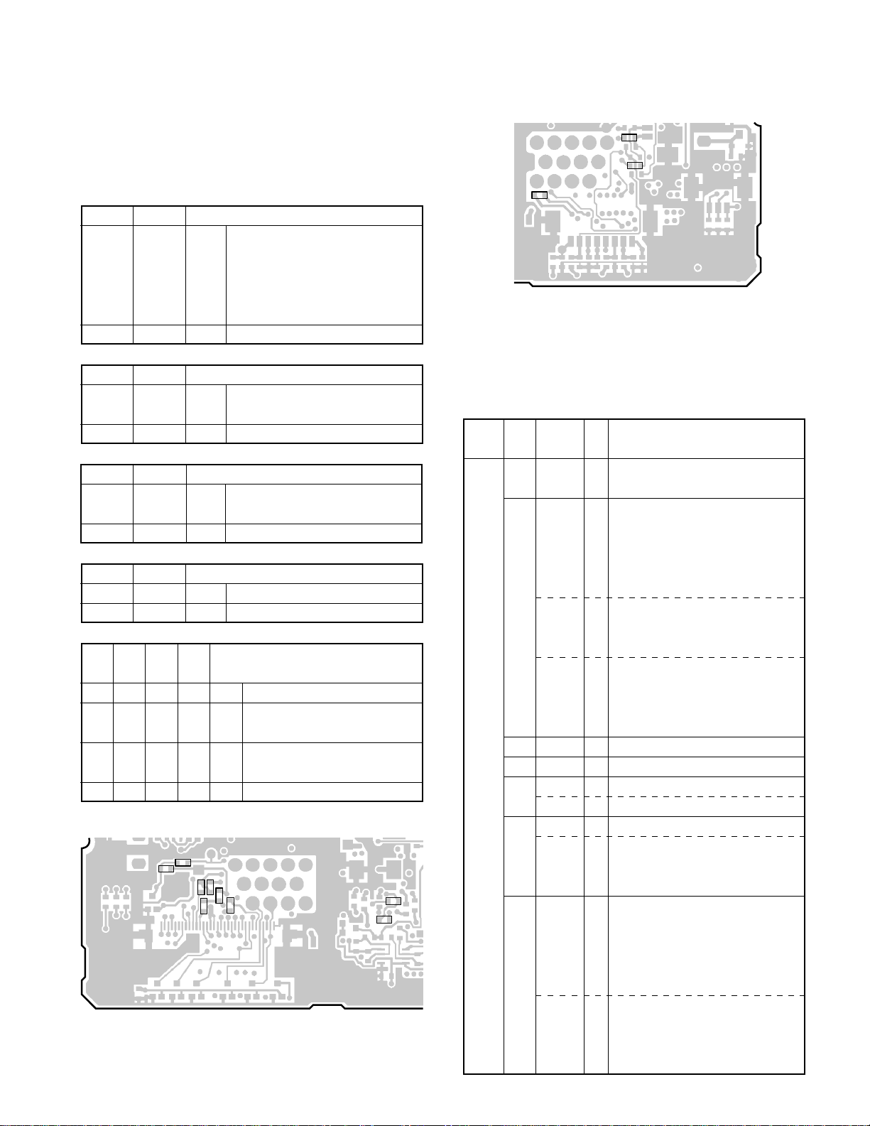
The jumpers must be set to either one for each function.
Otherwise, the radio will not work properly.
AHK/BUSY
R64 (0Ω) R18 (0Ω) Function
Yes No BUSY System busy output indicates if no
repeater channel is available in the
currently selected LTR system
when PTT is pressed, active low
: Default
No Yes AHK MIC hook input/RXD2 (com2).
ME/AM
R12 (0Ω)
MI/TXS
R94 (0Ω) R24 (0Ω) Function
LOK/AM
R5 (0Ω) R6 (0Ω) Function
DTC/LOK/TXS/FSW
R168 R84 R51 R13 Function
(0Ω)(0Ω)(0Ω)(0Ω)
No No No Yes LOK Link complete pulse output.
Yes No No No DTC
No No Yes No TXS Transmitter sense output,
No Yes No No FSW Foot switch input, active low
R167 (0Ω)
Yes No AM Speaker mute input, active high
: Default
No Yes ME MIC ground.
Yes No TXS Transmitter sense output, active
high : Default
No Yes MI Internal MIC input.
Yes No AM Audio mute signal input.
No Yes LOK
R13
R51
Link complete pulse output : Default
R12
R167
R94
R24
Function
Data control channel signal input,
Data channel : low (Default)
active high
R168
R64
TX-RX unit (A/2)
Foil side view
R18
R6
R5
R84
TX-RX unit (A/2)
Component side view
Note : The following parts are not installed at the time of
shipping; R5,R13,R18,R24,R51,R84,R167
2. Accessory Terminal (TX-RX Unit)
2-1. External Connector Accessory Terminal Method
Connector
Pin Pin I/O Function
No. No. name
CN1 1 DEO O Detect signal output. (Output level :
(DO) 250mVrms; standard modulation)
2 AHK I external hook signal input.
(AH) “COM2” port must be select “AUX
HOOK/PTT” / “DATA PTT” function
in the KPG-49D.
On hook : L, Off hook : H
BUSY O System busy signal output for
trunking system. No vacant repeater
: L, Vacant repeater : H
RXD2 I Serial data input 2.
“COM2” port must be select
“REM” / “DATA” / “DATA+GPS”
function in the KPG-49D.
3 IGN (IG) I Ignition input for KCT-18.
4 DI I External modulation signal input.
5 ME – MIC earth.
AM I Audio mute signal input.
6 MI I Internal MIC input.
TXS O Signal indicating whether the
transceiver is transmitting or not.
TX : H, Another : L
7 PTT I External PTT signal input.
(PT) “COM2” port must be select
“AUX HOOK/PTT” / “DATA PTT”
function in the KPG-49D.
TX : L, Another : H
TXD2 O Serial data output 2.
“COM2” port must be select
“REM” / “DATA” / “DATA+GPS”
function in the KPG-49D.
17
Page 18
TK-980/98 1
INSTALLATION
Connector
Pin Pin I/O Function
No. No. name
8 SQ O Squelch signal output. Signal logic
type can select “Carrier operate
relay” or “Tone operate relay”.
Active logic level or type can select
in the KPG-49D.
CN2 1 AM I Audio mute signal input.
LOK O Access logic signal output.
Active level or type can be select-
able in the KPG-49D.
2 MM I MIC mute input.
3 DTC I Data control channel signal input.
Data channel : L, Normal channel : H
TXS O Signal indicating whether the trans-
ceiver is transmitting or not.
TX : H, Another : L
FSW I Foot switch signal input.
Foot sw on : L, Foot sw off : H
LOK O Access logic signal output.
Active level or type can be select-
able in the KPG-49D.
CN3 1 HOR O Horn alert signal output. Signal
output for horn relay drive (open
collector). L level during horn drive :
Max. sink current 100mA.
2 E – Earth.
3 SB O Power output after power switch
(DC 13.6V±15%, 0.75A max.).
CN4 1 LOK O Access logic signal output.
Active level or type can be select-
able in the KPG-49D.
2 RXD1 I Serial data input 1.
“COM1” port must be select “REM”
/ “DATA” / “GPS” / “DATA+GPS”
function in the KPG-49D.
3 TXD1 O Serial data output 1.
“COM1” port must be select “REM”
/ “DATA” / “GPS” / “DATA+GPS”
function in the KPG-49D.
CN5 1 PA O Relay for PA function in KAP-1
control signal. PA on : H, PA off : L
2 SPO O Audio signal input from KAP-1.
3 SPI I Audio signal output to KAP-1.
CN6 1 SP O Output for internal/external speaker.
2 E – Earth.
18
3. Optional Board Terminal
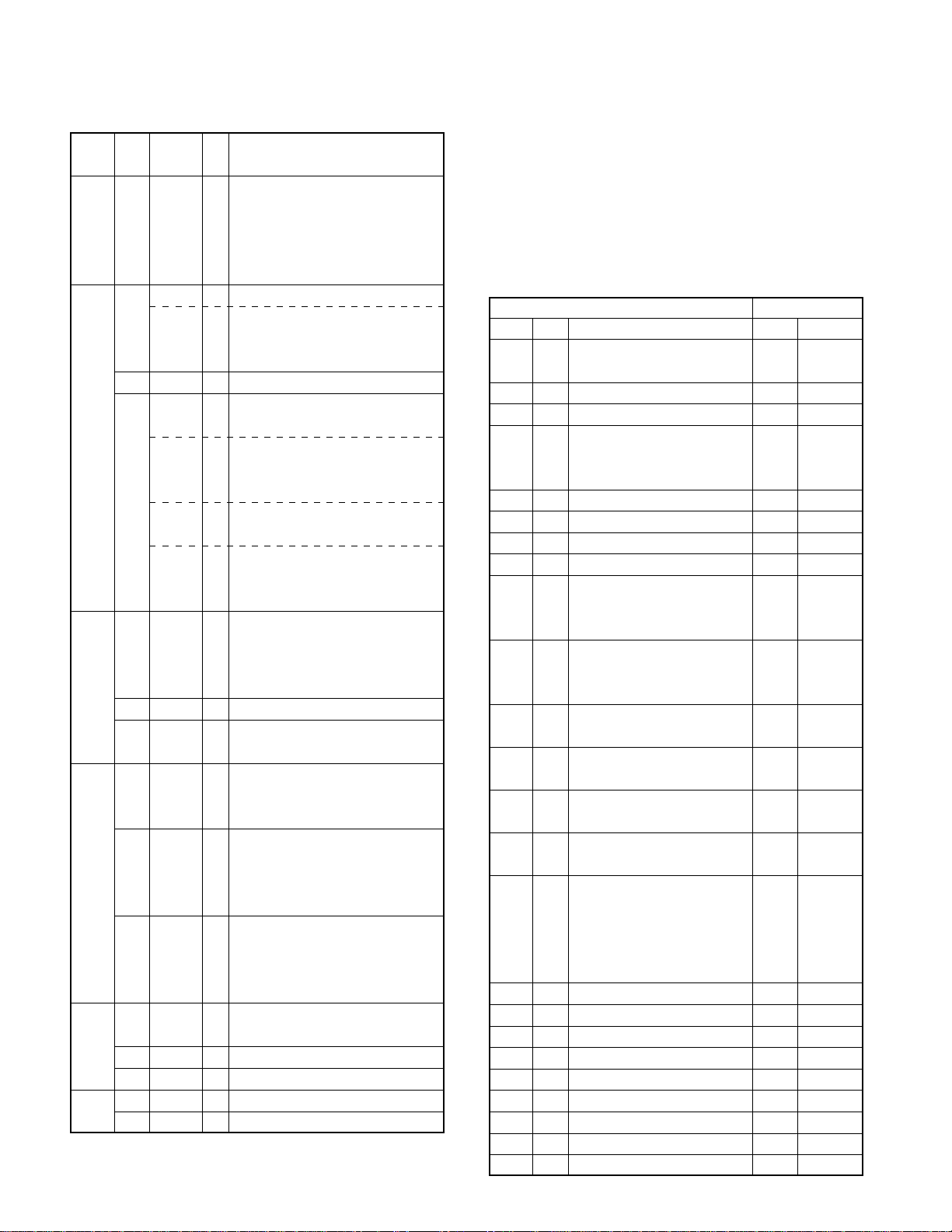
Terminal is for mounting the option board are provided at
the TX-RX unit (A/2) and TX-RX unit (B/2). The table below
shows the correspondence between the board and terminals. Disconnect R529 and R571 in control unit when the
scrambler board is attached.
The table below shown the differences between the
schematic terminals and the PC board terminals.
Schematic diagram PC board view
Name I/O Function Name Unit
SB – Switched B+, DC 13.6V SB
output. Maximum 0.75A
5C – 5C 5C
GND – Earth E
DEO O Detect signal output (Output DEO
level : 250mVrms; standard
modulation)
RXAI I RX audio input RXAI
RXAO O RX audio output RXAO
TXAI I TX audio input TXAI
TXAO O TX audio output TXAO
LOK O Access logic signal output. LOK
Active level or type can be
selectable in the KPG-49D.
OPT O Option board select. Please OP
(EMG) select option board type in the
KPG-49D.
OP1 O Option code 1 (for voice C1
scrambler code 1)
OP2 O Option code 1 (for voice C2
scrambler code 2)
OP3 O Option code 1 (for voice C3
scrambler code 3)
OP4 O Option code 1 (for voice C4
scrambler code 4)
SQ O Squelch signal output. Signal SQ
logic type can select “Carrier
operate relay” or “Tone operate
relay”. Active logic level or type
can select in the KPG-49D.
TXD1 O Serial data output 1 TD1
RXD1 I Serial data input 1 RD1
TXD2 O Serial data output 2 TD2
RXD2 I Serial data input 2 RD2
RSSI O
PTT I PTT PTT
MPTT I MIC PTT MPTT
FSW I Foot switch input FW
ST I Side-tone input ST
Receive signal strength indication
RSSI
TX-RX (A/2)
TX-RX (A/2)
TX-RX (A/2)
TX-RX (A/2)
TX-RX (B/2)
TX-RX (B/2)
TX-RX (B/2)
TX-RX (B/2)
TX-RX (A/2)
TX-RX (A/2)
TX-RX (A/2)
TX-RX (A/2)
TX-RX (A/2)
TX-RX (A/2)
TX-RX (A/2)
TX-RX (A/2)
TX-RX (A/2)
TX-RX (A/2)
TX-RX (A/2)
TX-RX (A/2)
TX-RX (B/2)
TX-RX (B/2)
TX-RX (A/2)
TX-RX (A/2)
Page 19
3
SB
R152
R151
KCT-19
ANT
CN7
TX-RX UNIT
(A/2)
1
2
3
KCT-19
Contact
KCT-18
13
15
1
3
6
LOK
E
DEO
TD2
RD2
RD1
TD1
5C
FW
INSTALLATION
C4
C3
SQ
OP
C2
C1
TK-980/98 1
RXAO
RXAI
TX-RX unit (A/2)
Foil side view
ST
TX-RX unit (A/2)
Component side view
R529
PTT
RSSI
Fig. 3
4-2. Modifying the Transceiver
Modify the transceiver as follows to turn the power or
the Horn Alert or Manual Relay function on and off with the
ignition key.
1. Remove the lower half of the transceiver case.
2. Set jumper resistors (0Ω) R151 and R152 of the TX-RX
unit (A/2) as shown in Table 1.
MPTT
TXAO
TXAI
R571
Foil side view
4. Ignition Sense Cable (KCT-18 : Option)
The KCT-18 is an optional cable for enabling the ignition
function. The ignition function lets you turn the power to the
transceiver on and off with the car ignition key.
If you use the Horn Alert function or the Manual Relay
function, you can turn the function off while driving with the
ignition key.
4-1. Connecting the KCT-18 to the Transceiver
1. Install the KCT-19 in the transceiver. (See the KCT-19
section.)
TX-RX unit (B/2)
2. Insert the KCT-18 lead terminal (
square plug (
the square plug into the KCT-19 connector (
) supplied with the KCT-19, then insert
1
) into pin 3 of the
2
).
Fig. 4
Operation when KCT-18 is connected. R151 R152
KCT-18 cannot be connected. Enable Enable
Power on/off and Horn Alert or Disable Enable
AUX-A on/off.
Horn Alert or AUX-A on/off, Enable Disable
Timed power off.
Power cannot be turned on. Disable Disable
Table 1 R151 and R152 setup chart
19
Page 20
TK-980/98 1
15
69
INSTALLATION
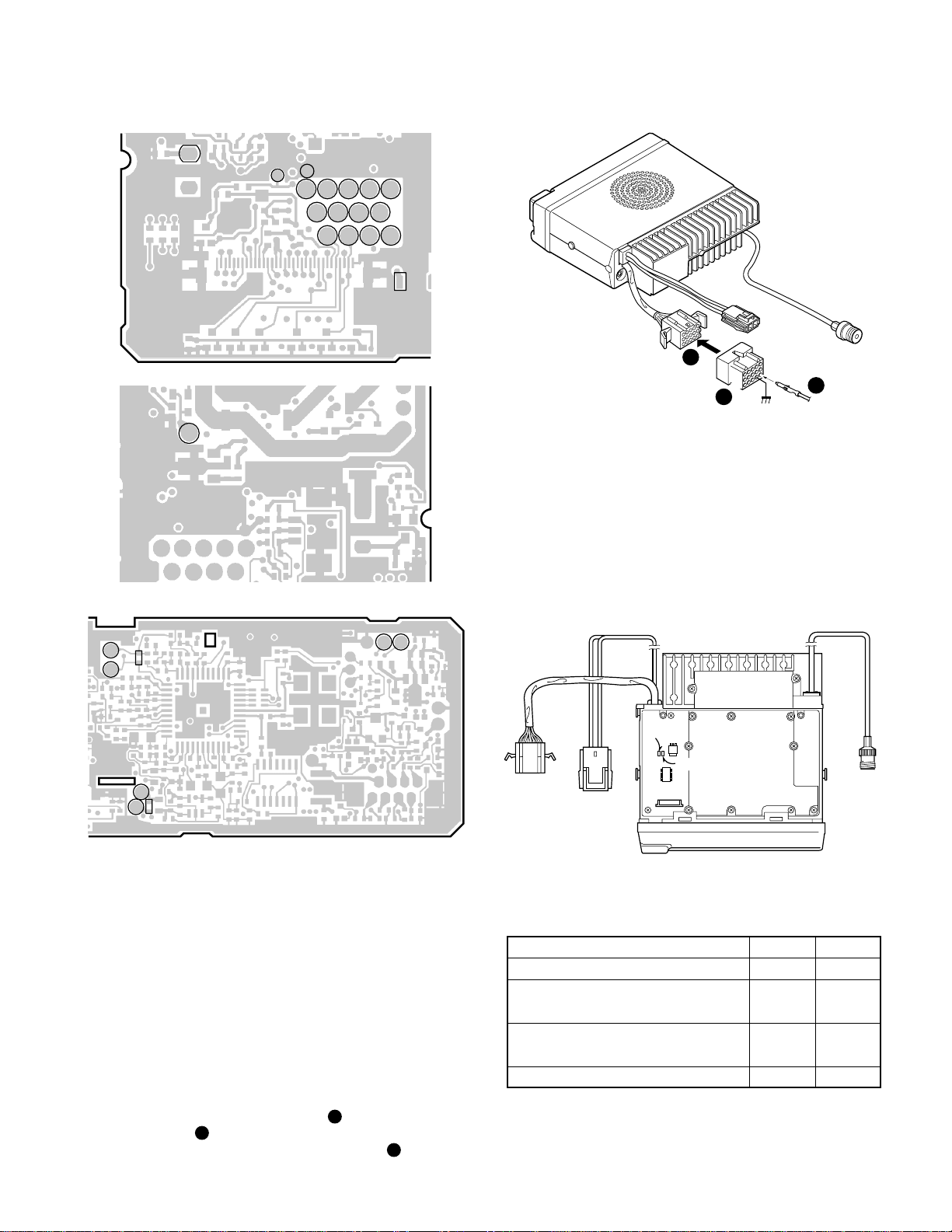
5. Connection Cable (KCT-29 : Option)
The KCT-29 connection cable kit is used to connect the
TK-980/981 transceiver to the KPG-1A Modem GPS Receiver or the KPG-1B Modem GPS Controller.
5-1. Installing the KCT-29 in the transceiver
1. Remove the upper cover from the transceiver.
2. Lift the DC cord bushing (
3. Remove the pad as shown in Figure 5 (
4. Insert the KCT-29 cable (
wire harness band (
5
5. Replace the DC cord bushing (
6. Connect the KCT-29 to the TX-RX unit (A/2) as shown in
Figure 6 (
).
7
) from the chassis.
1
).
2
) into the chassis ( 4 ). The
3
) must be inside the chassis.
).
6
1
2
6. Interface Cable (KCT-31 : Option)
The KCT-31 is a RS-232C interface cable for LMR mobile
radios, TK-980/981.
The 9-pin (D-sub) connector is connected to an external
RS-232C terminal. The other end of the cable is connected
to the internal connector of LMR mobile radio.
Note : You cannot write a firmware with the KCT-31.
6-1. Features
• This KCT-31 has a RS-232C-TTL level interface circuit.
• This KCT-31 does not require an external power supply.
• This KCT-31 can be used up to 9600 bps.
• Compatible with an ER terminal of DTE that has the volt-
age 6V or more.
6-2. Terminal function (D-sub connector)
Pin No. I/O Port name Function
1 I CD Carrier detect
2 I RD Receive data
3 O SD Transmit data
4 O ER Data terminal ready
5 – SG Signal ground
6 I DR Data set ready
7 O RS Request to send
8 I CS Clear to send
9 – CI Ring indicator
Fig. 5
C
CN4
D
B
7
CN3
CN1
CN2
B
B
D
C
5
4
6
3
KCT-29
A
Fig. 6
20
Page 21
INSTALLATION
TK-980/98 1
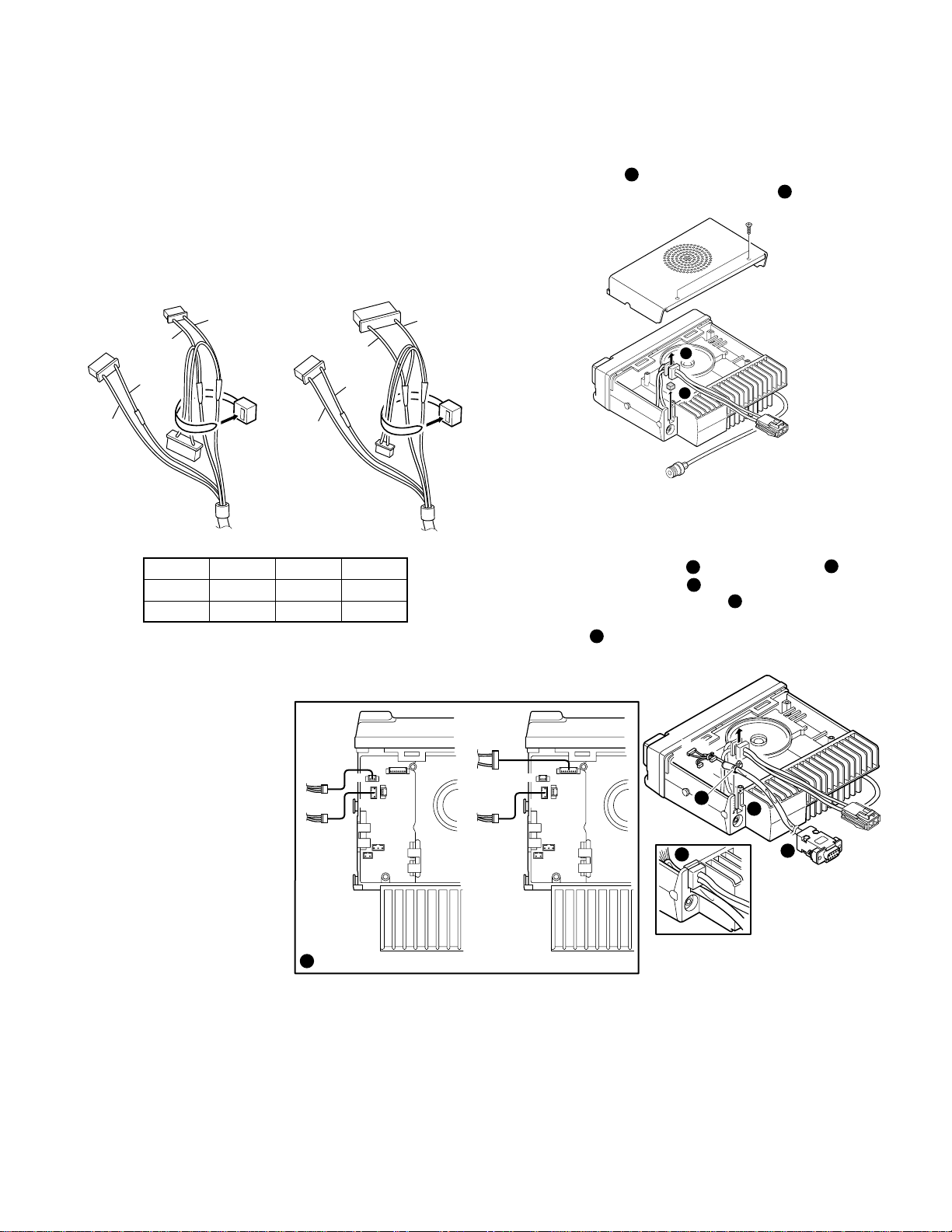
6-3. Installing the KCT-31 in the transceiver
Note :
When the COM1 is used, A connector is unused.
When the COM2 is used, C connector is unused.
1. Bind the unused connecor to the cable with a retaining
band as shown.
When the COM1 is used. When the COM2 is used.
B
Black
C
Yellow
Green
Red
A
ABC
COM1 No Yes Yes
COM2 Yes Yes No
B
Black
A
Yellow
Green
Red
C
Fig. 7
2. Make sure the unit’s power is turned off.
3. Remove the upper case of the transceiver and lift the DC
cable bushing (
4. Remove the pad as shown in Figure 8 (
) from the chassis.
1
1
2
).
2
Fig. 8
5. Insert the KCT-31 cable (
The write retaining band (
6. Replace the DC cable bushing (
7. Connect the KCT-31 to the TX-RX unit (A/2) as shown in
Figure 9 (
).
7
8. Replace the upper case.
) into the chassis ( 4 ).
3
) must be inside the chassis.
5
).
6
CN4
CN3
CN6
CN1
CN2
C
B
7
Note :
· The modification must be applied to the TK-980/981
transceivers with a serial number of 30600000 or smaller
when using a COM2 port. Replace the 47kΩ (R675) chip
resistor on the TX-RX unit (B/2) with a 4.7kΩ resistor.
Original New
47kΩ (RK73GB1J473J) → 4.7kΩ (RK73GB1J472J)
A
CN4
CN1
CN3
B
When the COM2 is used.When the COM1 is used.
CN2
CN6
A
B
5
6
4
3
Fig. 9
· Enable the serial port function on the terminal.
· Refer to the service manual of each radio or the help file
that came with the FPU (Field Programming Unit) for details.
21
Page 22
TK-980/98 1
HR1
HR2
TX-RX UNIT
(A/2)
KCT-19
CN7
PA
R109
ANT
INSTALLATION
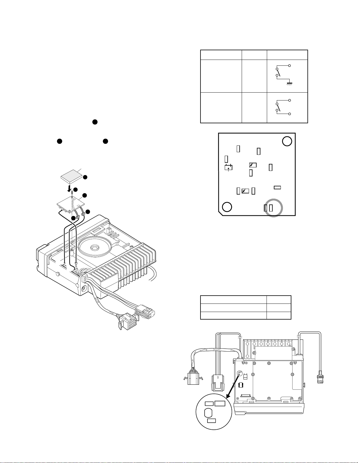
7. PA/HA Unit (KAP-1 : Option)
7-1. Installing the KAP-1 in the Transceiver
The Horn Alert (max. 2A drive) and Public Address functions are enabled by inserting the KAP-1 W1 (3P; white/
black/red) into CN3 on the TX-RX unit (A/2), inserting W2
(3P; green) into CN5 on the TX-RX unit (A/2), and connecting
the KCT-19 (option) to CN2 and CN3 of the KAP-1.
• Installation procedure
1. Open the upper case of the transceiver.
2. Insert the two cables (
KAP-1 switch unit into the connectors on the transceiver.
3. Secure the switch unit board to the chassis with a
screws (
). The notch ( 2 ) in the board must be
3
placed at the front left side.
4. Attach the cushion on the top of the KAP-1 switch unit.
3
W1
CN1
CN2
W2
CN3
1
) with connectors from the
1
Cushion
(G13-1710-04)
4
2
1
R1 Output form
HR1 (Default) Yes
HR2 No
Fig. 11 KAP-1 foil side view
HR1
R1
CN3
CN5
KCT-19
Fig. 10
7-2. Modifying the Transceiver
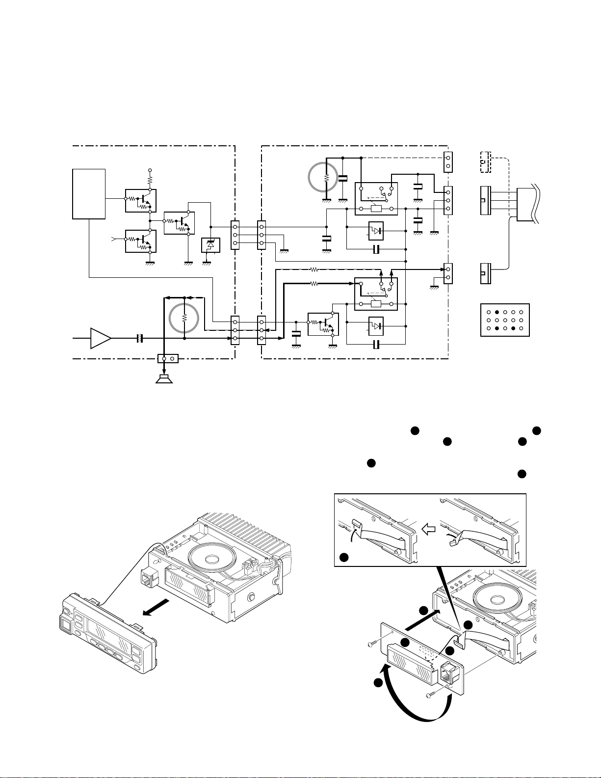
• Horn alert
The signal from pin 4 of IC7 on the TX-RX unit (A/2) turns
Q4 and Q6 on and off and drives KAP-1 HA relay to drive the
horn with a maximum of 2A.
The default output is HR1. The relay open output can be
obtained between HR1 and HR2 by removing R1 in the KAP-
1.
• Public address
The signal from pin 13 of IC7 on the TX-RX unit (A/2)
drives PA relay in the KAP-1 and switches the audio power
amplifier output between the external PA system (through
KCT-19) and internal and external speakers.
To use the PA function, R109 on the TX-RX unit (A/2)
must be removed.
R109
Use the PA function No
Do not use the PA function Yes
22
Fig. 12
Page 23
INSTALLATION
CN502
1
2
3
4
5
6
• Others
If the PA and HR2 are not necessary and the speaker output is output to an external unit through the KCT-19, connect
the KCT-19 C connector to CN6 on the TX-RX unit (A/2).
TK-980/98 1
TX-RX UNIT (A/2)
IC7
Shift
register
4
Q1
Q6
13
IGN
Audio
power amp
IC10
KAP-1 (SWITCH UNIT : X41-3380-20)
Q1 : DTD114EK
HOR
PA/LI
SPO
W1
E
SB
W2
SPI
D1,2 : 1SS193
1
2
3
1
2
C2
3
R3 0
R4 0
Q1
1000P
R1 0
C1
1000P
C5 1000P
±
C3 0.01
K1
±
C4 0.01
K2
C6
+
C7
D1
+
D2
8C
Q6
Q5
R58
Q4
R109
+
1
2
CN6
E
SP
Internal/External
speaker
CN3
D7
CN5
1000P
1000P
CN1
1
2
CN2
1
2
3
CN3
1
2
HR2
NC
HR1
E
SB
PAO/LIO
E
C
GRN
KCT-19
BRN
ORG
YEL
B
C
GRN
KCT-19 Terminal
13 10 1
12
15
6 : Earth
10 : HR1
12 : PA (HR2)
36
Fig. 13
8. Fitting the Control Panel Upside Down
The TK-980/981 control panel can be fitted upside down,
so the transceiver can be mounted with its internal speaker
(in the upper half of the case) facing down in your car.
2. Fold the flat cable ( 1 ) in the opposite direction ( 2 ).
3. Rotate the control section (
) 180 degrees ( 4 ).
3
4. Insert the flat cable into the control section connector,
CN502 (
5. Mount the control section on the transceiver (
).
5
6
).
6
1. Remove the control panel and the TX-RX unit (B/2) control section. (Fig. 14)
Fig. 14
Fig. 15
23
Page 24
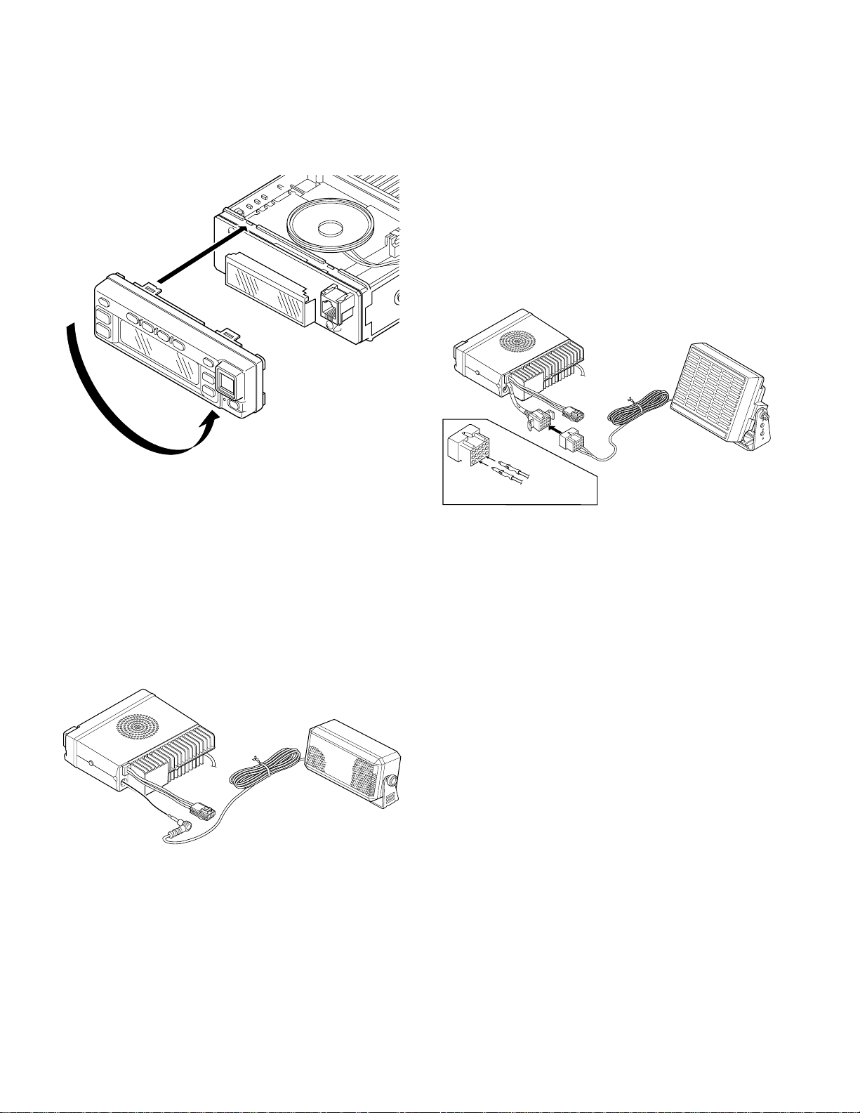
TK-980/98 1
INSTALLATION
6. Rotate the control panel 180 degrees and mount it on the
transceiver. Refit the two halves of the case to complete
installation. (Fig. 16)
Fig. 16
9. External Speaker
9-1. KES-3 : Option
The KES-3 is an external speaker for the 3.5-mm-diam-
eter speaker jack.
9-2. KES-4 : Option
The KES-4 is an external speaker used with the acces-
sory connection cable.
• Connection procedure
1. Install the KCT-19 in the transceiver. (See the KCT-19
section.)
2. Insert the crimp terminal into the square plug supplied
with the KCT-19.
3. Connect CN5 of the transceiver to connector C of the
KCT-19 instead of to the internal speaker connector.
KES-4
1
3
13
6
15
12
Crimp terminal
(E23-0613-05)
Black lead
Black/White lead
Fig. 18
• Connection procedure
1. Connect the KES-3 to the 3.5-mm-diameter speaker jack
on the rear of the transceiver.
KES-3
Fig. 17
24
Page 25
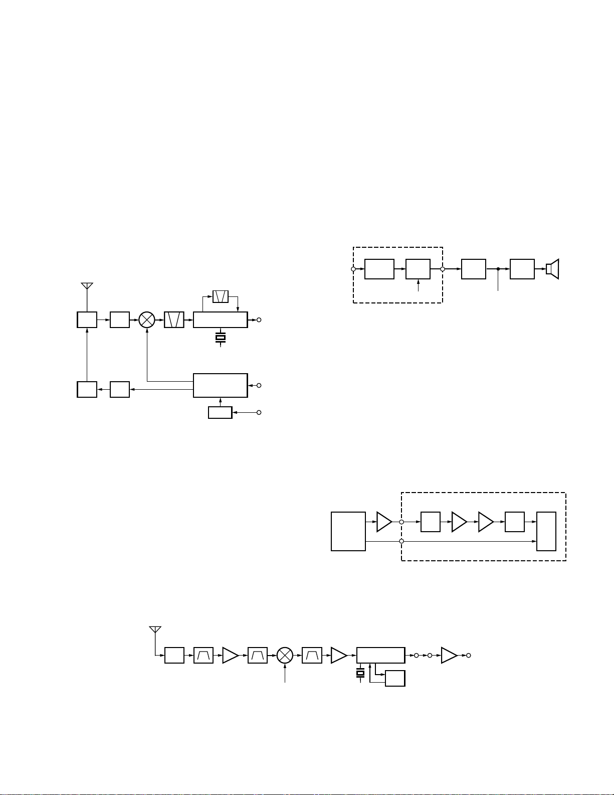
CIRCUIT DESCRIPTION
IC2
AMP
IC503
AMP
Q503
NOISE AMP
D509IC11 IC511
DEO
RSSI
HPF DET
CPU
IF
SYSTEM
TX-RX UNIT (B/2)
TK-980/98 1
Frequency Configuration
The TX-RX unit (A/2) incorporates a VCO, based on a fractional N type PLL synthesizer system, that allows a channel
step of 12.5kHz to be selected. The incoming signal from
the antenna is mixed with a first local oscillation frequency
to produce a first intermediate frequency of 44.85MHz.
The signal is then mixed with a second local oscillation
frequency of 44.395MHz to produce a second intermediate
frequency of 455kHz. This is called a double-conversion
system. The transmit signal frequency is generated by the
PLL VCO, and modulated by the signal from the microphone. It is then amplified by TX amplifier and PA amplifier,
and sent to the antenna.
TK-980
TX 806~825MHz
851~870MHz
RX 851~870MHz
ANT
ANT
SW
PA
AMP
Fig. 1 Frequency configuration
TK-981
TX 896~902MHz
RX 935~941MHz
RF
AMP
TK-980
806.15~
825.15MHz
TK-981
890.15~
896.15MHz
TX
AMP
935~941MHz
MCF
1st
44.85MHz
MIX
TK-980
806~825MHz
851~870MHz
TK-981
896~902MHz
935~941MHz
CF 455kHz
IF SYSTEM
44.395MHz
PLL/VCO
VCXO
16.8MHz
AFO
MD
MB
■ AF Signal System
The detection signal (DEO) from the TX-RX unit (A/2)
goes to the audio processor (IC504) of the TX-RX unit (B/2).
The signal passes through a filter in the audio processor to
adjust the gain, and is output to IC502. IC502 sums the AF
signal and the DTMF signal and returns the resulting signal
to the TX-RX unit (A/2). The signal (AFO) sent to the TX-RX
unit (A/2) is input to the D/A converter (IC5). The AFO output level is adjusted by the D/A converter. The signal output
from the D/A converter is added with the BEEP signal (BPO)
and the resulting signal is input to the audio power amplifier
(IC10). The AF signal from IC10 switches between the internal speaker and speaker jack (J1) output.
TX-RX UNIT (B/2)
IC10 SP
AF PA
DEO
IC504 IC504 IC5
AUDIO
PROCE.
SUM
AMP
DTMF BPO
AFO
CONV.
D/A
Fig. 3 AF signal system
■ Squelch Circuit
The detection output from the FM IF IC (IC11) is amplified by IC2 and the signal (DEO) is sent to the TX-RX unit (B/
2). The signal passes through a high-pass filter and a noise
amplifier (Q503) in the TX-RX unit (B/2) to detect noise. A
voltage is applied to the CPU (IC511). The CPU controls
squelch according to the voltage (ASQ) level. The signal
from the RSSI pin of IC11 is monitored. The electric field
strength of the receive signal can be known before the ASQ
voltage is input to the CPU, and the scan stop speed is improved.
Receiver System
■ Outline
An incoming RF signal from the antenna terminal passes
through the antenna switch (D208, D209, and D210 are off)
and then the bandpass filter (L203). The signal is amplified
by RF amplifier Q201, and passes through the bandpass filter (L207) again. The resulting signal goes to the first mixer
(Q203), where it is mixed with the first local oscillator signal
output from the frequency synthesizer to produce the first
IF 44.85MHz.
ANT
D208~210
ANT
SW
L203
BPF
RF AMP
Q201
L207
BPF
1st local
OSC (PLL)
Fig. 2 Receiver system
Q203
1st MIX
XF1
MCF
Q15
1st IF
MIX,DET,IF
X2
2nd
local OSC
Fig. 4 Squelch circuit
IC2
IC11
CF1
AF AMP
DET DET
DEO
25
Page 26
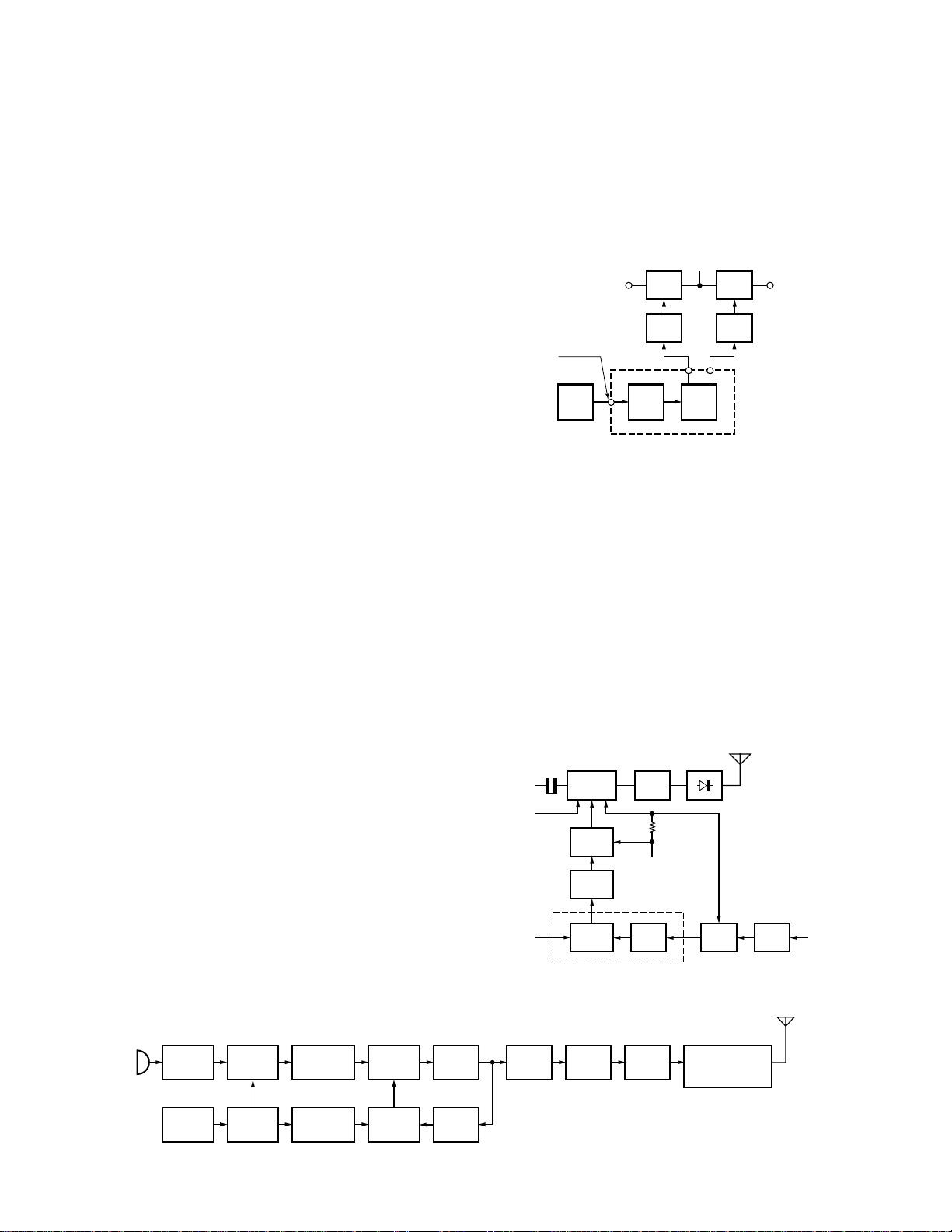
TK-980/98 1
IC508
SHIFT
REG.
IC511
CPU
Q10
SW
Q11
SW
IC300
PLL
Q13
SW
Q12
SW
LD
TX-RX UNIT (B/2)
TR
8C
8R 8T
KEY
PLL lock
: LD “H”
CIRCUIT DESCRIPTION
Transmitter System
■ Outline
The transmitter circuit amplifies the desired frequency. It
FM-modulates the carrier signal by means of a varicap diode.
■ Younger-stage circuit
The signal output from the VCO is amplified by a buffer
amplifier (Q7) and goes to the drive block. The youngerstage circuit provides a stable drive output without a need
for adjustment. The APC circuit controls voltage in the
younger final stage (Q204).
■ VCO/PLL Circuit
The TK-980/981 has a common VCO for the transmitter
and the receiver in a sub-unit (A1). It is housed in a solid
shielded case and connected to the TX-RX unit (A/2) through
CN101. A filtered low-noise power supply is used for the
VCO and varicap diodes.
The VCO is described below. It is designed so that Q101
turns on with a prescribed frequency when a reverse bias is
applied to D100 and D101 by using the control voltage (CV)
through CN101. The control voltage is changed by turning
the trimmer capacitor (TC100). The output from Q103 is applied to the buffer amplifier (Q102) the output from Q102 is
applied to the doubler (Q100) to generate a VCO output signal. This signal is used as a drive input signal or a local signal
of the first mixer. Since a signal output from Q100 is input
to the PLL IC, it passes through CN101 and buffer amplifier
(Q300) and goes to the PLL IC (IC300). The modulation signal from CN101 is applied to D102 and passes through C106
and C107 to modulate the carrier.
The PLL IC uses a fractional N type synthesizer to im-
prove the C/N ratio and lock-up speed. The VCO output signal input to the pin 5 of the PLL IC is divided to produce a
comparison frequency according to a channel step. This signal is compared with the reference frequency which is output from the VCXO (X1). VCXO provides 16.8MHz, 1.5ppm
(–30 to +60°C) and guarantees stable performance when
the temperature changes. The output signal from the phase
comparator passes through a charge pump and an external
active LPF (Q301, Q302) in the PLL IC to generate a DC VCO
control voltage CV. Serial data (DT, CK, EP) are output from
the CPU (IC511) and shift register (IC8) in the TX-RX unit (B/
2) to control the PLL IC. The PLL lock status is always monitored by the CPU.
■ Unlock Circuit
During reception, the TR line goes high, the KEY line
goes low, and Q10 turns on. Q11 turns on and a voltage is
applied to the collector (8R). During transmission, the TR
line goes low, the KEY line goes high and Q13 turns on. Q12
turns on and a voltage is applied to 8T.
The CPU in the TX-RX unit (B/2) monitors the PLL (IC300)
LD line directly. When the PLL is unlocked during transmission, the PLL LD line goes low. The CPU detects this signal
and makes the KEY line low. When the KEY line goes low,
no voltage is applied to 8T, and no signal is transmitted.
Fig. 6 Unlock circuit
■ Power Amplifier Circuit/Final
The transmit output signal from the VCO is amplified to a
specified level of the power module (IC400) by the drive
block (Q202, Q204). The amplified signal goes to a low-pass
filter. The low-pass filter removes unwanted high-frequency
harmonics. The resulting signal passes through the transmission/reception selection diode (D208), then goes to the
antenna terminal.
■ APC Circuit
The direct current that flows through the final module
(IC400) produces a voltage across resistors R127. This voltage is applied to pin 6 of IC13 (2/2), and is input as the reference voltage difference of pin 5 and amplified.
ANT
D20
Q204
IC6
(1/2)
IC400
POWER
AMP
8T
PC
Q19
APC
DRIVER
Q17
PRI
DRIVER
DC
AMP
CURR.
LPF
DET
B
ANT SW
R127
IC13
Q20 Q21
DC
SW
DC
SW
KEY
IC508
Fig. 7 APC circuit
ANT
AF AMP
TA75S01F
MIC KEY
INPUT
26
IC504 IC3 Q101IC711MIC
AF AMP,
IDC, LPF
TC35453F
IC511
CPU
30622M8A
-4F9GP
SUM AMP
TA75W558FU
X1
VCXO
16.8MHz
VCO
2SK508NV
(K52)
IC300
PLL
SA7025DK
Q102
RF AMP
2SC4226
(R24)
Q300
BUFFER
2SC4226
(R24)
Q7
BUFFER
2SC4226
(R24)
Fig. 5 Transmitter system
Q202
RF AMP
2SC3356
(R24)
Q204
RF AMP
2SK2596
IC400
POWER AMP
M67760LC : TK-980
M67760HC : TK-981
Page 27
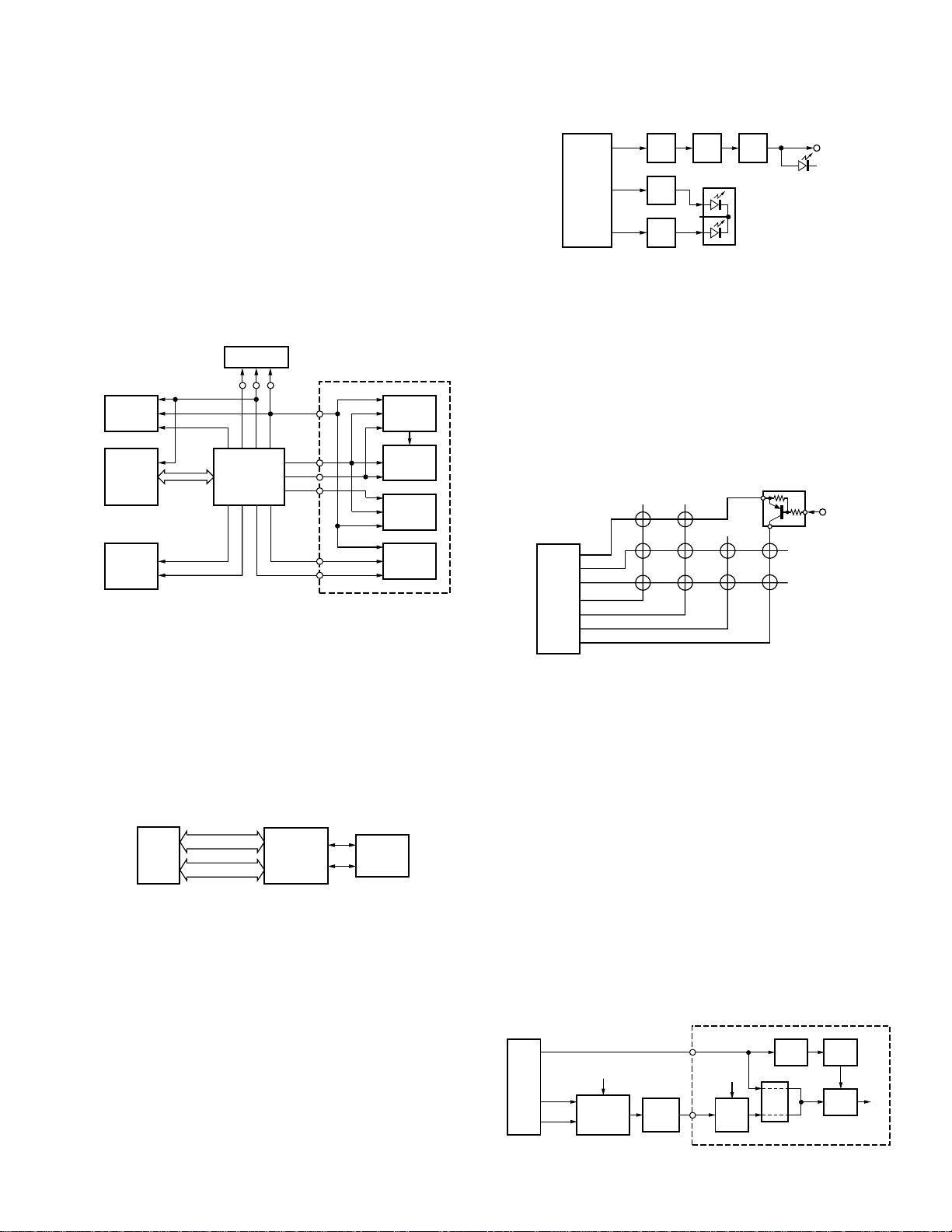
CIRCUIT DESCRIPTION
X1
VCXO
IC5
D/A
A1
VCO
IC3
SUM
AMP
IC506
Analog
SW
IC504
Audio
processor
IC300
PLL
MB
MD
MO
TO
HT
DI
MIC
TX-RX UNIT(A/2)
AFDAT
LSDO
HSDO
IC511
CPU
TK-980/98 1
Control Circuit
The CPU carries out the following tasks:
1) Controls the shift register (IC7, IC8, IC508) AF MUTE, T/R
KEY outputs.
2) Adjusts the AF signal level of the audio processor (IC504)
and turns the filter select compounder on or off.
3) Controls the DTMF decoder (IC507).
4) Controls the LCD assembly display data.
5) Controls the PLL (IC300).
6) Controls the D/A converter (IC5) and adjusts the volume,
modulation and transmission power.
LCD ASSY
TX-RX UNIT (A/2)
IC508
Shift
register
IC504
Audio
processor
IC507
DTMF
DECO.
OECSCK
DT
IC511
ACK
CPU
SD
CP
EP
AFCLR
AFMSKE
AFDAT
AFRDT
AFTRD
AFRTM
AFSTB
Fig. 8 Control circuit
RFCK
ES
EN
IC8
Shift
register
DT
IC7
Shift
register
IC5
D/A
converter
IC300
PLL
Q513
AVR
GRN
RED
LEDA
D512~517
IC508
Shift
register
KBLC
LG
LR
Q512SWQ515
Q508
Q509
SW
D511
SW
SW
Fig. 10 Display circuit
■ Key Matrix Circuit
The TK-980/981 front panel has ten keys. Each of them is
connected to a cross point of a matrix of the KEY1 to KEY7
ports of the microprocessor. The KEY5 to KEY7 ports are
always high, while the KEY1 to KEY4 ports are always low.
The microprocessor monitors the status of the KEY1 to
KEY7 ports. If the state of one of the ports changes, the
microprocessor assumes that the key at the matrix point
corresponding to that port has been pressed. Unused
points (KEY1 to KEY7) are also used for foot switch (FSW)
input.
FSW
IC511
CPU
KEY7
KEY6
KEY5
KEY4
KEY3
KEY2
KEY1
VOLUPVOL
DOWN
MONI A
D SCAN SYS
BC
DOWN
Q511
SYS
UP
■ Memory Circuit
The transceiver has a 2M-bit (256k x 8) flash ROM
(IC510) and an 8k-bit EEPROM (IC512). The flash ROM contains firmware programs, data and user data which is programmed with the FPU. The EEPROM contains adjustment
data. The CPU (IC511) controls the flash ROM through an
external address bus and an external data bus. The CPU
controls the EEPROM through two serial data lines.
CPU
SCL
SDA
IC512
EEPROM
IC510
FLASH
ROM
ADDRESS BUS
DATA BUS
IC511
Fig. 9 Memory circuit
■ Display Circuit
The CPU (IC511) controls the shift register (IC508) and
display LEDs. When the LG line goes high when the transceiver is busy, Q508 turns on and the green LED on D511
lights. In transmit mode, the LR line goes high, Q509 turns
on and the red light lights. Backlighting LEDs for the key
operation unit (D512~D517) and LCD are provided.
When the KBLC line goes high, Q512 turns on, then
Q515 and Q513 turns on, and the key illumination LED
lights. A voltage is applied to the LEDA line to turn on the
LCD backlight.
Fig. 11 Key matrix circuit
■ Encode
The QT, DQT, and LTR signals are output from LSDO of
the CPU (IC511) and go to the D/A converter (IC5) of the TXRX unit (A/2). The DTMF signal is output from HSDO of the
CPU and goes to the audio processor (IC504). An MSK signal is output from the audio processor according to the data
(AFDAT) from the CPU. The signal is summed with a MIC/
MSK signal by the audio processor (IC504), and the resulting
signal passes through an analog switch (IC506) and goes to
the TX-RX unit (A/2) (MO).
MO is summed with the external pin DI line by the summing amplifier (IC3) and the resulting signal goes to the D/A
converter (IC5). The D/A converter (IC5) adjusts the MO
level and the balance between the MO and TO levels. Part
of a TO signal is summed with an output signal from pin 3
(MO) of IC5 and the resulting signal goes to the MD pin of
the VCO. This signal is applied to a varicap diode in the VCO
for direct FM modulation.
Fig. 12 Encode
27
Page 28
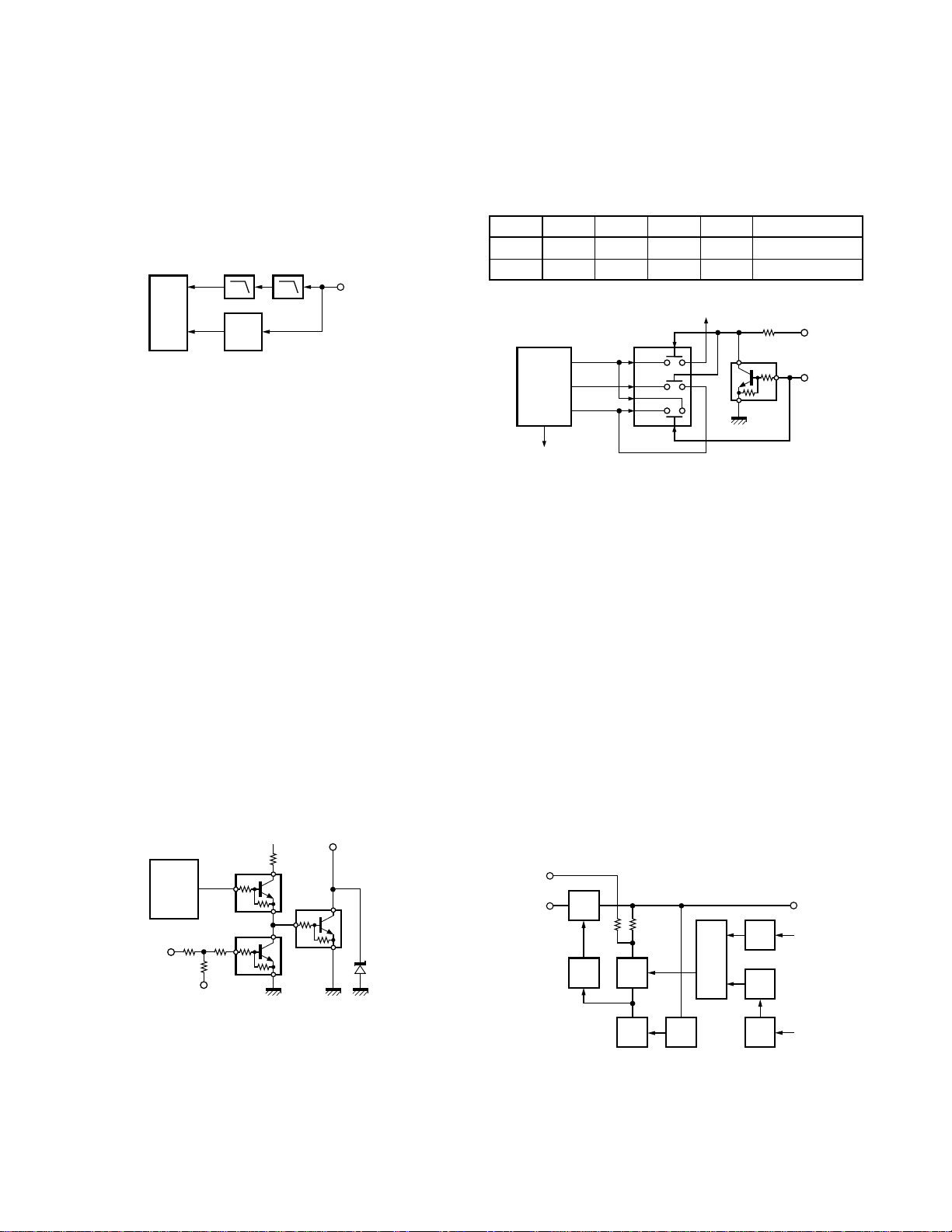
TK-980/98 1
CIRCUIT DESCRIPTION
■ Decode
The signal (DEO) detected by the TX-RX unit (A/2) passes
through two low-pass filters of IC501, goes to LSDI of the
CPU (IC511) to decode QT, DQT, and LTR. The DTMF signal
is decoded by a dedicated IC (IC507) and the resulting signal
is sent to the CPU (IC511) as serial data (STD).
LPF
IC507
DTMF
DECO.
IC501(1/2)
LPF
DEO
IC511
CPU
IC501(2/2)
LSDI
STD
Fig. 13 Decode
■ D/A Converter
The D/A converter (IC5) is used to adjust TONE and MO
modulation, beep, AF volume, TV voltage, FC reference voltage, and PC POWER CONTROL voltage level.
Adjustment values are sent from the CPU as serial data.
The D/A converter has a resolution of 256 and the following
relationship is valid:
D/A output = (Vin – VDAref) / 256 x n + VDAref
Vin : Analog input
VDAref : D/A reference voltage
n : Serial data value from the microprocessor (CPU)
■ Horn Control
The horn switch, consisting of Q4, Q5, and Q6, controls
the horn relay. It is supplied by the dealer to provide the
external horn alert function.
Q5 disables horn alert, turning on when its base is high,
to inhibit the function. Normally, the output from IC7 is low,
and Q6 is off; the base of Q4 is about 0V and Q4 is off.
When horn alert is enabled, the output from IC7 goes high
and Q6 turns on. The base current flows through R58 to Q4
to turn Q4 on. Q4 can sink a maximum of 100mA. If the
operational KAP-1 is used, it can drive up to 2A.
8C
HOR
■ PA Switch
If the optional KAP-1 is used, the PA (Public Address)
function becomes available. In this case, the signal flow
changes as follows;
“PA2” Q507 SW.A SW.B SW.D Public address
LLLHH OFF
HHHL L ON
MO
47K
Q507
5C
“PA2 ”
IC504
Audio
processor
RXOUT
TXOUT
MSKGS
RXIN
IC506
Analog
SW
SW.D
SW.B
SW.A
Fig. 15 PA switch
Power Supply Circuit
When the POWER switch on the TX-RX unit (B/2) is
pressed, the PSW signal goes low. This signal is inverted by
Q26 and sent to a flip-flop IC (IC15). This IC outputs a control signal when the PSW goes low. When the power turns
on, pin 1 of IC15 outputs a low signal and Q30 turns on. The
base of Q28 goes high, Q28 turns on, SB SW (Q27) turns on
and power (SB) is supplied to the set.
This circuit has an over-voltage protection circuit. If a DC
voltage of 20V or higher is applied to the power cable, D34
turns on and a voltage is applied to the base of Q31. This
voltage turns Q31 on and turns Q28 and SBSW off. This
circuit has a TIMED POWER OFF (TOF) function which can
be programmed by software.
It is controlled through pin 6 of IC7. When the TOF line
goes high, Q22 turns on and then Q25 turns on. Pin 6 of
IC15 goes high, then pin 1 goes high to turn Q27 off.
28
Q6
HNC
Q5
R152
+B
Shift
register
IGN
IC7
R2 R50
Fig. 14 Horn control
R58
Q4
D7
IGN
Q27
SB
SW
R152
R151
Q28SWQ30
SW
Q31SWD24
SW
Fig. 16 Power supply circuit
IC15
F. F.
Q26
INV.
Q25
SW
Q22
SW
+B
PSW
TOF
IC7
6pin
Page 29
SEMICONDUCTOR DATA
Microprocessor : 30622M8A-4F9GP (TX-RX Unit (B/2) IC511)
■ Terminal function
Pin No. Name I/O Function
1 LSDOUT O Low speed data output.
2 HSDOUT O High speed data output.
3 HSDIN I High speed data input.
4 DTMSTD I DTMF decode IC data detect input.
5 SELF I Not used.
6 BYTE I +5V.
7 CNVSS I GND.
8 SFTOE O Shift register output enable.
9 LCDCS O LCD driver chip select output.
10 RESET I Microcomputer reset input.
11 XOUT – 9.8304MHz (System clock).
12 VSS – GND.
13 XIN – 9.8304MHz (System clock).
14 VCC – +5V.
15 IGN I Ignition input.
16 AFTRD I MSK modulation data output timing
pulse input.
17 AFRTM I MSK demodulation data input tim-
ing pulse input.
18 MICDAT O MIC key data output.
19 CP O PLL IC clock output.
20 BEEP O Beep data output.
21 AFRDT I MSK demodulation data input.
22 AFREG1 O
23 AFREG2 O
24 EEPDAT O EEPROM data output.
25 EN O D/A converter IC data strobe output.
26 AFCLR O MSK flame reset output.
27 RXCOM2 I External hook input / External serial
28 TXCOM2 I/O External PTT input / External serial
29 TXCOM1 O External serial interface output.
30 RXCOM1 I External serial interface input.
31 LD I PLL unlock detect input.
32 AFMSKE O MSK modulation enable.
33 TXD O Serial interface output.
34 HOOK I Hook input / Serial interface input.
35 AFDAT O MSK data output.
AF IC register switching data output 1.
AF IC register switching data output 2.
interface input.
interface output.
(Enable active “H”)
Pin No. Name I/O Function
36 RFCLK O
37 RDY – Not used.
38 ALE – Not used.
39 HOLD – Not used.
40 HLDA – Not used.
41 BLCK – Not used.
42 RD – Flash memory RD bus.
43 BHE – Not used.
44 WR – Flash memory WR bus.
45 DTMCLK O DTMF decode IC clock output.
46 CNTCLK O
47 EP O PLL IC data strobe output.
48 CSO O Flash memory chip enable.
49 A19 – Not used.
50~59 A18~A9 – Flash memory address bus.
60 VCC – +5V.
61 A8 – Flash memory address bus.
62 VSS – GND.
63~70 A7~A0 – Flash memory address bus.
71~74 KEY1~KEY4 I/O Key matrix data input/output 1~4.
75 MINDAT O Common data output.
76~78 KEY5~KEY7 I Key matrix data input 5~7.
79~86 D7~D0 – Flash memory data bus.
87 DTMDAT I DTMF decode IC data input.
88 AUXDTC I External DTC input.
89 MICBLC O MIC back light control output.
90 POWSW I Power switch input.
91 ANLSQL I Squelch level input.
92 PTT I PTT switch input.
93 RSSI I Received signal strength indicator
94 AVSS – GND.
95 LSDIN I Low speed data input.
96 VREF – +5V.
97 AVCC – +5V.
98 ES1 O Shift register data strobe output.
99 ES2 O Shift register data strobe output.
100 AFSTB O AF IC data strobe output.
TK-980/98 1
Common clock output. (TX-RX unit A/2)
Common clock output. (TX-RX unit B/2)
input (RSSI).
(TX-RX unit B/2)
(TX-RX unit A/2)
29
Page 30
TK-980/98 1
SEMOCONDUCTOR DATA / DESCRIPTION OF COMPONENTS
Shift Register : BU4094BCFV
■ Terminal function (TX-RX unit (B/2) IC508)
Pin No.
■ Terminal function (TX-RX unit (A/2) IC8)
Pin No.
Port Name Function
1 ES ES1 Strobe
2 DT DAT Data
3 CK Clock
4 Q1 LEDR Red LED. H : ON, L : OFF
5 Q2 LEDG Green LED. H : ON, L : OFF
6 Q3 KEYBLT Key back light. H : ON, L : OFF
7 Q4 MMUTE MIC mute. H: Mute, L : Unmute
8 VSS GND
9NC
10 NC
11 Q8 PA2 Public address 2. H : ON, L : OFF
12 Q7 BSHIFT Beat shift. H : ON, L : OFF
13 Q6 KEY TX power switching. H : TX, L : RX
14 Q5 T/R TX/RX switching. H : RX, L : TX
15 OE Output enable
16 VDC +5V
Port Name Function
1 STB ES Strobe
2 SI DT Data
3 CLK CK Clock
4 Q1 AM1 Audio mute 1. H : Mute, L : Unmute
5 Q2 LOK Link complete.
(Programmable active H/L)
6 Q3 POR Buffer amplifier and mixer switch.
H : Normal, L : Power sw on (an instant)
7 Q4 DM Dead mute. H : RX, L : TX
8 VSS GND
9 QS IC7 data output
10 NC
11 Q8 SQ External squelch.
(Programmable active H/L)
12 Q7 CODE2 Option board data 2. H : ON, L : OFF
13 Q6 CODE1 Option board data 1. H : ON, L : OFF
14 Q5 OPT Option board control.
H : ON, L : OFF / Auxiliary B.
(Programmable active H/L)
15 OE Output
16 VDC +5V.
■ Terminal function (TX-RX unit (A/2) IC7)
Pin No.
Port Name Function
1 STB ES Strobe
2 SI DT Data
3 CLK CK Clock
4 Q1 HORN Horn alert. H : ON, L : OFF
5 Q2 H/L
6 Q3 TIMOFF Timed power off. H : Power off
7 Q4 CODE3 Option board data 1. H : ON, L : OFF
8 VSS GND
9NC
10 NC
11 Q8 W/N Wide/Narrow switching. (Not used)
12 Q7 BUSY Trunked system busy.
13 Q6 PA1 Public address 1. H : ON, L : OFF
14 Q5 CODE4 Option board data 1. H : ON, L : OFF
15 OE Output enable
16 VDC +5V
NC
H : Wide, L : Narrow
H : Not busy, L : Busy
DESCRIPTION OF COMPONENTS
TX-RX Unit (X57-6520-XX) (A/2)
-10 : TK-980 -11 : TK-981
Ref. No. Use / Function Operation / Condition
IC1~3 Amplifier
IC4 Switch
IC5 D/A convert
IC6 Amplifier
IC7,8 Shift/store register
IC9 5V AVR
IC10 AF amplifier
IC11 FM demodulation
IC12 5V AVR
IC13 DC amplifier Current detect/PC
IC14 8V AVR
IC15 Power supply logic
circuit control
IC16 9V AVR 8CL
IC300 PLL synthesizer
IC400 Power module RF power 15W
Q1 AF switch
Q2 Ripple filter
30
Page 31
DESCRIPTION OF COMPONENTS
TK-980/98 1
Ref. No. Use / Function Operation / Condition
Q4 DC switch HOR
Q5 DC switch IGN
Q6 DC switch HOR CONT.
Q7 Buffer amplifier
Q8,9 AF mute switch
Q10,11 DC switch 8R
Q12,13 DC switch 8T
Q15 IF amplifier
Q17 APC pre drive APC
Q18 RX mute
Q19 APC drive APC
Q20 Current detector SW TX on
Q21
Q22 DC switch TOF
Q25 DC switch TOF
Q26 DC switch PSW
Q27 SB switch
Q28 DC switch SB
Q30,31 DC switch SB
Q32 AF switch
Q33 DC switch POR. Q7 SW
Q34 Thermal protection SW
Q201 RF amplifier Front amplifier
Q202 RF amplifier Pre drive
Q203 Mixer
Q204 RF amplifier Drive
Q205 DC switch POR. Q203 SW
Q300 RF amplifier PLL input
Q301,302 CP
D1~6 Surge absorption
D7 Voltage reference
D11 DC switch
D16
D17 Surge absorption
D18,19 RF switch TX/RX
D20
D21 Voltage reference
D24 Current protection
D26
D28 Voltage reference
D31
D32 Surge absorption
D34 Voltage reference
D35 Limiter
D37 Reverse protection
Pre current detector SW
Reverse current prevention
Reverse current prevention
Reverse current prevention
Reverse current prevention
TX on
Ref. No. Use / Function Operation / Condition
D200 Limiter Excessive input protection
D208~210 RF switch TX/RX
TX-RX Unit (X57-6520-XX) (B/2)
-10 : TK-980 -11 : TK-981
Ref. No. Use / Function Operation / Condition
IC501~503 Amplifier
IC504 Audio processor
IC506 Analog switch
IC507 DTMF decoder
IC508 Shift/store register
IC509 Reset IC
IC510 Flash ROM
IC511 CPU
IC512 EEPROM
IC513 8V AVR
IC711 Amplifier
Q501 MIC mute
Q502 AF mute
Q503 Amplifier Noise
Q507 DC switch PA
Q508,509 DC switch LED
Q510 Clock shift
Q511 DC switch FSW
Q512 DC switch BLC
Q513 AVR
Q515 DC switch Q513 SW
D501 Surge absorption
D502 Current protection
D503~505 Surge absorption
D507 OR gate MIC mute
D508,509 Limiter
D510
D511~517 Light emission
D518 Voltage reference
D520 Discharge Speed up
PLL/VCO (X58-4530-XX)
Ref. No. Use / Function Operation / Condition
Q100 Buffer amplifier
Q101 VCO
Q102 Doubler
D100,101 VCO control
D102 VCO modulation
Reverse current prevention
back light
-10 : TK-980 -11 : TK-981
31
Page 32
TK-980/98 1
PARTS LIST
CAPACITORS CC 45 TH 1H 220 J
12 3 4 56
1 = Type … ceramic, electrolytic, etc. 4 = Voltage rating
2 = Shape … round, square, ect. 5 = Value
3 = Temp. coefficient 6 = Tolerance
• Temperature coefficient
1st Word C L P R S T U
Color* Black Red Orange Yellow Green Blue Violet
ppm/°C 0 –80 –150 –220 –330 –470 –750
• Tolerance (More than 10pF)
Code C D G J K M X Z P No code
(%) ±0.25 ±0.5 ±2 ±5 ±10 ±20 +40 +80 +100 More than 10µF – 10 ~ +50
–20 –20 –0 Less than 4.7µF –10 ~ +75
• Voltage rating
2nd word
1st word
0 1.0 1.25 1.6 2.0 2.5 3.15 4.0 5.0 6.3 8.0 –
1 10 12.5 16 20 25 31.5 40 50 63 80 35
2 100 125 160 200 250 315 400 500 630 800 –
3 1000 1250 1600 2000 2500 3150 4000 5000 6300 8000 –
ABCDEFGHJ KV
CC45
Color*
2nd Word G H J K L
ppm/°C ±30 ±60 ±120 ±250 ±500
Example : CC45TH = –470 ± 60ppm/°C
• Capacitor value
010 = 1pF
100 = 10pF
101 = 100pF
102 = 1000pF = 0.001µF
103 = 0.01µF
2 2 0 = 22pF
Multiplier
2nd number
1st number
(Less than 10pF)
Code B C D F G
(pF) ±0.1 ±0.25 ±0.5 ±1 ±2
• Chip capacitors
(EX) C C 7 3 F S L 1 H 0 0 0 J
1 234 5 6 7
(Chip) (CH, RH, UJ, SL)
(EX) C K 7 3 F F 1 H 0 0 0 Z
1 234 5 6 7
(Chip) (B, F)
RESISTORS
• Chip resistor (Carbon)
(EX) R D 7 3 E B 2 B 0 0 0 J
1 234 5 6 7
(Chip) (B,F)
• Carbon resistor (Normal type)
(EX) R D 1 4 B B 2 C 0 0 0 J
1 234 5 6 7
1 = Type … ceramic, electrolytic, etc. 5 = Voltage rating
2 = Shape … round, square, ect. 6 = Value
3 = Dimension 7 = Tolerance
4 = Temp. coefficient
32
Refer to the table above.
1 = Type
2 = Shape
3 = Dimension
4 = Temp. coefficient
5 = Voltage rating
6 = Value
7 = Tolerance
Dimension (Chip capacitors)
Dimension code L W T
Empty 5.6 ± 0.5 5.0 ± 0.5 Less than 2.0
A 4.5 ± 0.5 3.2 ± 0.4 Less than 2.0
B 4.5 ± 0.5 2.0 ± 0.3 Less than 2.0
C 4.5 ± 0.5 1.25 ± 0.2 Less than 1.25
D 3.2 ± 0.4 2.5 ± 0.3 Less than 1.5
E 3.2 ± 0.2 1.6 ± 0.2 Less than 1.25
F 2.0 ± 0.3 1.25 ± 0.2 Less than 1.25
G 1.6 ± 0.2 0.8 ± 0.2 Less than 1.0
H 1.0 ± 0.05 0.5 ± 0.05 0.5 ± 0.05
Dimension
L
W
Dimension (Chip resistor)
Dimension code L W T
E 3.2 ± 0.2 1.6 ± 0.2 1.0
F 2.0 ± 0.3 1.25 ± 0.2 1.0
G 1.6 ± 0.2 0.8 ± 0.2 0.5 ± 0.1
H 1.0 ± 0.05 0.5 ± 0.05 0.35 ± 0.05
Rating wattage
Code Wattage Code Wattage Code Wattage
1J 1/16W 2C 1/6W 3A 1W
2A 1/10W 2E 1/4W 3D 2W
2B 1/8W 2H 1/2W
T
Page 33
PARTS LIST
TK-980/98 1
✽ New Parts. indicates safety critical components.
Parts without Parts No. are not supplied.
Les articles non mentionnes dans le Parts No. ne sont pas fournis.
Teile ohne Parts No. werden nicht geliefert.
Address
New
Parts No. Description
parts
Ref. No.
TK-980/981
1 1A A01-2165-23 CABINET UPPER
2 2A A01-2166-23 CABINET LOWER
3 2A A62-0991-03 PANEL ASSY
5 1D B09-0235-05 CAP ACC
6 2B B38-0814-05 LCD ASSY
72D✽ B62-1549-00 INSTRUCTION MANUAL
81C✽ B72-2047-04 MODEL NAME PLATE TK-980
81C✽ B72-1488-24 MODEL NAME PLATE TK-981
10 2B ✽ E23-1136-04 GROUND TERMINAL
11 1C E30-3031-15 ANTENNA CABLE
12 1D E30-3339-05 DC CORD ACC
13 1C E30-3340-05 DC CORD
14 2B E37-0789-05 FLAT CABLE CONT-TX-RX
15 1B ✽ E37-0790-25 LEAD WIRE WITH CONNECTOR SP
17 2B F20-1192-04 INSULATING SHEET
18 1D F51-0016-05 FUSE (6✽30) 6A
20 1B,1C G02-0791-04 FLAT SPRING AF,APC,AVR
21 1B,1C G10-1221-04 FIBROUS SHEET SIDE
22 1B G10-1222-14 FIBROUS SHEET UP,DOWN
23 1A,2B G10-1223-14 FIBROUS SHEET SHIELD CASE
24 1C G13-1468-04 CUSHION DC CORD
25 1B ✽ G13-1873-04 CUSHION SP
26 2C G53-0796-04 PACKING PHONE JACK
28 3D H10-6618-12 POLYSTYRENE FOAMED FIXTURE
29 2E H10-6619-12 POLYSTYRENE FOAMED FIXTURE
30 1D H12-1391-03 INNER PACKING CASE ACC
31 1E H25-0720-04 PROTECTION BAG (200X350)
32 3E H52-1431-02 ITEM CARTON CASE TK-980
32 3E H52-1432-02 ITEM CARTON CASE TK-981
34 2D J19-1584-05 HOLDER ACC
35 1D J29-0627-23 BRACKET ACC
37 2B K29-5284-02 KEY TOP
A 1A,2A N33-2606-45 OVAL HEAD MACHINE SCREW
B 2C N67-3008-46 PAN HEAD SEMS SCREW W
C
D 2B N87-2612-46 BRAZIER HEAD TAPTITE SCREW
39 2D N99-0395-05 SCREW SET ACC
41 1B T07-0246-05 SPEAKER
42 1D T91-0621-05 MICROPHONE ACC
1A,2B,1C
N87-2606-46 BRAZIER HEAD TAPTITE SCREW
Desti-
nation
L : Scandinavia K : USA P : Canada
Y : PX (Far East, Hawaii) T : England E : Europe
Y : AAFES (Europe) X : Australia M: Other Areas
TK-980/981
TX-RX UNIT (X57-6520-XX)
Address
New
parts
Parts No. Description
Ref. No.
C23 C92-0507-05 CHIP-TAN 4.7UF 6.3WV
C24 CC73GCH1H101J CHIP C 100PF J
C25 C92-0507-05 CHIP-TAN 4.7UF 6.3WV
C27 CK73GB1H102K CHIP C 1000PF K
C28 CC73GCH1H220J CHIP C 22PF J
C29 C92-0628-05 CHIP-TAN 10UF 10WV
C30 CK73GB1H102K CHIP C 1000PF K
C31 C92-0628-05 CHIP-TAN 10UF 10WV
C32 CC73GCH1H100D CHIP C 10PF D
C33 CK73GB1E103K CHIP C 0.010UF K
C34 C92-0568-05 CHIP-TAN 22UF 10WV
C35 CC73GCH1H101J CHIP C 100PF J
C36 C92-0628-05 CHIP-TAN 10UF 10WV
C37 C92-1341-05 ELECTRO 100UF 16WV
C38 C92-0507-05 CHIP-TAN 4.7UF 6.3WV
C39 CK73GB1E103K CHIP C 0.010UF K
C40 CC73GCH1H101J CHIP C 100PF J
C41 C92-0628-05 CHIP-TAN 10UF 10WV
C42 C92-0546-05 CHIP-TAN 68UF 6.3WV
C43,44 CC73GCH1H101J CHIP C 100PF J
C45 C92-0507-05 CHIP-TAN 4.7UF 6.3WV
C46 C92-0004-05 CHIP-TAN 1.0UF 16WV
C47 CC73GCH1H101J CHIP C 100PF J
C48 CK73FF1C105Z CHIP C 1.0UF Z
C49 CC73GCH1H101J CHIP C 100PF J
C51 CC73GCH1H101J CHIP C 100PF J
C52 CC73GCH1H100D CHIP C 10PF D
C54 CK73GB1C104K CHIP C 0.10UF K
C55 CC73GCH1H030C CHIP C 3.0PF C
C56 CC73GCH1H101J CHIP C 100PF J
C57 CK73GB1E103K CHIP C 0.010UF K
C58 CC73GCH1H101J CHIP C 100PF J
C59 CC73GCH1H030C CHIP C 3.0PF C
C60 CC73GCH1H101J CHIP C 100PF J
C61 CK73GB1E103K CHIP C 0.010UF K
C62 CC73GCH1H030C CHIP C 3.0PF C
C63 CK73FF1C105Z CHIP C 1.0UF Z
C64 CC73GCH1H101J CHIP C 100PF J
C65 CK73GB1C104K CHIP C 0.10UF K
C66 CK73GB1E103K CHIP C 0.010UF K
C67 CC73GCH1H101J CHIP C 100PF J
C68 CK73GB1C104K CHIP C 0.10UF K
C70 C92-0719-05 ELECTRO 47UF 25WV
C71 CK73GB1C104K CHIP C 0.10UF K
C72,73 CK73GB1H102K CHIP C 1000PF K
Desti-
nation
TX-RX UNIT (X57-6520-XX) -10 : TK-980 -11 : TK-981
D511 B30-2151-05 LED (RED/GRE)
D512-517 B30-2171-05 LED (D)
C1-15 CC73GCH1H101J CHIP C 100PF J
C16 C92-0628-05 CHIP-TAN 10UF 10WV
C18 C92-0507-05 CHIP-TAN 4.7UF 6.3WV
C19 CC73GCH1H100D CHIP C 10PF D
C20-22 CC73GCH1H101J CHIP C 100PF J
C74 C92-0719-05 ELECTRO 47UF 25WV
C75 C92-0044-05 CHIP-ELE 47UF 10WV
C76 CK73GB1H102K CHIP C 1000PF K
C77 C92-0719-05 ELECTRO 47UF 25WV
C78 CK73GB1E103K CHIP C 0.010UF K
C79 C92-0722-05 ELECTRO 470UF 16WV
C80 CK73GB1C104K CHIP C 0.10UF K
C83 CK73FB1H473K CHIP C 0.047UF K
C84 CC73GCH1H120J CHIP C 12PF J TK-980
C84 CC73GCH1H220J CHIP C 22PF J TK-981
33
Page 34
TK-980/981
TX-RX UNIT (X57-6520-XX)
Address
New
Parts No. Description Ref. No.
parts
Ref. No.
C85 CK73GB1H102K CHIP C 1000PF K
C87 CC73GCH1H101J CHIP C 100PF J
C88 CK73GB1E103K CHIP C 0.010UF K
C89 CK73GB1H471K CHIP C 470PF K
C90 CK73GB1H102K CHIP C 1000PF K
PARTS LIST
Destination
C173 CK73GB1E103K CHIP C 0.010UF K
C174 C92-0585-05 CHIP-TAN 4.7UF 16WV
C175 CC73GCH1H101J CHIP C 100PF J
C176 CC73GCH1H470J CHIP C 47PF J TK-980
C176 CC73GCH1H101J CHIP C 100PF J TK-981
Address
New
Parts No. Description
parts
Destination
C91,92 CK73GB1E103K CHIP C 0.010UF K
C94 CK73GB1H471K CHIP C 470PF K
C96 CC73GCH1H180J CHIP C 18PF J
C97 CK73GB1H102K CHIP C 1000PF K
C98 CC73GCH1H150J CHIP C 15PF J
C99 CK73GB1H102K CHIP C 1000PF K
C100 C92-0628-05 CHIP-TAN 10UF 10WV TK-980
C102 CC73GCH1H270J CHIP C 27PF J
C103 CK73GB1C104K CHIP C 0.10UF K
C104 CK73GB1E103K CHIP C 0.010UF K
C105 C92-0004-05 CHIP-TAN 1.0UF 16WV
C106 CK73GB1H102K CHIP C 1000PF K
C107 C92-0628-05 CHIP-TAN 10UF 10WV
C108 CK73GB1C104K CHIP C 0.10UF K
C109,110 CK73GB1H102K CHIP C 1000PF K
C111 CC73GCH1H101J CHIP C 100PF J
C112 CK73GB1H102K CHIP C 1000PF K
C113 CK73GB1E103K CHIP C 0.010UF K
C114 C92-0543-05 CHIP-TAN 3.3UF 10WV
C115 CK73GB1H102K CHIP C 1000PF K
C116 C92-0507-05 CHIP-TAN 4.7UF 6.3WV
C117 CK73GB1E103K CHIP C 0.010UF K
C118 CK73GB1C104K CHIP C 0.10UF K
C121 C92-0543-05 CHIP-TAN 3.3UF 10WV
C123 CK73GB1C104K CHIP C 0.10UF K
C124,125 CK73GB1H102K CHIP C 1000PF K
C126 CK73GB1C104K CHIP C 0.10UF K
C127 CK73GB1E103K CHIP C 0.010UF K
C128,129 CC73GCH1H470J CHIP C 47PF J
C131 CC73GCH1H101J CHIP C 100PF J
C177 C92-0519-05 CHIP-TAN 1.0UF 25WV
C178 CC73GCH1H470J CHIP C 47PF J TK-980
C179 CC73GCH1H101J CHIP C 100PF J TK-981
C195-198 CK73GB1H102K CHIP C 1000PF K
C207 CC73GCH1H101J CHIP C 100PF J
C209 CC73GCH1H101J CHIP C 100PF J
C210 CC73GCH1H030C CHIP C 3.0PF C
C211 CC73GCH1H101J CHIP C 100PF J
C212 CC73GCH1H050C CHIP C 5.0PF C
C213 CC73GCH1H010B CHIP C 1.0PF B
C214,215 CC73GCH1H101J CHIP C 100PF J
C216 CC73GCH1H010B CHIP C 1.5PF B TK-981
C216 CC73GCH1H1R5B CHIP C 1.5PF B TK-980
C217 CK73GB1H102K CHIP C 1000PF K
C218 CC73GCH1H101J CHIP C 100PF J
C219 CC73GCH1H110J CHIP C 11PF J TK-980
C219 CC73GCH1H120J CHIP C 12PF J TK-981
C220 CC73GCH1H101J CHIP C 100PF J
C221 CK73GB1H102K CHIP C 1000PF K
C222 CC73GCH1H101J CHIP C 100PF J
C224 CK73GB1H102K CHIP C 1000PF K
C227 CK73GB1H103K CHIP C 0.010UF K
C228 CK73GB1H102K CHIP C 1000PF K
C229 CK73GB1H103K CHIP C 0.010UF K
C234 CC73GCH1H101J CHIP C 100PF J
C235 CC73GCH1H080D CHIP C 8.0PF D
C236 CC73GCH1H101J CHIP C 100PF J
C240 CK73GB1E103K CHIP C 0.010UF K
C245 CC73GCH1H101J CHIP C 100PF J
C246 C92-0001-05 CHIP C 0.1UF 35WV
C132 CK73GB1C104K CHIP C 0.10UF K
C134 CK73FB1C224K CHIP C 0.22UF K
C136 CK73FB1C224K CHIP C 0.22UF K
C137 CK73GB1H471K CHIP C 470PF K
C142,143 CK73GB1H471K CHIP C 470PF K
C144 CK73GB1H102K CHIP C 1000PF K
C150 CC73GCH1H220J CHIP C 22PF J
C151 CK73GB1H102K CHIP C 1000PF K
C152 C92-0777-05 ELECTRO 1000UF 25WV
C153 CC73GCH1H100D CHIP C 10PF D
C155 CK73GB1H102K CHIP C 1000PF K
C156 CK73GB1E103K CHIP C 0.010UF K
C157 CK73GB1C104K CHIP C 0.10UF K
C158,159 CC73GCH1H040C CHIP C 4.0PF C
C160 CK73GB1C104K CHIP C 0.10UF K
C161 CC73GCH1H101J CHIP C 100PF J
C162 C92-0585-05 CHIP-TAN 4.7UF 16WV
C164 CK73GB1H471K CHIP C 470PF K
C166 CK73GB1C104K CHIP C 0.10UF K
C167 CC73GCH1H100D CHIP C 10PF D
C168 CC73GCH1H080D CHIP C 8.0PF D
C169 CK73GB1H102K CHIP C 1000PF K
C170 CC73GCH1H050C CHIP C 5.0PF C
C171 CC73GCH1H101J CHIP C 100PF J
C172 CK73GB1C104K CHIP C 0.10UF K
34
C247 CC73GCH1H101J CHIP C 100PF J
C249 CC73GCH1H100D CHIP C 10PF D
C251 CC73GCH1H050C CHIP C 5.0PF C TK-981
C251 CC73GCH1H060D CHIP C 6.0PF D TK-980
C252 CK73GB1H102K CHIP C 1000PF K
C253 CC73FCH1H080D CHIP C 8.0PF D TK-981
C253 CC73FCH1H100D CHIP C 10PF D TK-980
C255 CC73FCH1H040C CHIP C 4.0PF C TK-981
C255 CC73FCH1H060D CHIP C 6.0PF D TK-980
C256 CK73GB1H102K CHIP C 1000PF K
C257 C92-0719-05 ELECTRO 47UF 25WV
C258 CK73GB1C104K CHIP C 0.10UF K
C259 C92-0719-05 ELECTRO 47UF 25WV
C260 CK73GB1H102K CHIP C 1000PF K
C261 CK73GB1C104K CHIP C 0.10UF K
C262 C92-0719-05 ELECTRO 47UF 25WV
C263 CK73GB1H102K CHIP C 1000PF K
C264 CK73GB1C104K CHIP C 0.10UF K
C265 C93-0550-05 CHIP C 1.0PF C
C266 C93-0552-05 CHIP C 2.0PF C TK-981
C266 C93-0553-05 CHIP C 3.0PF C TK-980
C267 C93-0568-05 CHIP C 47PF J
C268 CC73FCH1H010C CHIP C 1.0PF C TK-981
C268 CC73FCH1H470J CHIP C 47PF J TK-980
C269 C93-0560-05 CHIP C 10PF D
Page 35
PARTS LIST
Address
New
Parts No. Description Ref. No.
parts
Ref. No.
C271 C93-0550-05 CHIP C 1.0PF C
C272 CC73GCH1H010C CHIP C 1.0PF C
C273 C93-0552-05 CHIP C 2.0PF C TK-981
C273 C93-0553-05 CHIP C 3.0PF C TK-980
C274 CC73GCH1H221J CHIP C 220PF J
Destination
TK-980/98 1
TX-RX UNIT (X57-6520-XX)
New
Address
C531 CK73GB1H562K CHIP C 5600PF K
C533 CK73GB1H562K CHIP C 5600PF K
C535 CK73GB1H102K CHIP C 1000PF K
C536 CC73GCH1H030C CHIP C 3.0PF C
C537 CK73GB1H272K CHIP C 2700PF K
parts
Parts No. Description
Destination
C275 C92-0002-05 CHIP-TAN 0.22UF 35WV
C276 C92-0657-05 CHIP-TAN 2.2UF 20WV TK-981
C276 C92-0754-05 CHIP-TAN 4.7UF 20WV TK-980
C284-286 CC73GCH1H470J CHIP C 47PF J
C289 CK73GB1E103K CHIP C 0.010UF K
C303 C92-0565-05 CHIP-TAN 6.8UF 10WV
C304 CC73GCH1H101J CHIP C 100PF J
C306 CC73GCH1H101J CHIP C 100PF J
C307 CK73GB1H103K CHIP C 0.010UF K
C308 CC73GCH1H2R5B CHIP C 2.5PF B
C309 CC73GCH1H010B CHIP C 1.0PF B
C310 CC73GCH1H1R5B CHIP C 1.5PF B TK-981
C310 CC73GCH1H2R5B CHIP C 2.5PF B TK-980
C313 CC73GCH1H101J CHIP C 100PF J
C314 C92-0001-05 CHIP C 0.1UF 35WV TK-980
C314 C92-0503-05 CHIP C 0.068UF 35WV TK-981
C315 CK73GB1C104K CHIP C 0.10UF K
C317 CC73GCH1H101J CHIP C 100PF J
C318,319 CK73GB1C104K CHIP C 0.10UF K
C320 C92-0003-05 CHIP-TAN 0.47UF 25WV TK-981
C320 C92-0519-05 CHIP-TAN 1.0UF 25WV TK-980
C321 CC73GCH1H040C CHIP C 4.0PF C
C322 C92-0003-05 CHIP-TAN 0.47UF 25WV TK-981
C322 C92-0519-05 CHIP-TAN 1.0UF 25WV TK-980
C325 C92-0003-05 CHIP-TAN 0.47UF 25WV TK-981
C325 C92-0519-05 CHIP-TAN 1.0UF 25WV TK-980
C326 CK73FB1C154K CHIP C 0.15UF K
C327 CC73GCH1H101J CHIP C 100PF J
C328 CK73GB1H471K CHIP C 470PF K
C330 CC73FCH1H101J CHIP C 100PF J
C539 CK73GB1H272K CHIP C 2700PF K
C540 CC73GCH1H271J CHIP C 270PF J
C541 CC73GCH1H151J CHIP C 150PF J
C542 CC73GCH1H271J CHIP C 270PF J
C543 CK73GB1H272K CHIP C 2700PF K
C544 CC73GCH1H030C CHIP C 3.0PF C
C545 CK73GB1H102K CHIP C 1000PF K
C546 CK73GB1H122K CHIP C 1200PF K
C547 CK73GB1H102K CHIP C 1000PF K
C548 C92-0712-05 CHIP-TAN 22UF 6.3WV
C549 CK73GB1C104K CHIP C 0.10UF K
C550 CC73GCH1H101J CHIP C 100PF J
C552 CK73GB1C333K CHIP C 0.033UF K
C553 CK73GB1H472K CHIP C 4700PF K
C554-558 CK73GB1C104K CHIP C 0.10UF K
C559 CK73GB1H102K CHIP C 1000PF K
C560 C92-0507-05 CHIP-TAN 4.7UF 6.3WV
C561 CK73GB1H102K CHIP C 1000PF K
C562,563 CK73GB1H472K CHIP C 4700PF K
C564 CK73GB1E223K CHIP C 0.022UF K
C565 CK73GB1H102K CHIP C 1000PF K
C566 CC73GCH1H101J CHIP C 100PF J
C567 CK73GB1E223K CHIP C 0.022UF K
C568 C92-0712-05 CHIP-TAN 22UF 6.3WV
C569 CC73GCH1H470J CHIP C 47PF J
C570 CK73GB1C104K CHIP C 0.10UF K
C571 CK73GB1H102K CHIP C 1000PF K
C572 CK73FB1H563K CHIP C 0.056UF K
C574 CK73GB1C104K CHIP C 0.10UF K
C575 CK73FB1C334K CHIP C 0.33UF K
C437 CK73GB1H102K CHIP C 1000PF K
C438 CC73GCH1H220J CHIP C 22PF J
C501 CK73GB1H471K CHIP C 470PF K
C503,504 CK73GB1H471K CHIP C 470PF K
C505 CK73GB1C683K CHIP C 0.068UF K
C506 CK73GB1E123K CHIP C 0.012UF K
C509 CK73GB1H222K CHIP C 2200PF K
C510 C92-0507-05 CHIP-TAN 4.7UF 6.3WV
C511 CK73GB1H103K CHIP C 0.010UF K
C512 CK73GB1H471K CHIP C 470PF K
C513 CK73GB1H102K CHIP C 1000PF K
C514 CK73GB1H152K CHIP C 1500PF K
C515 CK73GB1C104K CHIP C 0.10UF K
C516,517 CK73GB1H103K CHIP C 0.010UF K
C518 CK73GB1H102K CHIP C 1000PF K
C519 C92-0507-05 CHIP-TAN 4.7UF 6.3WV
C520 CC73GCH1H121J CHIP C 120PF J
C521,522 CK73GB1C104K CHIP C 0.10UF K
C523 CK73GB1H103K CHIP C 0.010UF K
C524 CK73GB1C104K CHIP C 0.10UF K
C525 CK73GB1H103K CHIP C 0.010UF K
C526 CK73GB1C104K CHIP C 0.10UF K
C527 CK73GB1C333K CHIP C 0.033UF K
C528 CK73GB1H102K CHIP C 1000PF K
C529 CK73GB1H562K CHIP C 5600PF K
C576 CK73GB1C473K CHIP C 0.047UF K
C577 CK73GB1C104K CHIP C 0.10UF K
C578 CK73GB1H103K CHIP C 0.010UF K
C579 CK73GB1H472K CHIP C 4700PF K
C580 CK73GB1H102K CHIP C 1000PF K
C581,582 CK73GB1H103K CHIP C 0.010UF K
C583 CK73GB1H102K CHIP C 1000PF K
C584 CK73GB1H471K CHIP C 470PF K
C592 CK73GB1H102K CHIP C 1000PF K
C593 CK73GB1H103K CHIP C 0.010UF K
C594,595 CC73GCH1H270J CHIP C 27PF J
C596 CC73GCH1H680J CHIP C 68PF J
C597 CK73GB1H103K CHIP C 0.010UF K
C598,599 CC73GCH1H101J CHIP C 100PF J
C600,601 CK73GB1H102K CHIP C 1000PF K
C602 CK73GB1H103K CHIP C 0.010UF K
C603 CK73GB1C104K CHIP C 0.10UF K
C604 C92-0560-05 CHIP-TAN 10UF 6.3WV
C605 CK73GB1H102K CHIP C 1000PF K
C606 CK73GB1H472K CHIP C 4700PF K
C607 CK73GB1C104K CHIP C 0.10UF K
C608 CK73GB1H392K CHIP C 3900PF K
C609,610 CK73GB1H103K CHIP C 0.010UF K
C612 CK73GB1H103K CHIP C 0.010UF K
C613 C92-0606-05 CHIP-TAN 4.7UF 10WV
35
Page 36
TK-980/981
TX-RX UNIT (X57-6520-XX)
Address
New
Parts No. Description Ref. No.
parts
Ref. No.
C614 CK73GB1H102K CHIP C 1000PF K
C616 CK73GB1H102K CHIP C 1000PF K
C617 CC73GCH1H101J CHIP C 100PF J
C620 CC73GCH1H101J CHIP C 100PF J
C622,623 CK73GB1H102K CHIP C 1000PF K
PARTS LIST
Destination
L224 L34-1306-15 AIR-CORE COIL
L225 L92-0179-05 FERRITE CHIP
L226 L40-1078-94 SMALL FIXED INDUCTOR (10NH)
L229 L34-1308-15 AIR-CORE COIL
L300 L40-1563-92 SMALL FIXED INDUCTOR (1.5NH)
Address
New
Parts No. Description
parts
Destination
C624 CC73GCH1H101J CHIP C 100PF J
C625 CK73GB1H102K CHIP C 1000PF K
C626 CC73GCH1H101J CHIP C 100PF J
C627 CK73GB1H102K CHIP C 1000PF K
C628 CC73GCH1H101J CHIP C 100PF J
C630 CK73GB1H102K CHIP C 1000PF K
C631-634 CC73GCH1H101J CHIP C 100PF J
C714 CC73GCH1H331J CHIP C 330PF J
C715 CK73GB1H102K CHIP C 1000PF K
C718 C92-0712-05 CHIP-TAN 22UF 6.3WV
C720 CC73GCH1H470J CHIP C 47PF J
C722,723 CC73GCH1H221J CHIP C 220PF J
C726 CK73GB1C104K CHIP C 0.10UF K
C728 C92-0772-05 CHIP-TAN 10UF 6.3WV
CN1 E40-5737-05 PIN ASSY
CN2 E40-5738-05 PIN ASSY
CN3 E40-3247-05 PIN ASSY
CN4 E40-5738-05 PIN ASSY
CN5 E40-3247-05 PIN ASSY
CN6 E40-3246-05 PIN ASSY
CN7 E40-5982-05 FLAT CABLE CONNECTOR
CN501 E40-5823-05 FLAT CABLE CONNECTOR
CN502 E40-5982-05 FLAT CABLE CONNECTOR
J1 2C E11-0442-05 3.5D PHONE JACK (3P)
J501 1B E08-0877-05 MODULAR JACK
- J31-0543-05 COLLAR (LH-5-1.5)
CF1 L72-0986-05 CERAMIC FILTER TK-981
CF1 L72-0998-05 CERAMIC FILTER TK-980
L1 L40-4795-34 SMALL FIXED INDUCTOR (4.7UH)
L3,4 L40-1875-92 SMALL FIXED INDUCTOR (18NH)
L5 L40-1092-34 SMALL FIXED INDUCTOR
L6 L34-4459-05 COIL
L8 L92-0138-05 FERRITE CHIP
L9 L40-8265-92 SMALL FIXED INDUCTOR (8.2NH)
L10 L40-1092-34 SMALL FIXED INDUCTOR
L11 L40-1091-37 SMALL FIXED INDUCTOR (1.000UH)
L203 L79-1465-05 DIELECTRIC FILTER TK-980
L203 L79-1467-05 DIELECTRIC FILTER TK-981
L205 L40-1075-92 SMALL FIXED INDUCTOR (10NH) TK-981
L205 L40-8265-92 SMALL FIXED INDUCTOR (8.2NH) TK-980
L206 L40-6865-92 SMALL FIXED INDUCTOR (6.8NH) TK-981
L206 L40-8265-92 SMALL FIXED INDUCTOR (8.2NH) TK-980
L207 L79-1465-05 DIELECTRIC FILTER TK-980
L207 L79-1467-05 DIELECTRIC FILTER TK-981
L208 L40-4763-92 SMALL FIXED INDUCTOR (4.7NH)
L209 L40-8265-92 SMALL FIXED INDUCTOR (8.2NH)
L210 L40-3985-45 SMALL FIXED INDUCTOR (0.39UH)
L211 L40-6885-45 SMALL FIXED INDUCTOR (0.68UH)
L218 L40-1078-94 SMALL FIXED INDUCTOR (10NH)
L220 L34-1306-15 AIR-CORE COIL
L221 L34-1317-05 AIR-CORE COIL
L222,223 L34-1307-05 AIR-CORE COIL TK-980
L222,223 L34-1313-05 AIR-CORE COIL TK-981
L301 L40-3963-92 SMALL FIXED INDUCTOR (3.9NH) TK-981
L301 L40-4763-92 SMALL FIXED INDUCTOR (4.7NH) TK-980
L303,304 L40-2763-92 SMALL FIXED INDUCTOR (2.7NH)
L305 L92-0179-05 FERRITE CHIP
L501-508 L92-0138-05 FERRITE CHIP
X1 L77-1882-05 VCXO (16.8MHZ)
X2 L77-1762-05 CRYSTAL RESONATOR (44.395MHZ)
X501 L77-1708-05 CRYSTAL RESONATOR (3.579545MHZ)
X502 L78-0462-05 RESONATOR (9.8304MHz)
XF1 L71-0525-05 MCF (5KHZ) TK-980
XF1 L71-0583-05 MCF (3.75KHZ) TK-981
CP501 R90-0724-05 MULTI-COMP 1K X4
R1 RK73GB1J102J CHIP R 1.0K J 1/16W
R2 R92-1252-05 CHIP R 0 OHM J 1/16W
R3 RK73GB1J101J CHIP R 100 J 1/16W
R4 RK73GB1J102J CHIP R 1.0K J 1/16W
R6,7 R92-1252-05 CHIP R 0 OHM J 1/16W
R8 RK73GB1J102J CHIP R 1.0K J 1/16W
R9 R92-1252-05 CHIP R 0 OHM J 1/16W
R10,11 RK73GB1J102J CHIP R 1.0K J 1/16W
R12 R92-1252-05 CHIP R 0 OHM J 1/16W
R14 RK73GB1J473J CHIP R 47K J 1/16W
R15 RK73GB1J103J CHIP R 10K J 1/16W
R16 RK73GB1J274J CHIP R 270K J 1/16W
R17 R92-1252-05 CHIP R 0 OHM J 1/16W
R19 RK73GB1J153J CHIP R 15K J 1/16W
R20 RK73GB1J104J CHIP R 100K J 1/16W
R21 RK73GB1J563J CHIP R 56K J 1/16W
R22 RK73GB1J104J CHIP R 100K J 1/16W
R23 RK73GB1J224J CHIP R 220K J 1/16W
R25 RK73GB1J394J CHIP R 390K J 1/16W
R26 RK73GB1J104J CHIP R 100K J 1/16W
R27 RK73GB1J473J CHIP R 47K J 1/16W
R28 R92-1252-05 CHIP R 0 OHM J 1/16W
R29 RK73GB1J220J CHIP R 22 J 1/16W
R30 RK73GB1J224J CHIP R 220K J 1/16W
R31 RK73GB1J104J CHIP R 100K J 1/16W
R32,33 RK73GB1J474J CHIP R 470K J 1/16W
R34 R92-1252-05 CHIP R 0 OHM J 1/16W
R36 RK73GB1J103J CHIP R 10K J 1/16W
R37 R92-1252-05 CHIP R 0 OHM J 1/16W
R39 RK73GB1J101J CHIP R 100 J 1/16W
R40 RK73GB1J472J CHIP R 4.7K J 1/16W
R41 RK73GB1J183J CHIP R 18K J 1/16W
R42 RK73GB1J333J CHIP R 33K J 1/16W
R44,45 RK73GB1J154J CHIP R 150K J 1/16W
R46 RK73GB1J104J CHIP R 100K J 1/16W
R47 RK73GB1J473J CHIP R 47K J 1/16W
R48 RK73GB1J122J CHIP R 1.2K J 1/16W
R49 RK73GB1J102J CHIP R 1.0K J 1/16W
R50 RK73GB1J103J CHIP R 10K J 1/16W
R52 RK73GB1J104J CHIP R 100K J 1/16W
R53 R92-1252-05 CHIP R 0 OHM J 1/16W
R54 RK73GB1J154J CHIP R 150K J 1/16W
36
Page 37
Address
New
Parts No. Description Ref. No.
parts
Ref. No.
R55 RK73GB1J104J CHIP R 100K J 1/16W
R56 RK73GB1J103J CHIP R 10K J 1/16W
R57 RK73GB1J473J CHIP R 47K J 1/16W
R58 RK73GB1J102J CHIP R 1.0K J 1/16W
R60 RK73GB1J472J CHIP R 4.7K J 1/16W
PARTS LIST
Destination
R134 RK73GB1J473J CHIP R 47K J 1/16W
R135 R92-1261-05 CHIP R 150 J 1/2W
R137 RK73GB1J473J CHIP R 47K J 1/16W
R139 RK73GB1J102J CHIP R 1.0K J 1/16W
R140 R92-1252-05 CHIP R 0 OHM J 1/16W
Address
New
parts
TK-980/98 1
TX-RX UNIT (X57-6520-XX)
Parts No. Description
Destination
R61 RK73GB1J103J CHIP R 10K J 1/16W
R62 RK73GB1J101J CHIP R 100 J 1/16W
R63-65 R92-1252-05 CHIP R 0 OHM J 1/16W
R66 RK73GB1J682J CHIP R 6.8K J 1/16W
R67 RK73GB1J470J CHIP R 47 J 1/16W
R69 RK73GB1J102J CHIP R 1.0K J 1/16W
R70-73 R92-1252-05 CHIP R 0 OHM J 1/16W
R74 RK73GB1J473J CHIP R 47K J 1/16W
R75 RK73GB1J102J CHIP R 1.0K J 1/16W
R76 RK73GB1J153J CHIP R 15K J 1/16W
R77 RK73GB1J333J CHIP R 33K J 1/16W
R78 RK73GB1J104J CHIP R 100K J 1/16W
R79 RK73GB1J180J CHIP R 18 J 1/16W TK-981
R79 RK73GB1J390J CHIP R 39 J 1/16W TK-980
R80 RK73GB1J473J CHIP R 47K J 1/16W
R82,83 RK73GB1J151J CHIP R 150 J 1/16W TK-980
R82,83 RK73GB1J271J CHIP R 270 J 1/16W TK-981
R85 RK73GB1J122J CHIP R 1.2K J 1/16W
R86,87 R92-1252-05 CHIP R 0 OHM J 1/16W
R88 RK73EB2B181J CHIP R 180 J 1/8W
R89 RK73EB2B151J CHIP R 150 J 1/8W
R90 RK73GB1J2R2J CHIP R 2.2 J 1/16W
R91 RK73GB1J472J CHIP R 4.7K J 1/16W
R92 RK73FB2A472J CHIP R 4.7K J 1/10W
R93 RK73FB2A470J CHIP R 47 J 1/10W
R94 R92-1252-05 CHIP R 0 OHM J 1/16W
R95 RK73FB2A154J CHIP R 150K J 1/10W
R96 RK73GB1J181J CHIP R 180 J 1/16W TK-981
R96 RK73GB1J331J CHIP R 330 J 1/16W TK-980
R97,98 RK73GB1J473J CHIP R 47K J 1/16W
R141 RK73GB1J104J CHIP R 100K J 1/16W
R143 RK73GB1J102J CHIP R 1.0K J 1/16W
R144 RK73GB1J223J CHIP R 22K J 1/16W
R145 RK73GB1J104J CHIP R 100K J 1/16W
R146 R92-1215-05 CHIP R 470 J 1/2W
R148 RK73FB2A472J CHIP R 4.7K J 1/10W
R150 R92-0670-05 CHIP R 0 OHM
R151-153 R92-1252-05 CHIP R 0 OHM J 1/16W
R154 RK73GB1J103J CHIP R 10K J 1/16W
R155 RK73GB1J333J CHIP R 33K J 1/16W
R156 RK73GB1J471J CHIP R 470 J 1/16W
R157 RK73GB1J101J CHIP R 100 J 1/16W
R158,159 R92-1252-05 CHIP R 0 OHM J 1/16W
R160 RK73GB1J184J CHIP R 180K J 1/16W
R163 RK73GB1J104J CHIP R 100K J 1/16W
R166 R92-1252-05 CHIP R 0 OHM J 1/16W
R168 R92-1252-05 CHIP R 0 OHM J 1/16W
R170,171 R92-1252-05 CHIP R 0 OHM J 1/16W
R172 RK73GB1J221J CHIP R 220 J 1/16W
R176 R92-0670-05 CHIP R 0 OHM
R181,182 R92-0679-05 CHIP R 0 OHM
R209 RK73GB1J103J CHIP R 10K J 1/16W
R210 RK73GB1J473J CHIP R 47K J 1/16W
R211 RK73GB1J101J CHIP R 100 J 1/16W
R212 RK73GB1J5R6J CHIP R 5.6 J 1/16W
R214 RK73GB1J221J CHIP R 220 J 1/16W
R217 RK73GB1J101J CHIP R 100 J 1/16W
R218 RK73GB1J473J CHIP R 47K J 1/16W
R219 RK73GB1J273J CHIP R 27K J 1/16W
R220 RK73GB1J473J CHIP R 47K J 1/16W
R99 RK73GB1J152J CHIP R 1.5K J 1/16W
R100 RK73GB1J151J CHIP R 150 J 1/16W TK-981
R100 RK73GB1J331J CHIP R 330 J 1/16W TK-980
R101 RK73FB2A470J CHIP R 47 J 1/10W
R102 RK73FB2A102J CHIP R 1.0K J 1/10W
R103 RK73FB2A223J CHIP R 22K J 1/10W
R104 RK73FB2A473J CHIP R 47K J 1/10W
R105 R92-2538-05 RN 3.9K B 1/8W
R106 R92-1252-05 CHIP R 0 OHM J 1/16W
R107 RK73GB1J473J CHIP R 47K J 1/16W
R109 R92-0670-05 CHIP R 0 OHM
R110 RK73GB1J470J CHIP R 47 J 1/16W
R111 RK73GB1J472J CHIP R 4.7K J 1/16W
R112,113 R92-1268-05 RN 4.7K B 1/8W
R116 RK73GB1J473J CHIP R 47K J 1/16W
R118 RK73GB1J392J CHIP R 3.9K J 1/16W TK-980
R119 RK73GB1J103J CHIP R 10K J 1/16W
R120 R92-1268-05 RN 4.7K B 1/8W
R121 RK73GB1J472J CHIP R 4.7K J 1/16W
R122 RK73FB2A272J CHIP R 2.7K J 1/10W
R124 RK73GB1J223J CHIP R 22K J 1/16W
R127 R92-2680-05 RESISTOR
R128 RK73GB1J223J CHIP R 22K J 1/16W
R129 RK73GB1J100J CHIP R 10 J 1/16W
R132 RK73GB1J104J CHIP R 100K J 1/16W
R221 RK73GB1J153J CHIP R 15K J 1/16W
R223 RK73GB1J102J CHIP R 1.0K J 1/16W
R226 RK73GB1J471J CHIP R 470 J 1/16W
R231 RK73GB1J100J CHIP R 10 J 1/16W
R235 RK73GB1J471J CHIP R 470 J 1/16W
R236 RK73GB1J470J CHIP R 47 J 1/16W
R237 RK73GB1J153J CHIP R 15K J 1/16W
R239 RK73GB1J154J CHIP R 150K J 1/16W
R240 RK73GB1J223J CHIP R 22K J 1/16W
R241 R92-1252-05 CHIP R 0 OHM J 1/16W
R243-245 R92-1252-05 CHIP R 0 OHM J 1/16W
R247 R92-0699-05 CHIP R 10 J 1/2W TK-981
R247 R92-1259-05 CHIP R 18 J 1/2W TK-980
R248,249 R92-1215-05 RESISTOR 470 1/2W TK-981
R248,249 R92-2571-05 RESISTOR 270 1/2W TK-980
R250 RK73GB1J470J CHIP R 47 J 1/16W
R251 RK73GB1J474J CHIP R 470K J 1/16W
R252 R92-1217-05 CHIP R 0 OHM
R253,254 RK73GB1J821J CHIP R 820 J 1/16W
R255,256 R92-1308-05 CHIP R 22 J 1W
R257,258 R92-0670-05 CHIP R 0 OHM
R301-303 RK73GB1J102J CHIP R 1.0K J 1/16W
R305 RK73GB1J103J CHIP R 10K J 1/16W
R306 RK73GB1J471J CHIP R 470 J 1/16W TK-981
R306 RK73GB1J102J CHIP R 1.0K J 1/16W TK-980
37
Page 38
TK-980/981
PARTS LIST
TX-RX UNIT (X57-6520-XX)
Address
New
Parts No. Description Ref. No.
parts
Ref. No.
R307 R92-1252-05 CHIP R 0 OHM J 1/16W
R308 RK73GB1J101J CHIP R 100 J 1/16W
R309 RK73GB1J333J CHIP R 33K J 1/16W TK-980
R309 RK73GB1J154J CHIP R 150K J 1/16W TK-981
R310 RK73GB1J103J CHIP R 10K J 1/16W TK-980
Destination
New
Address
R551 RK73GB1J223J CHIP R 22K J 1/16W
R552 RK73GB1J334J CHIP R 330K J 1/16W
R553 RK73GB1J102J CHIP R 1.0K J 1/16W
R554 RK73GB1J332J CHIP R 3.3K J 1/16W
R555 RK73GB1J394J CHIP R 390K J 1/16W
Parts No. Description
parts
Destination
R310 RK73GB1J473J CHIP R 47K J 1/16W TK-981
R311 RK73GB1J561J CHIP R 560 J 1/16W
R312 RK73GB1J472J CHIP R 4.7K J 1/16W
R313 RK73GB1J273J CHIP R 27K J 1/16W
R314 RK73GB1J103J CHIP R 10K J 1/16W TK-981
R314 RK73GB1J223J CHIP R 22K J 1/16W TK-980
R315 RK73GB1J473J CHIP R 47K J 1/16W
R316,317 R92-1252-05 CHIP R 0 OHM J 1/16W
R318 RK73GB1J391J CHIP R 390 J 1/16W
R319 RK73GB1J102J CHIP R 1.0K J 1/16W
R320 R92-1252-05 CHIP R 0 OHM J 1/16W
R321 RK73GB1J470J CHIP R 47 J 1/16W
R322 RK73GB1J100J CHIP R 10 J 1/16W
R323 R92-1252-05 CHIP R 0 OHM J 1/16W
R408 R92-1252-05 CHIP R 0 OHM J 1/16W
R411 R92-1252-05 CHIP R 0 OHM J 1/16W
R414 R92-1252-05 CHIP R 0 OHM J 1/16W
R502 RK73GB1J184J CHIP R 180K J 1/16W
R503 RK73GB1J223J CHIP R 22K J 1/16W
R504 RK73GB1J184J CHIP R 180K J 1/16W
R505 RK73GB1J102J CHIP R 1.0K J 1/16W
R506 R92-1252-05 CHIP R 0 OHM J 1/16W
R507,508 RK73GB1J154J CHIP R 150K J 1/16W
R512 RK73GB1J122J CHIP R 1.2K J 1/16W
R513 R92-1252-05 CHIP R 0 OHM J 1/16W
R515 RN73GH1J913D CHIP R 91K D 1/16W
R516 RK73GB1J102J CHIP R 1.0K J 1/16W
R518 RN73GH1J333D CHIP R 33K D 1/16W
R519 RN73GH1J913D CHIP R 91K D 1/16W
R520 RN73GH1J683D CHIP R 68K D 1/16W
R556 RK73GB1J223J CHIP R 22K J 1/16W
R558 R92-1252-05 CHIP R 0 OHM J 1/16W
R562 RK73GB1J273J CHIP R 27K J 1/16W
R564 R92-1252-05 CHIP R 0 OHM J 1/16W
R566 RK73GB1J470J CHIP R 47 J 1/16W
R567 RK73GB1J220J CHIP R 22 J 1/16W
R568 RK73GB1J473J CHIP R 47K J 1/16W
R569 RK73GB1J103J CHIP R 10K J 1/16W
R571,572 R92-1252-05 CHIP R 0 OHM J 1/16W
R573 RK73GB1J104J CHIP R 100K J 1/16W
R574 RK73GB1J473J CHIP R 47K J 1/16W
R575 RK73GB1J103J CHIP R 10K J 1/16W
R576 RK73GB1J473J CHIP R 47K J 1/16W
R577 RK73GB1J153J CHIP R 15K J 1/16W
R579 R92-1252-05 CHIP R 0 OHM J 1/16W
R580 RK73GB1J103J CHIP R 10K J 1/16W
R581 RK73GB1J472J CHIP R 4.7K J 1/16W
R582 R92-1252-05 CHIP R 0 OHM J 1/16W
R584 R92-1252-05 CHIP R 0 OHM J 1/16W
R585,586 RK73GB1J473J CHIP R 47K J 1/16W
R587 R92-1252-05 CHIP R 0 OHM J 1/16W
R588 RK73GB1J473J CHIP R 47K J 1/16W
R612 RK73GB1J224J CHIP R 220K J 1/16W
R614 R92-1252-05 CHIP R 0 OHM J 1/16W
R616 RK73GB1J473J CHIP R 47K J 1/16W
R624 R92-1252-05 CHIP R 0 OHM J 1/16W
R633 R92-1252-05 CHIP R 0 OHM J 1/16W
R645 RK73GB1J472J CHIP R 4.7K J 1/16W
R658 RK73GB1J472J CHIP R 4.7K J 1/16W
R667,668 RK73GB1J181J CHIP R 180 J 1/16W
R521 RK73GB1J105J CHIP R 1.0M J 1/16W
R522 RN73GH1J913D CHIP R 91K D 1/16W
R523 RK73GB1J154J CHIP R 150K J 1/16W
R524 RN73GH1J274D CHIP R 270K D 1/16W
R525 RK73GB1J334J CHIP R 330K J 1/16W
R526 RK73GB1J154J CHIP R 150K J 1/16W
R527 RK73GB1J103J CHIP R 10K J 1/16W
R528 RK73GB1J153J CHIP R 15K J 1/16W
R529 R92-1252-05 CHIP R 0 OHM J 1/16W
R530 RK73GB1J394J CHIP R 390K J 1/16W
R531 RK73GB1J473J CHIP R 47K J 1/16W
R532 RK73GB1J334J CHIP R 330K J 1/16W
R533 R92-1252-05 CHIP R 0 OHM J 1/16W
R535 RK73GB1J155J CHIP R 1.5M J 1/16W
R536 RN73GH1J682D CHIP R 6.8K D 1/16W
R537,538 RK73GB1J473J CHIP R 47K J 1/16W
R540 RK73GB1J474J CHIP R 470K J 1/16W
R541 RK73GB1J274J CHIP R 270K J 1/16W
R542 RN73GH1J683D CHIP R 68K D 1/16W
R544 RK73GB1J101J CHIP R 100 J 1/16W
R545 RK73GB1J182J CHIP R 1.8K J 1/16W
R546 RK73GB1J224J CHIP R 220K J 1/16W
R547 RK73GB1J103J CHIP R 10K J 1/16W
R548 RK73GB1J183J CHIP R 18K J 1/16W
R550 RN73GH1J682D CHIP R 6.8K D 1/16W
38
R670 RK73GB1J473J CHIP R 47K J 1/16W
R672,673 RK73GB1J473J CHIP R 47K J 1/16W
R674 RK73FB2A222J CHIP R 2.2K J 1/10W
R675 RK73GB1J472J CHIP R 4.7K J 1/16W
R676 RK73GB1J103J CHIP R 10K J 1/16W
R677 RK73GB1J223J CHIP R 22K J 1/16W
R678 RK73GB1J103J CHIP R 10K J 1/16W
R679 RK73FB2A390J CHIP R 39 J 1/10W
R680 RK73FB2A222J CHIP R 2.2K J 1/10W
R681 RK73GB1J223J CHIP R 22K J 1/16W
R682 RK73GB1J473J CHIP R 47K J 1/16W
R683 RK73GB1J103J CHIP R 10K J 1/16W
R701 RK73GB1J102J CHIP R 1.0K J 1/16W
R702 RK73GB1J101J CHIP R 100 J 1/16W
R705,706 RK73GB1J473J CHIP R 47K J 1/16W
R716 RK73GB1J472J CHIP R 4.7K J 1/16W
R718 RK73GB1J154J CHIP R 150K J 1/16W
R719 RK73GB1J103J CHIP R 10K J 1/16W
R720 RK73GB1J683J CHIP R 68K J 1/16W
R721 RK73GB1J334J CHIP R 330K J 1/16W
R722 RK73FB2A680J CHIP R 68 J 1/10W
R723 R92-1252-05 CHIP R 0 OHM J 1/16W
R724 RK73GB1J392J CHIP R 3.9K J 1/16W
R725 RK73GB1J562J CHIP R 5.6K J 1/16W
R726,727 R92-1252-05 CHIP R 0 OHM J 1/16W
Page 39
Address
New
Parts No. Description Ref. No.
parts
Ref. No.
D1-6 DA204U DIODE
D7 02DZ20(Y,Z) ZENER DIODE
D11 DAN202U DIODE
D16 1SS355 DIODE
D17 DA204U DIODE
PARTS LIST
Destination
Q1 2SK1824 FET
Q2 2SC2412K(S) TRANSISTOR
Q4 DTD114EK DIGITAL TRANSISTOR
Q5,6 DTC114EE DIGITAL TRANSISTOR
Q7 2SC4226(R24) TRANSISTOR
Address
New
parts
TK-980/98 1
TX-RX UNIT (X57-6520-XX)
PLL/VCO (X58-4530-XX)
Parts No. Description
Destination
D18,19 HVC131 DIODE
D20 1SS355 DIODE
D21 02DZ5.6(X,Y) ZENER DIODE
D24 MINISMDC075-02 VARISTOR
D26 1SS355 DIODE
D28 02DZ15(X,Y) ZENER DIODE
D31 1SS355 DIODE
D32 22ZR-10D SURGE ABSORBER
D34 02DZ18(X,Y) ZENER DIODE
D35 MA742 DIODE
D37 DSA3A1 DIODE
D200 HSM88AS DIODE
D208 MA4PH633 DIODE
D209,210 XB15A709 DIODE
D501 DA204U DIODE
D502 MINISMDC075-02 VARISTOR
D503-505 DA204U DIODE
D507 DAN202U DIODE
D508,509 MA742 DIODE
D510 HSC119 DIODE
D518 02DZ9.1(X,Y) ZENER DIODE
D520 MA2S111 DIODE
IC1 TA75W01FU MOS IC
IC2 TC75W51FU MOS IC
IC3 TA75W558FU MOS IC
IC4 TC4S66F MOS IC
IC5 M62363FP MOS IC
IC6 TA75W558FU MOS IC
IC7,8 BU4094BCFV MOS IC
IC9 TA78L05F MOS IC
Q8 DTC363EU DIGITAL TRANSISTOR
Q9 DTA114YUA DIGITAL TRANSISTOR
Q10 DTC114EE DIGITAL TRANSISTOR
Q11 2SA1362(Y) TRANSISTOR
Q12 2SB1132(Q,R) TRANSISTOR
Q13 DTC114EE DIGITAL TRANSISTOR
Q15 2SC2059K(P) TRANSISTOR
Q17 2SC4116(GR) TRANSISTOR
Q18 2SK1824 FET
Q19 2SB1370(E,F) TRANSISTOR
Q20 DTA144EUA DIGITAL TRANSISTOR
Q21 DTC144EUA DIGITAL TRANSISTOR
Q22 DTC114EE DIGITAL TRANSISTOR
Q25,26 DTA114EE DIGITAL TRANSISTOR
Q27 2SA1641(S,T) TRANSISTOR
Q28 DTC114EE DIGITAL TRANSISTOR
Q30 DTA114EE DIGITAL TRANSISTOR
Q31 DTC114EE DIGITAL TRANSISTOR
Q32 2SK1824 FET
Q33 DTC144EE DIGITAL TRANSISTOR
Q34 2SC2712(GR) TRANSISTOR
Q201 2SC4094(R37) TRANSISTOR
Q202 2SC3356(R24) TRANSISTOR
Q203 3SK255 FET
Q204 2SK2596 FET
Q205 DTC144EE DIGITAL TRANSISTOR
Q300 2SC4226(R24) TRANSISTOR
Q301,302 2SC3722K(S) TRANSISTOR
Q501 DTC314TU DIGITAL TRANSISTOR
Q502 DTC144EE DIGITAL TRANSISTOR
IC10 LA4422 BI-POLAR IC
IC11 TA31136FN MOS IC
IC12 TA78L05F MOS IC
IC13 NJM2904E MOS IC
IC14 TA7808S MOS IC
IC15 TC4013BF(N) MOS IC
IC16 NJM78L08UA BI-POLAR IC
IC300 SA7025DK MOS IC
IC400 2C M67760HC HYBRID IC TK-981
IC400 2C M67760LC HYBRID IC TK-980
IC501 TA75W558FU MOS IC
IC502 TC75W51FU MOS IC
IC503 TA75W558FU MOS IC
IC504 TC35453F MOS IC
IC506 BU4066BCFV MOS IC
IC507 LC73872M MOS IC
IC508 BU4094BCFV MOS IC
IC509 RH5VL42C MOS IC
IC510 AT29C020-90TI ROM IC
IC510 W29C020C90 SRAM IC
IC511 30622M8A-4F9GP MPU
IC512 AT2408N10SI2.5 ROM IC
IC512 24LC08BT-ISN ROM IC
IC513 TA78L05F MOS IC
IC711 TA75S01F MOS IC
Q503 2SC4617(S) TRANSISTOR
Q507 DTC144EE DIGITAL TRANSISTOR
Q508,509 2SC4617(S) TRANSISTOR
Q510 2SC4619 TRANSISTOR
Q511 DTA144WE DIGITAL TRANSISTOR
Q512 DTC114EE DIGITAL TRANSISTOR
Q513 2SC2873(Y) TRANSISTOR
Q515 DTC114EE DIGITAL TRANSISTOR
TH1 157-104-55001 THERMISTOR
PLL/VCO (X58-4530-XX) -10 : TK-980 -11 : TK-981
C100 CK73GB1H471K CHIP C 470PF K
C101 CC73GCH1H4R5B CHIP C 4.5PF B TK-981
C101 CC73GCH1H080B CHIP C 8.0PF B TK-980
C102 CC73GCH1HR75C CHIP C 0.75PF C
C103 CK73GB1H471K CHIP C 470PF K
C104 CC73GCH1H1R5B CHIP C 1.5PF B TK-980
C104 CC73GCH1H020B CHIP C 2.0PF B TK-981
C105 CC73GCH1H040B CHIP C 4.0PF B TK-981
C105 CC73GCH1H060B CHIP C 6.0PF B TK-980
C106,107 CC73GCH1HR75B CHIP C 0.75PF B
C108 CK73GB1H102K CHIP C 1000PF K
C109 CC73GCH1H030B CHIP C 3.0PF B
C110 CC73GCH1H050B CHIP C 5.0PF B
39
Page 40
TK-980/981
PARTS LIST
PLL/VCO (X58-4530-XX)
Address
New
Parts No. Description Ref. No.
parts
Ref. No.
C111 CC73GCH1H470J CHIP C 47PF J
C112 CK73GB1H471K CHIP C 470PF K
C113 CC73GCH1H040B CHIP C 4.0PF B TK-980
C113 CC73GCH1H050B CHIP C 5.0PF B TK-981
C114 CK73GB1H471K CHIP C 470PF K TK-981
C114 CK73GB1H102K CHIP C 1000PF K TK-980
C115 CC73GCH1H030B CHIP C 3.0PF B
C116 CC73GCH1H060B CHIP C 6.0PF B
C117 CK73GB1H102K CHIP C 1000PF K
C118 CC73GCH1HR75B CHIP C 0.75PF B
TC100 C05-0384-05 CERAMIC TRIMMER CAP (10P)
CN100 E40-5699-05 PIN ASSY
- F10-2279-04 SHIELDING CASE
L100,101 L40-1595-34 SMALL FIXED INDUCTOR (1.5UH)
L102 L40-1071-35 SMALL FIXED INDUCTOR (10NH) TK-981
L102 L40-1271-35 SMALL FIXED INDUCTOR (12NH) TK-980
L103 L34-4518-05 AIR-CORE COIL
L104 L40-1098-76 SMALL FIXED INDUCTOR (1UH)
Destination
Address
New
Parts No. Description
parts
Destination
L105 L40-1571-35 SMALL FIXED INDUCTOR (15NH) TK-981
L105 L40-3971-35 SMALL FIXED INDUCTOR (39NH) TK-980
L106 L40-1571-35 SMALL FIXED INDUCTOR (15NH) TK-981
L106 L40-2771-35 SMALL FIXED INDUCTOR (27NH) TK-980
L107 L40-1595-34 SMALL FIXED INDUCTOR (1.5UH)
R100,101 R92-1252-05 CHIP R 0 OHM J 1/16W
R102 RK73GB1J102J CHIP R 1.0K J 1/16W
R103 R92-1252-05 CHIP R 0 OHM J 1/16W
R104 RK73GB1J101J CHIP R 100 J 1/16W
R105 RK73GB1J823J CHIP R 82K J 1/16W
R106 RK73GB1J154J CHIP R 150K J 1/16W
R107 RK73GB1J270J CHIP R 27 J 1/16W
R108,109 RK73GB1J101J CHIP R 100 J 1/16W
R110 RK73GB1J181J CHIP R 180 J 1/16W TK-981
R110 RK73GB1J221J CHIP R 220 J 1/16W TK-980
R111 RK73GB1J223J CHIP R 22K J 1/16W
R112 RK73GB1J103J CHIP R 10K J 1/16W
R113 RK73GB1J470J CHIP R 47 J 1/16W
R114 R92-1252-05 CHIP R 0 OHM J 1/16W
D100,101 1SV283 VARIABLE CAPACITANCE DIODE
D102 1SV214 VARIABLE CAPACITANCE DIODE
Q100 2SC4226(R24) TRANSISTOR
Q101 2SK508NV(K52) FET
Q102 2SC4226(R24) TRANSISTOR
40
Page 41
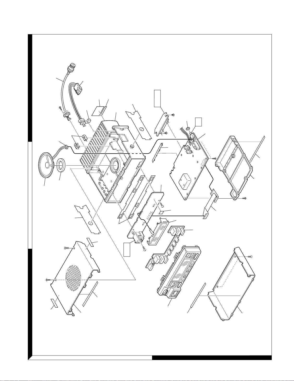
EXPLODED VIEW
1
2
A
B
C
41
25
21
23
1
11
20x2
15
24
13
8
701
21
702
703
703
22x2
J501
17
6
37
3
23
2
23
704
14
26
J1
10
IC400
Cx2
B
B
Cx2
Dx11
C
C
A
A
Ax2
TX-RX unit (A/2)
TX-RX unit
(B/2)
A M2.6 x 6 (OC) BLK : N33-2606-45
B M3 x 8 : N67-3008-46
C M2.6 x 6 (Br-Tap) : N87-2606-46
D M2.6 x 12 (Br-Tap) : N87-2612-46
TK-980/98 1
Parts with the exploded numbers larger than 700 are not supplied.
41
Page 42
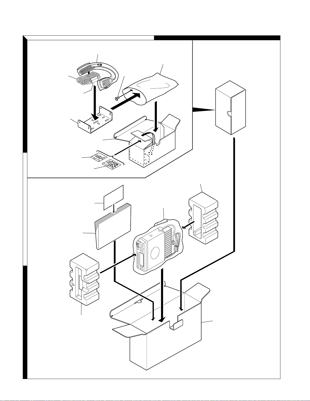
TK-980/98 1
PACKING
12 DC cord
(E30-3339-05)
1
35 Bracket
(J29-0627-23)
18 Fuse
(F51-0016-05) x 2
30 Inner packing case
(H12-1391-03)
34 Holder
(J19-1584-05)
39 Screw set
(N99-0395-05)
D
42 Microphone
(T91-0621-05)
E
31 Protection bag
(H25-0720-04)
5 Cap
(B09-0235-05)
29 Polystyrene foamed fixture
(H10-6619-12)
705 Warranty card
2
7 Instruction manual
(B62-1549-00)
3
28 Polystyrene foamed fixture
(H10-6618-12)
31 Protection bag
(H25-0720-04)
32 Item carton case
(H52-1431-02) : TK-980
(H52-1432-02) : TK-981
42
Parts with the exploded numbers larger than 700 are not supplied.
Page 43
ADJUSTMENT
TK-980/98 1
Test Mode
■ Test Mode Operating Features
This transceiver has a test mode.
press [A] key and turn power on. Hold [A] key until test
channel No. and test signalling No. appears on LCD.
Test mode can be inhibited by programming. To exit test
mode, switch the power on again. The following functions
are available in test mode.
• Controls (“FCN” appears)
[PTT] Used when making a transmission.
[MON] Monitor on and off.
[SCN] MSK 1200bps and 2400bps.
[A] Function off.
[B] Compander function on and off.
[C] Talk around on and off.
[D] Function off.
[System Up/Down] Changes channel
[Volume Up/Down] Volume up/down.
• Controls (“FCN” not appears)
[PTT] Used when making a transmission.
[MON] Monitor on and off.
[SCN] Sets to the tuning mode.
[A] Function on.
[B] None.
[C] Changes signalling.
[D] None.
[System Up/Down] Changes channel
[Volume Up/Down] Volume up/down.
Note : If a [SCN], [A], [B], [C] key is pressed during transmission, the DTMF corresponding to the key that was pressed
is sent.
• LCD indicator
“SCN” Unused
“
” Lights at compander on.
“AUX” Unused.
“P” Unused.
“MON” Lights at monitor on.
“SVC” Unused.
“
” Lights at MSK 2400bps.
• LED indicator
Red LED Lights during transmission.
Green LED Lights when there is a carrier.
• Sub LCD indicator
“FCN” Appears at function on.
■ Frequency and Signalling
The set has been adjusted for the frequencies shown in
the following table. When required, re-adjust them following the adjustment procedure to obtain the frequencies you
want in actual operation.
To enter test mode,
• Frequency (MHz)
Channel TK-980 TK-981
No. RX (TX : TA) TX RX (TX : TA) TX
1 851.05000 806.05000 935.0250 896.0250
2 851.55000 806.55000 935.0500 896.0500
3 860.00000 815.00000 938.0000 899.0000
4 860.50000 815.50000 938.0250 899.0250
5 865.98750 820.98750 939.9875 900.9875
6 869.40000 824.40000 940.4000 901.4000
7 869.90000 824.90000 940.9000 901.9000
8 855.40000 810.40000 936.2500 897.2500
9 865.60000 820.60000 939.3000 900.3000
10 867.50000 822.50000 936.7500 897.7500
11~16 ––––
• Signalling
Signalling No. RX TX
1 None None
2 None 100Hz square
3 LTR data LTR data
4 QT 67.0Hz QT 67.0Hz
5 QT 151.4Hz QT 151.4Hz
6 QT 210.7Hz QT 210.7Hz
7 QT 250.3Hz QT 250.3Hz
8 DQT D023N DQT D023N
9 DQT D754I DQT D754I
10 DTMF DEC, (159D) DTMF ENC, (159D)
11 None DTMF tone
12 None None
13 None Single tone 1200Hz
14 None MSK
15 MSK code MSK code
Note : In test mode, if the operation frequency is in NPSPAC
band (e.g. SYS 10), all deviations are automatically changed
as the system deviation becomes ±4kHz.
• Preparations for tuning the transceiver
Before attempting to tune the transceiver, connect the
unit to a suitable power supply.
Whenever the transmitter is turned, the unit must be
connected to a suitable dummy load (i.e. power meter).
The speaker output connector must be terminated with a
4Ω dummy load and connected to an AC voltmeter and an
audio distortion meter or a SINAD measurement meter at all
times during tuning.
• Transceiver tuning
(To place transceiver in tuning mode)
Channel appears on LCD. Set channel according to tun-
ing requirements.
LCD display (Test mode)
–
11
Channel No. Signalling No.
43
Page 44
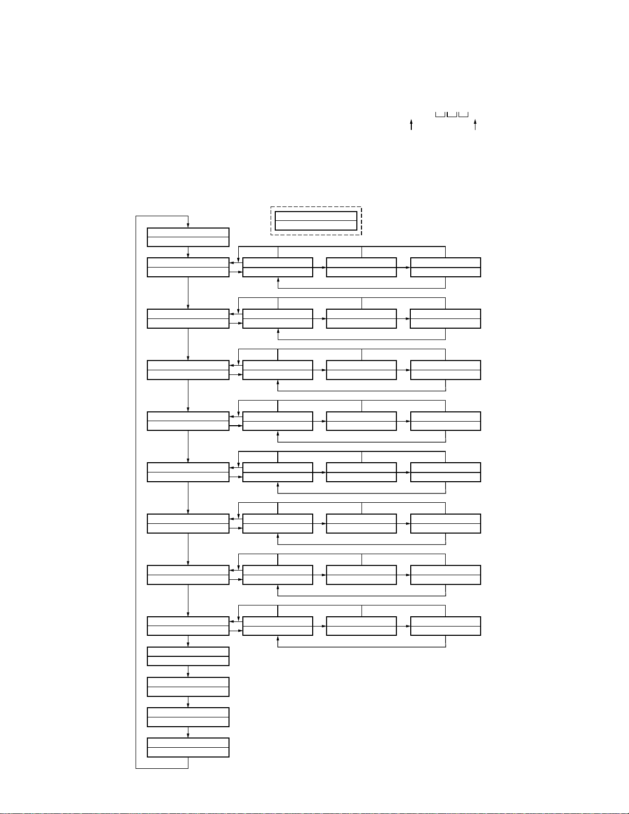
TK-980/98 1
ADJUSTMENT
Press [SCN], now in tuning mode. Use [B] button to
write tuning data through tuning modes, and [System Up/
Down] : to adjust tuning requirements (1 to 256 appears on
LCD).
Use [C] button to select the adjustment item through tuning modes. Use [A] button to adjust 3-point tuning.
■ Tuning Mode
FREQ 256
Frequency adj.
[C]
POW 256
Power
[C]
TPOW 256
TA power
[C]
MAX 256
Max deviation
[C]
[A]
[A]
[A]
[A] [A] [A]
L POW 256
Power (Low)
[C]
[A] [A] [A]
L TPOW 256
TA power (Low)
[C] [C]
[A] [A] [A]
L MAX 256
Max deviation (L)
[C] [C]
LCD display (Tuning mode)
Display
Function name
C POW 256
Power (Cen)
[C]
C TPOW 256
TA power (Cen)
[C]
C MAX 256
Max deviation (C)
[C]
FREQ 1
Adjustment item Adjustment (1~256)
H POW 256
Power (Hi)
[C]
[C]
[C]
[C]
H TPOW 256
TA power (Hi)
H MAX 256
Max deviation (H)
NMAX 256
Max deviation (NPSPAC TK-980)
[C]
BAL 256
DQT balance
[C]
FQT 256
Fine QT
[C]
FDQT 256
Fine DQT
[C]
FLTR 256
Fine LTR
[C]
DTMF 256
DTMF deviation
[C]
FMSK 256
MSK deviation
[C]
TONE 256
Tone deviation
[C]
SQL 256
Squelch (Wide)
[C]
L NMAX 256
Max deviation (NPSPAC) (L)
[A]
L BAL 256
DQT balance (L)
[A]
L FQT 256
Fine QT (L)
[A]
L FDQT 256
Fine DQT (L)
[A]
L FLTR 256
Fine LTR (L)
[A]
[A] [A] [A]
C NMAX 256
Max deviation (NPSPAC) (C)
[C] [C]
[A] [A] [A]
[C] [C]
[A] [A] [A]
[C] [C]
[A] [A] [A]
[C] [C]
[A] [A] [A]
[C] [C]
[C]
DQT balance (C)
[C]
[C]
[C]
[C]
C BAL 256
C FQT 256
Fine QT (C)
C FDQT 256
Fine DQT (C)
C FLTR 256
Fine LTR (C)
H NMAX 256
Max deviation (NPSPAC) (H)
[C]
H BAL 256
DQT balance (H)
[C]
H FQT 256
Fine QT (H)
[C]
H FDQT 256
Fine DQT (H)
[C]
H FLTR 256
Fine LTR (H)
[C]
44
Page 45
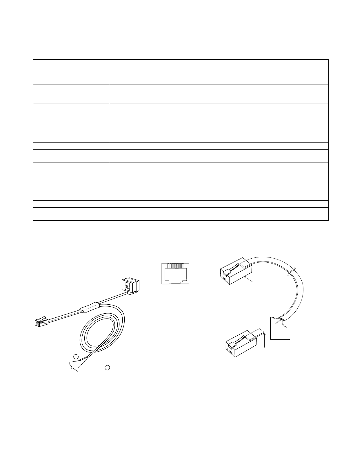
TK-980/98 1
1
8
Cut
E30-3382-05
PTT (TXD) BLK
ME (GND) RED
HOOK (RXD) YEL
ADJUSTMENT
Test Equipment Required for Alignment
Test Equipment Major Specifications
1. Standard Signal Generator Frequency Range 806 to 870MHz (TK-980), 896 to 941MHz (TK-981)
(SSG) Modulation Frequency modulation and external modulation
Output –127dBm/0.1µV to greater than –7dBm/100mV
2. Power Meter Input Impedance 50Ω
Operation Frequency 806 to 870MHz or more (TK-980), 896 to 941MHz (TK-981)
Measurement Capability Vicinity of 30W
3. Deviation Meter Frequency Range 806 to 870MHz (TK-980), 896 to 941MHz (TK-981)
4. Digital Volt Meter Measuring Range 1 to 16V DC
(DVM) Accuracy High input impedance for minimum circuit loading
5. Oscilloscope DC through 30MHz
6. High Sensitivity Frequency Range 10Hz to 1000MHz
Frequency Counter Frequency Stability 0.2ppm or less
7. Ammeter 10A
8. AF Volt Meter Frequency Range 50Hz to 10kHz
(AF VTVM) Voltage Range 3mV to 3V
9. Audio Generator (AG) Frequency Range 50Hz to 5kHz or more
Output 0 to 1V
10. Distortion Meter Capability 3% or less at 1kHz
Input Level 50mV to 10Vrms
11. Voltmeter Measuring Range 1.5 to 30V DC or less
Input Impedance 50kΩ/V or greater
12. 4Ω Dummy Load Approx. 4Ω, 4W
13. Regulated Power Supply 13.6V, approx. 10A (adjustable from 9 to 17V)
Useful if ammeter requipped
Tuning cable (E30-3383-05)
MIC connector
Test cable for microphone input
(Front view)
Adapter cable (E30-3383-05) is required for
injecting an audio if PC tuning is used.
See “PC Mode” section for the connection.
Lead wire +
MIC
Shiel wire –
8
1
1 : BLC
2 : PSB
3 : E
4 : PTT
5 : ME
6 : MIC
7 : HOOK
8 : CM
45
Page 46
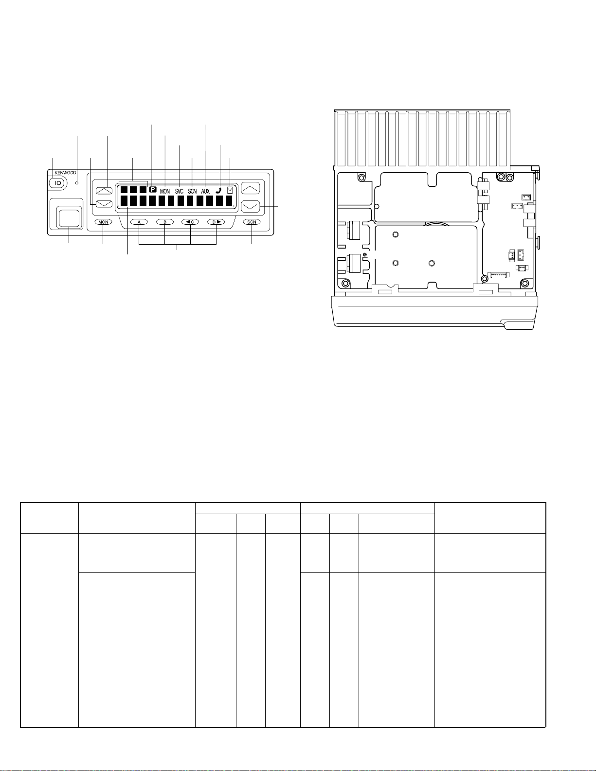
TK-980/98 1
TX-RX UNIT (A/2)
PLL/VCO
TP1
TC100
L6
ADJUSTMENT
Adjustment Location
■ Switch
BUSY/
TX LED
POWER
MODULAR
MIC JACK
VOLUME
UP
VOLUME
DOWN
MONITOR
ALPHANUMERIC
PRIORITY
MONITOR
SUB
DISPLAY
DISPLAY
■ Note
• Flash memory
The firmware program (User mode, Test mode, Tuning
mode, etc.) and the data programmed by the FPU (KPG-49D)
for the flash memory, is stored in memory. When parts are
changed, program the data again.
• EEPROM
The tuning data (Deviation, Squelch, etc.) for the
EEPROM, is stored in memory. When parts are changed,
readjust the transceiver.
AUXILIAY
SERVICE
PROGRAMMABLE
FUNCTION KEYS
HANDSET
SCAN MAIL
SCAN
■ Adjustment Point
SYSTEM
UP
SYSTEM
DOWN
■ Repair Jig (Chassis)
Use jig (Part No. : A10-4010-02) for repairing the
TK-980/981. The jig facilitates the voltage check
when the voltage on the component side TX-RX unit
(A/2) is checked during repairs.
Common Section
Measurement
Test-
equipment
1. PLL lock 1) Set test mode DVM TX-RX TP1 PLL TC100 1.5V ±0.1V
voltage CH : (TA) CH7 - Sig1
PTT : ON (Transmit) F. conter
2) CH : CH1 - Sig1 Check 6.6V or less
PTT : ON (Transmit)
Power meter
Unit Terminal
(A/2)
Unit Parts Method
46
Adjustment
Specifications/RemarksConditionItem
Page 47
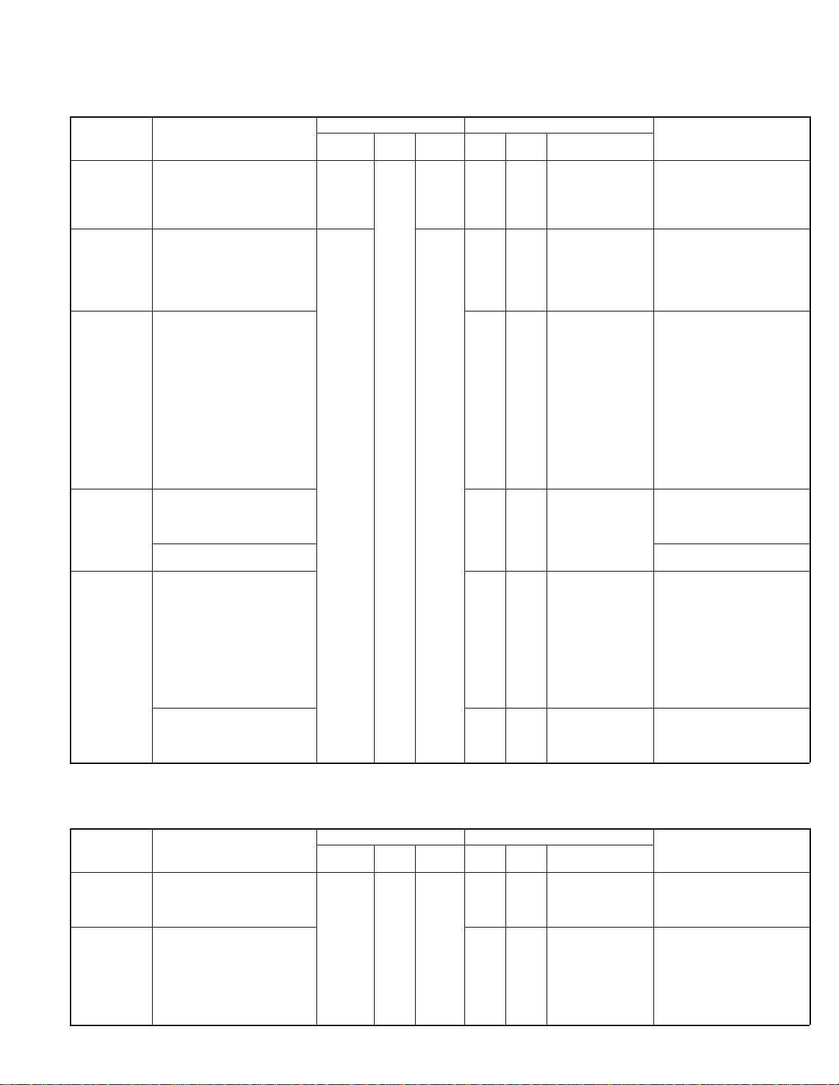
TK-980/98 1
ADJUSTMENT
Receiver Section
Measurement
Test-
equipment
1.
Discriminator
2. Sensitivity 1) Set test mode SSG ANT Check 12dB SINAD or more.
check
3. Squelch 1) Set test mode AG Squelch closed
1) Set test mode SSG Rear ANT TX-RX L6
CH : CH4 - Sig1 panel (A/2)
SSG output : –53dBm AF VTVM ACC
AF : 1.4V/4Ω
CH : CH1 - Sig 1
SSG output : –116dBm AF VTVM ACC
SSG MOD : 3kHz Distortion (EXT.SP)
AF output : 1V/4Ω meter
CH : CH4 - Sig 1 once.
Select “SQL” in tuning mode.
SSG freq’ be opened.
: 860.5MHz (TK-980)
: 938.025MHz (TK-981)
SSG output : Value when 2dB
is subtracted from the
sensitivity value of 12dB
SINAD.
SSG MOD : 3kHz (TK-980)
1.5kHz (TK-981)
Oscilloscope
Oscilloscope
Unit Terminal
(EXT.SP)
Unit Parts Method
Adjustment
Specifications/RemarksConditionItem
AF output maximum.
.
Then squelch must
4. Squelch 1) Set test mode Check Squelch must be opened.
check CH : CH4 - Sig1
SSG output :
2) SSG output : OFF Squelch must be closed.
5. QT check 1) Set test mode
CH : CH4 - Sig5
SSG MOD
INT : 1kHz
EXT : 151.4Hz
SSG system MOD DEV
: ±3.75kHz (TK-980)
: ±1.85kHz (TK-981)
SSG output :
2) CH : CH1 - Sig4 Check Squelch must be closed.
CH1 - Sig6
CH1 - Sig7
12dB SINAD level
10dB SINAD level
Transmitter Section
1. Frequency 1) Set test mode
Select “FREQ” in tuning mode.
PTT : ON
Measurement
Test-
equipment
Power meter
F. counter panel 896.025MHz±100Hz (TK-981)
Unit Terminal
Rear ANT Check 806.050MHz±100Hz (TK-980)
Unit Parts Method
Adjustment
Specifications/RemarksConditionItem
2. Maximum 1) Set test mode Check 16.0W or more.
power check
Select “H POW” in tuning mode.
“POW 256”
PTT : ON
.
47
Page 48
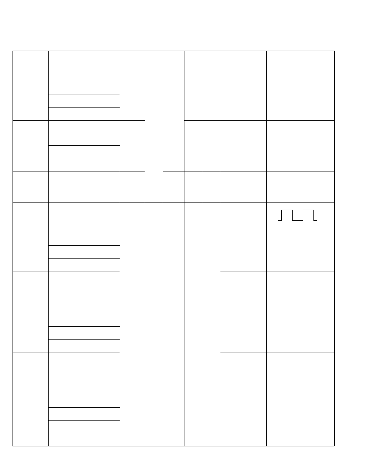
TK-980/98 1
ADJUSTMENT
Measurement
Test-
equipment
3. High power 1) Set test mode
Select “POW” in tuning mode.
“L POW”
PTT : ON
2) “C POW”
PTT : ON
3) “H POW”
PTT : ON
4. TA power 1) Set test mode
Select “L POW” in tuning mode.
“L TPOW”
PTT : ON
2) “C TPOW”
PTT : ON
3) “H TPOW”
PTT : ON
5. Power check 1) Set test mode
CH : CH1 - Sig1 7A or less
CH4 - Sig1 Ammeter DC IN
CH7 - Sig1
PTT : ON
6. Modulation 1) Set test mode
balanced MIC input : OFF Deviation panel modulation
Select “BAL” in tuning mode. meter waveform neat.
“L BAL”
Deviation meter filter
LPF : 3kHz, HPF : OFF AF VTVM Front MIC
De-emphasis : OFF AG panel
2) “C BAL”
PTT : ON
3) “H BAL”
PTT : ON
7. Maximum 1) Set test mode 3.8kHz (TK-980) ±50Hz
deviation
8. NPSPAC 1) Set test mode 2.9kHz (TK-980) ± 50Hz
maximum
deviation
Connect AG to the MIC terminal.
Select “MAX” in tuning mode.
“L MAX” larger +, –)
AG : 1kHz/50mV
Deviation meter filter
LPF : 15kHz, HPF : OFF
De-emphasis : OFF
PTT : ON
2) “C MAX”
PTT : ON
3) “H MAX”
PTT : ON
Connect AG to the MIC terminal.
Select “NMAX” in tuning mode.
“L NMAX”
AG : 1kHz/50mV
Deviation meter filter
LPF : 15kHz, HPF : OFF
De-emphasis : OFF
PTT : ON
2) “C NMAX”
PTT : ON
3) “H NMAX”
PTT : ON
Power meter
F. counter panel
Power meter
Power meter
Power meter
Oscilloscope
Unit Terminal
Rear ANT 15.0W ±1.0W
ANT Check 15W±1W
Rear ANT Make the de-
Unit Parts Method
Adjustment
Specifications/RemarksConditionItem
13.0W ±1.0W
1.75kHz (TK-981)
(According to the
(According to the
larger +, –)
48
Page 49
ADJUSTMENT
TK-980/98 1
Measurement
Test-
equipment
9. MIC 1) Set test mode
sensitivity CH : CH4 - Sig1 Deviation panel 1.1~1.9kHz (TK-981)
check AG : 1kHz/5mV meter
PTT : ON
10. QT 1) Set test mode 0.75kHz (Tk-980) ±50Hz
deviation Select “FQT” in tuning mode. AF VTVM Front MIC 0.35kHz (TK-981)
“L FQT” AG panel
Deviation meter filter
LPF : 3kHz
HPF : OFF
PTT : ON
2) “C FQT”
PTT : ON
3) “H FQT”
PTT : ON
11. DQT 1) Set test mode 0.75kHz (TK-980) ±50Hz
deviation
12. Fine LTR 1) Set test mode 1.0kHz (TK-980) ±50Hz
13. DTMF 1) Set test mode 3.0kHz (TK-980) ±0.2kHz
deviation
14. MSK 1) Set test mode 3.0kHz (TK-980) ±0.1kHz
deviation
15. TONE 1) Set test mode 3.0kHz (TK-980) ±0.1kHz
deviation
Select “F DQT” in tuning mode.
“L FDQT”
Deviation meter filter
LPF : 3kHz
HPF : OFF
PTT : ON
2) “C FDQT”
PTT : ON
3) “H FDQT”
PTT : ON
Select “FLTR” in tuning mode.
“L FLTR”
deviation meter filter
LPF : 3kHz
HPF : OFF
PTT : ON
2) “C FLTR”
PTT : ON
3) “H FLTR”
PTT : ON
Select “DTMF” in tuning mode.
Deviation meter filter
LPF : 15kHz
HPF : OFF
PTT : ON
Select “FMSK” in tuning mode.
Deviation meter filter
LPF : 15kHz
HPF : OFF
PTT : ON
Select “TONE” in tuning mode.
Deviation meter filter
LPF : 15kHz
HPF : OFF
PTT : ON
Power meter
Oscilloscope
Unit Terminal
Rear ANT Check 2.2~3.8kHz (TK-980)
Unit Parts Method
Adjustment
Specifications/RemarksConditionItem
0.35kHz (TK-981)
0.75kHz (TK-981)
1.5kHz (TK-981)
1.5kHz (TK-981)
1.5kHz (TK-981)
49
Page 50
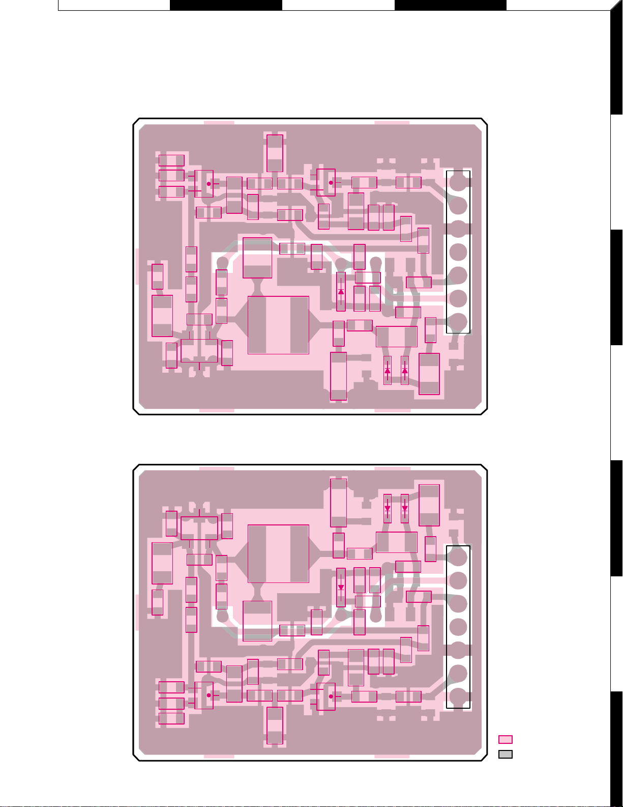
A
PC BOARD VIEWS TK-980/98 1
PLL/VCO (X58-4530-XX) -10 : TK-980 -11 : TK-981 Component side view
DB
EC
1
R108
C117
R112
R110
L107
C116
Q102
R113
C118
C113
S
R111
G
D
Q101
C106
C107
C110
L106
C115
C114
L104
L105
L103
C109
R109
R107
Q100
R105
C112
D102
C105
TC100
C104
L102
R106
R102
C102
C101
C111
C100
D101
C108
L101
R114
R104
R101
C103
D100
J72-0608-02
CN100
OUT
R103
NC
8CL
MD
R100
CV
L100
2
E
E
3
4
PLL/VCO (X58-4530-XX) -10 : TK-980 -11 : TK-981
Foil side view
C112
R105
Q100
TC100
C105
D102
C101
C102
R102
R106
L102
C104
D101
C100
C111
D100
L101
C103
R101
R103
R104
C108
R114
L107
R110
R112
C117
R108
C116
S
C113
C118
R113
Q102
G
R111
Q101
D
C110
C107
C106
L106
L104
C114
C115
L103
R107
R109
C109
L105
L100
R100
CV
MD
8CL
NC
E
OUT
E
CN100
5
6
J72-0608-02
Component side
Foil side
7
50
Page 51
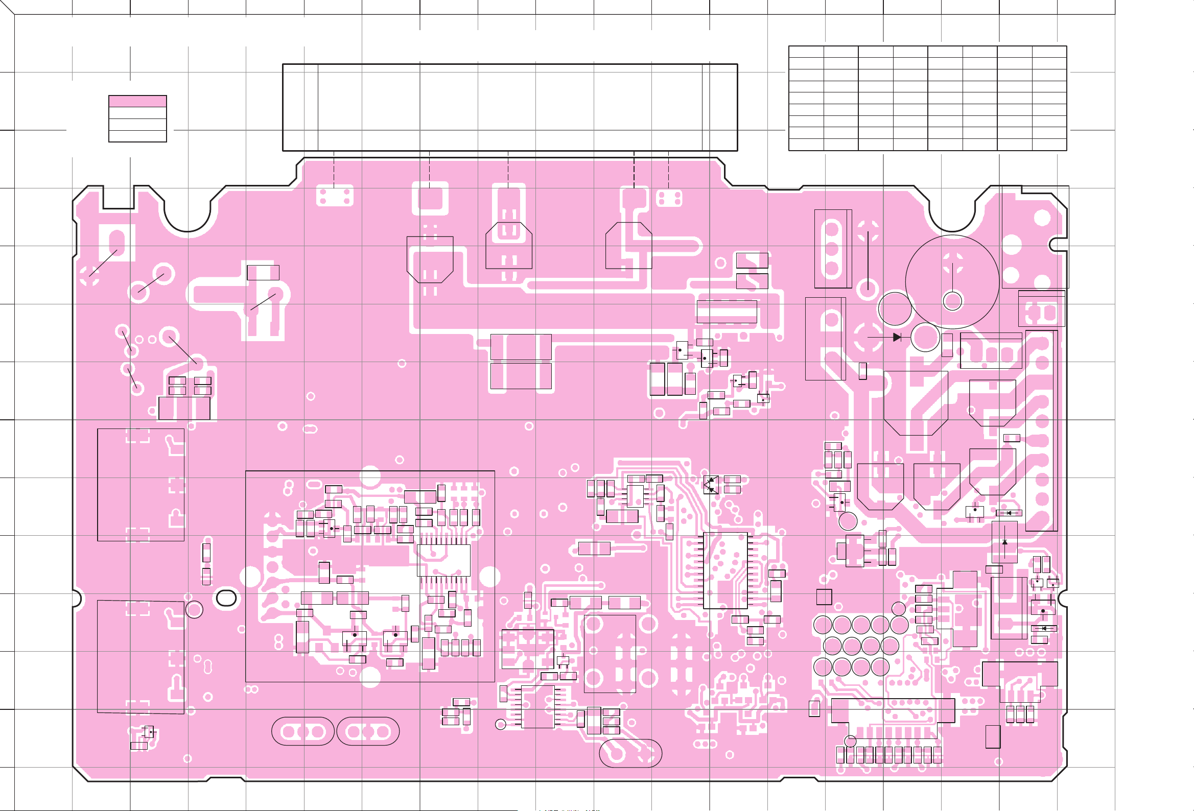
A
B
C
D E F G H
I J
K L M
N O
P Q R
S
TK-980/981 PC BOARD VIEW
1
Component side
2
Pattern 1
Pattern 2
Pattern 3
Pattern 4
Foil side
3
4
L224
5
L221
C273
L229
6
L222
L223
7
C128
C124
L220
C129
C125
R135
8
L203
A1
9
E
OUT
L8
10
C161
TP1
E
NC
8CL
MD
CV
11
L207
12
Q205
13
C171
J72-0816-09 A/2
51
14
5 4 3 2 1
R308
L303
C317
R309
R310
C321
Q300
C326
R319
+ +
C322
R318
+
C325
Q302
XF1
C320
C309
L304
R316
R317
TX-RX UNIT (X57-6520-XX) (A/2) -10 : TK-980 -11 : TK-981
Component side view
IC400
+
C259
C262
+
R255
R256
D
S
C100
Q32
+
C45
C96
R41
+ +
L5
+
C303
R320
R315
L300
R321
C307
C304
C327
R312
R311
L11
1011
C313
R306
+
C314
C306
IC300
R307
C315
C318
C94
C91
R303
R305
R313
R110
R301
R302
1
20
R118
R129
R322
TP3
L6
G
R121
C169
C102
89
IC11
1
16
C319
R314
R111
C308
C310
L301
Q301
C51
R45
CF1
C98
R119
C99
+
R42
C107
C41
+
C257
C43
1
IC6
4 5
X2
R120
R53
8
R55
R52
Ref No.
IC5 10M
IC6 9K
IC9 10O
IC10 8R
IC11 12J
IC14 6O
IC300 10H
IC400 2I
R89
R88
R127
Q20
C131
C115
Q13
Q21
R60
C54
R91
R47
C90
Q10
24
R57
C48
1312
C40
R48
R49
R113
R122
R99
R97
R98
D11
R171
1
IC5
Address
Q19
IC14
Q8
E
C3
C1
RSSI
E
C
B
O
G
I
R80
R77
R74
C63
OP
SQ2
C68
ST
C4 5C
SQ
C2
R4
Ref No.
Q4 11R
Q5 10R
Q6 10R
Q8 9O
Q9 9Q
Q10 7M
Q13 7M
Q19 5O
D32
+B
D37
C132
R76
C70
+
I
C71C65
G
O
IC9
RD2
TD2
RD1
FW TD1
CN1
8
ME/AM
PTT
SQ
MI/TXS
R3
C5C2C3
C6C9C7
Address
R70
E
DEO
DI
IGN
R2
Ref No.
Q20 6L
Q21 6L
Q32 12J
Q205 13C
Q300 9F
Q301 11G
Q302 11F
D7 11R
C152
+
R176
C79
+
C75
+
DTC/TXS/
FSW
MM
LOK/AM
DEO
3
1
1
C1
R8
C12
R7
R6
C11
C14
AHK/BUSY
R1
Address
3
SPI
CN5
Q9
CN2
Ref No.
D11 9M
D16 9R
D24 10R
D32 5O
D37 6P
J1
EXT. SP
CN6
1
PA
SPO
C77
+
R85
C74
+
D16
D24
C15
CN3
3
SB
E
1
HOR
CN4
3
RXD
TXD
C8
C13
E
Address
2
E
10
IC10
1
R50
R58
Q6
Q4
D7
C10
1
LOK
C4
1
SP
Q5
Page 52
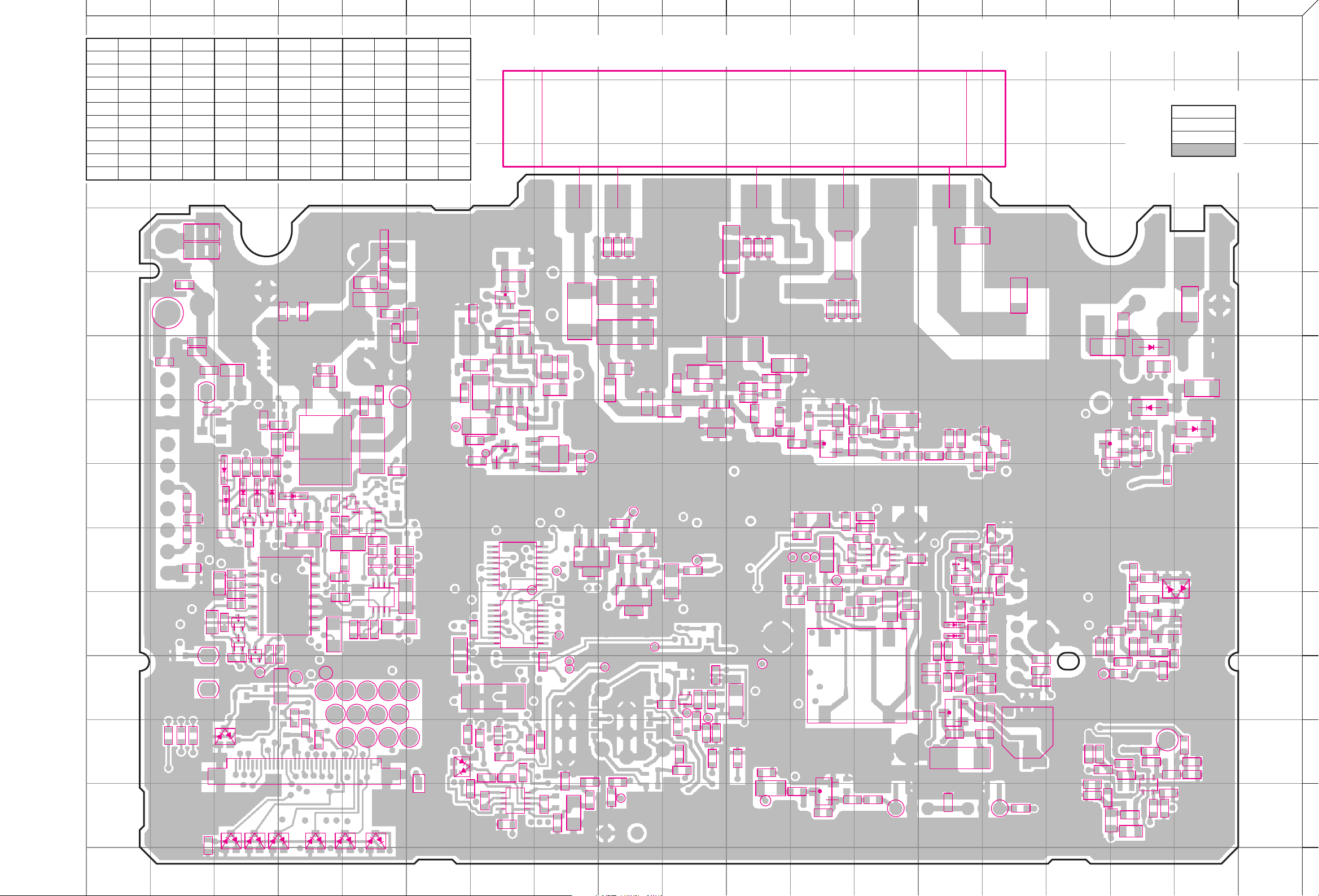
A
CB
D
E
IHGF
J
NMLK
O
RQP
S
Ref. No. Address
IC1 9M
IC2 13G
IC3 10E
IC4 8E
IC7 9G
IC8 10G
IC12 9H
IC13 6G
IC15 10D
IC16 10I
Ref. No. Address
IC400 2K
Q1 8E
Q2 11N
Q7 10O
Q11 7G
Q12 7H
Q15 13L
Q17 5G
Q18 11J
Q22 10C
R181
R182
C195
SP
C197
C196
C198
C89
PA
R106
C76
R86
C73
C72
SB
HOR
R9
R10
R11
Ref. No. Address
Q25 10C
Q26 10C
Q27 7D
Q28 8D
Q30 8C
Q31 8C
Q33 9N
Q34 7Q
Q201 10Q
Q202 7L
R109
C80
R152
R128
R144
R137
R145
R140
R141
Q22
R132
1
D2
R151
D34
D31
R154
Q30
R155
1
Q25
7
Q26
PSW
TO
NC
T/R
MO
W/N
PSW
BEEP
D3
D21
D20
R116
C136
C134
D6
Ref. No. Address
Q203 13Q
Q204 7J
D1 13D
D2 13C
D3 13C
D4 13C
D5 13E
D6 12C
D17 13E
D18 10N
C151
C438
R150
R143
IC15
ME
R134
C177
+
R153
MI
D26
AHK
C142
C162
LOK
IGN
R12
SB
SB
CN7
14
E
Q28
C127
8
R94
8C
KEY
R90
R156
D28
Q31
C123
MM
AFO
DEO
D4
D1
+
CK
C143
R148
E
R168
DT
RSSI
LD
Q27
C
R408
C24
ES
Ref. No. Address
D19 10N
D20 8C
D21 8C
D26 8D
D28 8C
D31 8C
D34 8C
D35 12F
D200 9R
D208 6Q
R102
+
C105
C106
C144
C137
B
R146
Q1
G
D
S
R17R39
3
4
IC4
1
5
R36
R411
+
C29
R20 R14
R23
R33
C19
8
1
+
C28
R30
C31
EP
EN
D17
R44
RD1TD2
FWTD1
E
CP
OE
DTC
TXD
RXD
FSW
APTT
D5
Ref. No. Address
D209 7Q
D210 7R
C109
C85 C97
C121
+
C126
SB
R414
C22
R21
+
5
C18
IC3
4
+
C36
C3C45CRD2DEO
OPSQ
C1C2
33
TX-RX UNIT (X57-6520-XX) (A/2) -10 : TK-980 -11 : TK-981
PC BOARD VIEW TK-980/981
1
Foil side view
Component side
IC400
Pattern 1
Pattern 2
Pattern 3
Pattern 4
1
R101
Q17
C150
R92
R112
C112
R105
TR
C110
8R
C78
C61
+
C46
C42
R73
R72
D35
RSSI
R31 R22
R32
C167
C87
4
5
C111
9
16
9
16
R71
R64
R19
R93
1
C83
R95
IC13
8
R103
R104
Q12
B
C
Q11
E
8
IC12
IC7
IC8
+
1
IC2
4
DT
1
ES
8
CK
1
BPO
R37
BP
R65
R63
R157
8
5
C21
+
R25
C23
C20
C284
R247
C255
R258
8T
C88
C117
I
O
G
IC16
DEO
C160 R163
R15
2
R248
R249
C166
C258
+
C172
I
DM
C256
5C
C116
G
C173
O
W/N
R166
C235
D18
D19
C66
C64
R75
Q33
5
R235
R231
C67
C158
L9
Q2
R40
C34
C84
C57
R67
C58
R226
C60
C159
C265
R69
Foil side
ANT
C266
C268
D208
C267
TH1
D209
TP1
C221
C220
R219
R218
Q34
C179
C227
C229
C214
C228
R211
R254
C216
R217
L210
L209
C219
L211
C209
L208
R210
C222
C176C178
C210
C211
R212
R139
C213
Q203
R209
C224
2 3
R172
L205
4
1
R214
C236
C240
C234
R223
R62
C56
R61
R66
C55
C175
Q7
L3
C62
R82
R79
R83
C33
+
E
R87
OUT
E
NC
C59
8CL
C170
L4
C39
C164
IN
MD
CV
C49
C47
R56
C37
+
R96
3
2
R253
TP2
L206
C218
C269
C271
D210
C272
C207
D200
4
1
Q201
C212
R220
R221
C215
C217
3
C261
C285
C328
R240
C114
+
C157
R250
R245
LD
C168
TP3
C252
R239
L10
C260
+
C251
R244
C276
C249
C38
R54
CP
DT
R28
R29
C153
L305
R252
+
C275
C274
L226
C253
C330
R159
+
C174
S
KEY
C108
R158
C118
R170
Q18
G
D
S
D
G
Q204
8C
C113
R124
C104
QAD
R251
C156
C155
C103
EP
L218
+
Q202
+
C25
C27
Q15
R107
4
L225
C264
C263
C286
+
R27
R100
C246
R323
C245
R241
R243
4
5
IC1
R160
1
8
R26
C32
L1
C52
OUT
R257
C247
R236
R237
C44
R46
R78
C35
+
R16
C16
C289
MB
R34
C30
X1
C92
2
3
4
5
6
7
8
9
10
11
12
13
C437
J72-0816-09 A/2
54
14
Page 53
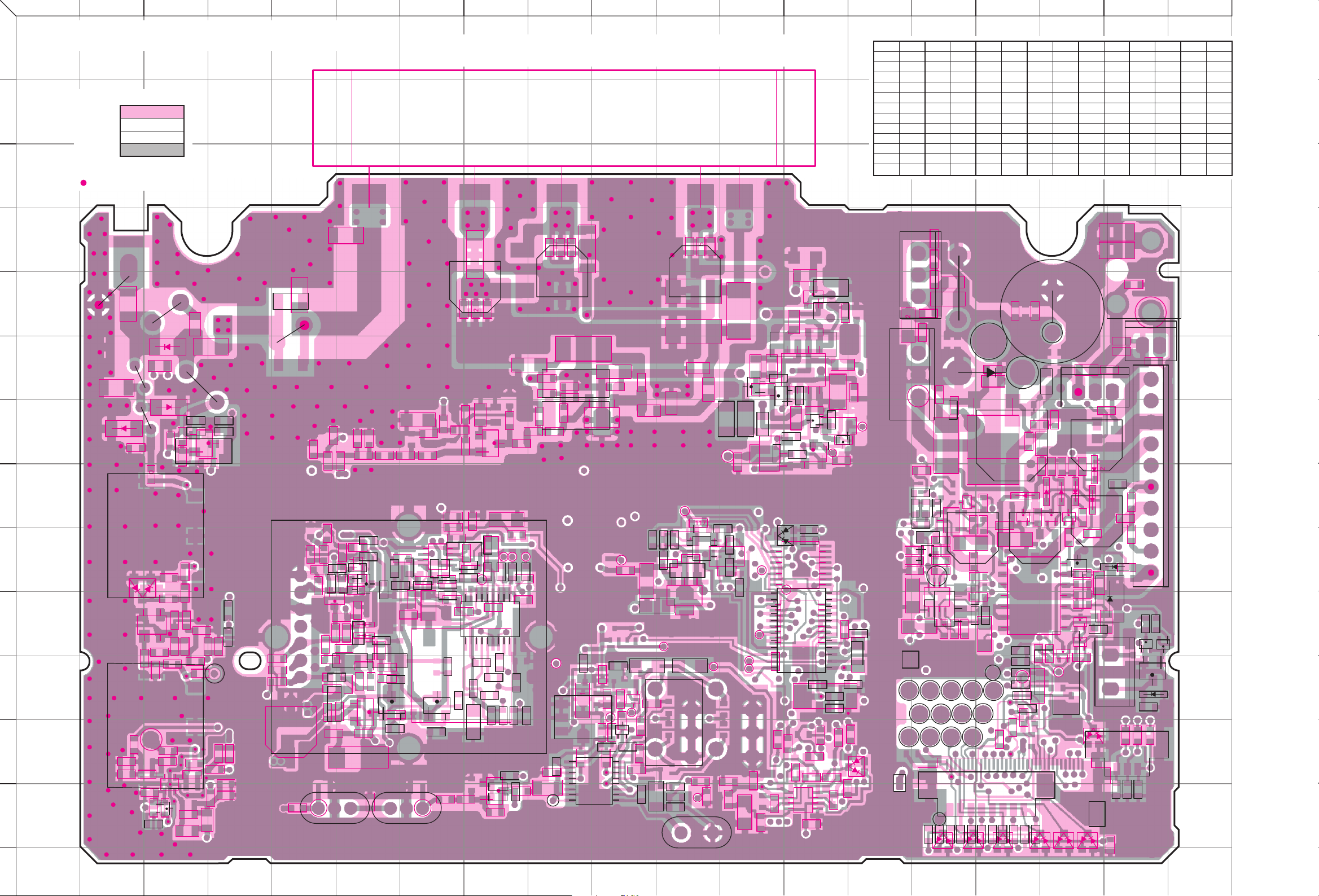
A
B
C
D E F G H
I J
K L M
N O
P Q R
S
TK-980/981 PC BOARD VIEW
1
Component side
2
Pattern 1
Pattern 2
Pattern 3
Pattern 4
Foil side
3
Connect 1 and 4
4
ANT
L224
5
6
C271
D210
7
L222
C269
C272
L221
TH1
L223
C207
D208
D209
C268
C267
L220
C128
C129
C125
C124
C176C178
R172
C179
Q34
R135
L229
C273
C266
C240
8
C49
C47
R56
A1
R66
C55
E
R87
OUT
Q7
E
NC
8CL
L4
MD
R82
CV
R83
C164
C37
+
IN
R96
10
11
12
13
L203
9
C209
C210
R221
C215
D200
4
1
Q201
L205
C212
L207
TP2
R220
L206
C218
C171
C217
C211
3
2
R253
R139
C213
Q205
R212
4
1
R214
R209
C224
2 3
C219
L211
L208
R210
C222
R211
C216
L209
Q203
C227
R254
C228
TP1
R218
L210
R217
C229
C214
C221
C220
L8
C161
R219
J72-0816-09 A/2
55
14
5
C265
C236
R223
R62
R61
C175
R309
C321
L3
C59
C170
+ +
R318
+
C325
C33
+
C234
R69
C322
C158
C56
R310
C57
C317
C62
R79
C39
R231
Q300
R40
C34
R226
R308
L303
Q33
C60
C326
C159
Q2
XF1
R235
R67
C58
C67
C235
D18
D19
R319
L9
L304
R75
C320
C66
C64
Q302
C84
C309
R316
R166
R317
TX-RX UNIT (X57-6520-XX) (A/2) -10 : TK-980 -11 : TK-981
Component side view + Foil side
IC400
C116
C51
R45
CF1
C98
R119
C99
C253
+
O
R42
C107
R248
R249
5C
C172
C41
C255
C117
+
G
DM
+
C256
C257
C43
1
IC6
4 5
X2
2
C258
C284
Q20
R258
R120
8T
R53
8
R55
O
G
R52
I
IC16
DEO
C160R163
C166
R15
R241
R160
C310
C52
C246
C308
C32
R243
R26
L301
OUT
+
C245
Q301
4
IC1
1
L1
R315
5
8
L300
R321
C307
R34
R100
R323
C44
R78
C327
C35
+
R27
R312
R236
C30
X1
C303
C304
C289
L11
MB
R311
C92
C264
C247
R237
1011
4
L225
C262
+
C263
R46
R16
C313
R306
+
C314
R257
Q202
R307
C315
Q15
R107
C286
R320
C306
C25
C27
+
IC300
C318
C94
C91
+
C16
C38
EP
R303
+
R305
R110
3
L305
C261
C285
C260
+
C259
R252
+
C276
R255
C252
C328
R239
R240
R256
R250
C251
L218
R54
DT
R313
C249
R302
R28
R29
1
20
R322
C319
R111
R244
CP
C168
C153
R245
R301
LD
R129
C114
R314
L10
TP3
+
L6
C157
C102
IC11
16
G
QAD
C275
S
C113
C155
R121
C103
C274
R118
R124
89
1
D
8C
R170
C156
+
Q204
C104
R251
D
G
C169
G
S
C118
C100
Q18
D
KEY
Q32
L226
C330
R41
C173
+
C174
+
C45
W/N
+ +
S
R159
C108
R158
L5
C96
1
R247
C88
I
R171
BPO
Ref. No. Address
IC1 9G
IC2 13M
IC3 10O
IC4 8O
IC5 10M
IC6 9K
IC7 9M
IC8 10M
IC9 10O
IC10 8R
IC11 12J
IC12 9L
R101
R89
Q17
R88
C87
R93
R127
1
C83
R95
Q21
B
C
E
R25
D11
1
R65
8
1
8
1
R99
8
R97
ES
R63
IC7
IC8
IC5
8
5
R104
R157
IC2
C115
C54
+
IC13
C111
Q13
Q11
R60
C42
R19
R91
9
16
9
16
R47
R64
1
4
C131
R103
R113
R122
R98
Q12
IC12
DT
CK
R37
BP
C21
+
C23
C20
C150
4
R92
5
R112
C112
C90
R105
TR
C110
Q10
8R
C78
24
C61
R57
+
C48
1312
R71
R31R22
R48
R49
C46
C40
R73
R72
D35
R32
C167
IC14
RSSI
Q19
E
C
B
C106
C121
+
O
G
I
SB
R414
R80
R77
R74
C63
C22
Q8
R21
+
C18
+
C36
E
C3
OP
C1
SQ2
Ref. No. Address
IC13 6M
IC14 6O
IC15 10P
IC16 10K
IC300 10H
IC400 2I
Q1 8O
Q2 11F
Q4 11R
Q5 10R
Q6 10R
Q7 10E
C109
C97
C85
C126
C68
5
4
C4 5C
C2
R4
C105
R76
R411
R20R14
R23
C19
ST
SQ
33
R102
C144
IC3
8
C9
D32
+
C137
C132
R146
Q1
D
3
4
IC4
1
5
+
C29
IC9
8
I
1
G
O
R30
R44
RD2
RD1
FW TD1
E
OE
TXD
RXD
FSW
PTT
SQ
R3
C7
D5
Ref. No. Address
Q8 9O
Q9 9Q
Q10 7M
Q11 7M
Q12 7L
Q13 7M
Q15 13H
Q17 5M
Q18 11J
Q19 5O
Q20 6L
Q21 6L
+B
C143
D37
R148
B
Q27
C
G
S
R17R39
C127
R36
C70
+
R33
R408
C24
C71C65
R70
+
C28
C31
E
DEO
TD2
EP
CP
ES
LD
EN
DTC
APTT
CN1
ME/AM
DI
MI/TXS
C6
C5C2C3
R2
D17
RSSI
+
LOK
R168
DT
IGN
C162
14
8
CK
CN7
Ref. No. Address
Q22 10Q
Q25 10Q
Q26 10Q
Q27 7P
Q28 8P
Q30 8Q
Q31 8Q
Q32 12J
Q33 9F
Q34 7C
Q201 10C
Q202 7H
C438
E
R90
C142
C79
+
D26
Q28
+
IC15
R8
C12
DTC/TXS/FSW
R7
MM
LOK/AM
R6
C177
C11
C14
R12
R94
MI
8C
SB
SB
IGN
KEY
AHK
AHK/BUSY
DEO
R1
D1
Ref. No. Address
Q203 13C
Q204 7J
Q205 13C
Q300 9F
Q301 11G
Q302 11F
D1 13P
D2 13Q
D3 13Q
D4 13Q
D5 13O
D6 12Q
C152
C151
+
R109
3
R176
SPI
CN5
C80
R150
R152
R143
R153
C75
R134
+
ME
MM
AFO
1
D4
C1
R128
R151
R156
D31
D34
D28
R154
R116
Q30
Q31
R155
1
7
3
C123
PSW
1
DEO
PSW
Q9
R144
R137
R145
R140
Q25
C15
Q26
Q22
R132
CN2
TO
NC
T/R
MO
W/N
1
BEEP
E
D3
D2
C89
SPO
R106
C77
+
D21
D20
C74
+
C136
R141
CN3
SB
HOR
R181
R182
D16
E
D6
3
C197
C196
1
PA
R85
R86
D24
C134
3
1
CN4
TXD
C13
C437
Ref. No. Address
D7 11R
D11 9M
D16 9R
D17 13O
D18 10F
D19 10F
D20 8Q
D21 8Q
D24 10R
D26 8P
D28 8Q
D31 8Q
J1
EXT. SP
C195
SP
2
1
E
SP
C198
10
IC10
C76
C73
C72
1
R50
R58
Q6
Q4
D7
C10
R9
R11
R10
1
RXD
LOK
C4
C8
Ref. No. Address
D32 5O
D34 8Q
D35 12N
D37 6P
D200 9B
D208 6C
D209 7C
D210 7B
CN6
Q5
Page 54
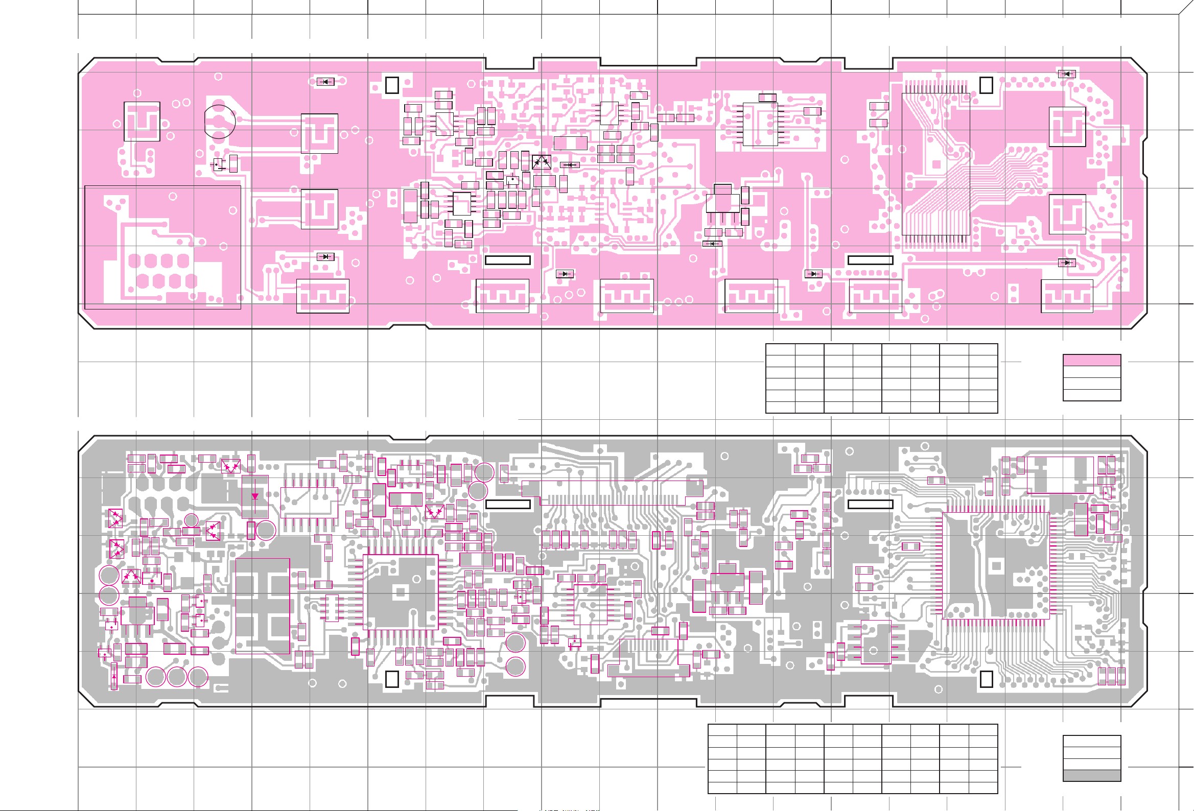
A
CB
D
E
IHGF
J
NMLK
O
RQP
S
TX-RX UNIT (X57-6520-XX) (B/2) -10 : TK-980 -11 : TK-981 Component side view
D512
C527
R526
445
IC501
8
C520
R532
+
C519
1
C506
R527
R528
C535
1
IC503
C523
R551
R569
C574
C505
C509
R502
R504
R503
R726
R554
C559
L503
Q5 03
R552
C547
8
R541
C540
R548
C542
R545
A
5
C553
C575
C564
R568
R553
C555
PSW
CM
HOOK/
RXD
J501
PTT/
MIC
TXD
ME E BLC
PSB
D511
Q511
R525
VOL
UP
C600
VOL
DN
D513
MON
C513
J72-0816-09 B/2
TX-RX UNIT (X57-6520-XX) (B/2) -10 : TK-980 -11 : TK-981 Foil side view
C510
D509
D514
D510
R573
PC BOARD VIEWS TK-980/981
D517
C518
1
8
IC502
4 5
R507
+
R508
C511
R523
C714
R530
R531
C561
C524
C522
R572
R612
D520
IC509
O
G
C593
C583
1
16
IC508
9
8
R587
I
C584
R682
D515
L507
C592
16
17
1
SYS
UP
IC510
SYS
DN
32
D516
1
2
3
4
5
B
C
D
SCN
6
Ref No.
Address
IC501 2G
IC502 2J
IC503 4G
IC508 2L
IC509 4L
Ref No.
Address
IC510 3O
Q503 3H
Q511 3C
D509 3I
D510 3I
Ref No.
Address
D511 2C
D512 2E
D513 5E
D514 5I
D515 5M
Ref No.
Address
D516 5R
D517 2R
D520 4K
Pattern 1
Pattern 2
Pattern 3
Pattern 4
Component side
7
Foil side
C501
R505
D505
R683
D507
Q513
B
R674
R680
C607
R701
C512
R512
C528
C
MPTT
D503
SPO
GND
C601
Q512
Q515
D518
J72-0816-09 B/2
L502
L501
E
R516
C726
R506
Q501
R679
R723
R724
R722
MUTE
C503
R513
C598
C599
GNDPTT
R668
R667
R702
D504
Q508
Q509
D501
C614
D502
C504
R725
X501
14
1
SB
C582
R579
C576
C577
8
R577
IC507
7
C578
R575
R544
C544
CP501
C536
R537
R538
C566
R566
R567
C554
22
23
33
34 44
R533
C525
3
C557
R721
C560
C558
IC504
4
C556
R524
IC711
C722
C517
C516
1
R719
R718
5
C715
+
D508
R555
12
11
1
R522
C514
C526
R521
R518
R520
C562
C563
C549
C569
R515
C728
C720
R519
C515
R571
TXAO
C572
R562
C550
+
C531
TXAI
C567
C548
R546
R540
R535
C521
C622
33
E
PSWOERXD
TXD
DTCCPAPTTENEPESLD
C624
C626
R556
C565
C628
R564
C545
R574
C571
C580
Q507
C723
R547
C546
C541
C529
R529
C537
C533
R536
R542
Q502
C539
C543
R550
C552
RXAI
RXAO
8
14
C570
IC506
CN502
RSSIDTCK
KEY8CSBSBIGN
AHKMIME
AFOMMDEO
PSW8RBEEPTOMO
C620
C617
C616
C632
R727
7
1
L508
R582
R558
C633
E
5C
CK
CS
NC
SID
1
CN501
1
T/R
W/N
C623
C625
R716
C627
C630
NC
NC
LEDK
LEDA
10
C579
R576
R580
C604
+
C602
C634
R673
C631
Ref No.
IC504 10F
IC506 11I
IC507 9D
IC511 10P
IC512 11N
IC513
O
R681
G
C609
C612
R678
I
Address
C613
+
Ref No.
IC513 10L
IC711 8F
Q501 10B
Q502 11H
Q507 11I
R720
C568
+
R670
R675
C608
C610
R616
R614
Address
R676
R677
C606
C581
R581
R672
C605
Ref No.
Q508 11C
Q509 11C
Q510 9R
Q512 11A
Q513 11B
R706
R705
5
IC512
8
Address
R658
4
1
Ref No.
Address
Q515 12A
D501 8C
D502 9D
D503 10A
D504 9C
R633
25
26
50
51
Ref No.
D505 9A
D507 10A
D508 9G
D518 12A
Address
L505
IC511
C594
R624
C595
Pattern 1
Pattern 2
Pattern 3
Pattern 4
X502
1
100
76
75
C717
+
Component side
Foil side
C603
R645
C596
L504
R585
R584
C597
Q510
L506
R586
R588
8
9
10
11
12
13
58
14
Page 55
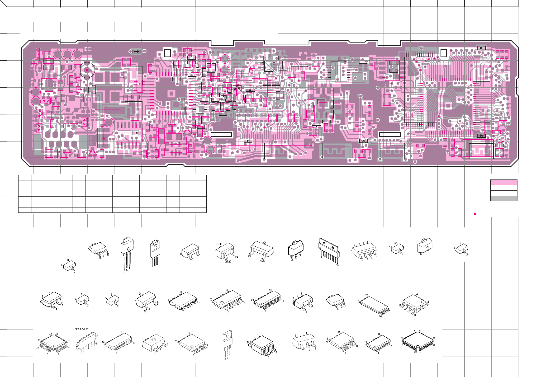
A
TK-980/981 PC BOARD VIEW
1
B
C
D E F G H
TX-RX UNIT (X57-6520-XX) (B/2) -10 : TK-980 -11 : TK-981 Component side view + Foil side
I J
K L M
N O
P Q R
S
2
C607
R683
R680
R674
PSW
B
Q513
D507
CM
HOOK/
RXD
R505
C501
MPTT
E
C
C528
R512
C512
L501
R701
MIC
ME E BLC
L502
R516
J501
PTT/
TXD
D518
Q515
3
Q512
C601
GND
4
SPO
D503
5
D505
6
J72-0816-09 B/2
Address
Ref No.
IC508 3M
IC509 4L
IC510 4P
IC511 4Q
IC512 3O
IC513 4L
7
IC501 3G
IC502 3J
IC503 4H
IC504 4G
IC506 4J
Ref No.
8
IC507 5E
Address
R722
R679
R724
Q501
R506
R723
C726
GNDPTT
R667
R668
C599
Q509
C598
Q508
C503
R513
D504
MUTE
PSB
R702
Ref No.
IC711 6G
Q501 4B
Q502 4I
Q503 4I
Q507 3J
Q508 4C
D511
Q511
R725
Address
C600
D502
D501
Ref No.
Q509 3C
Q510 5S
Q511 4C
Q512 3B
Q513 3B
Q515 3B
X501
C504
C614
SB
1
14
Address
D512
R538
R537
VOL
C536
UP
R544
C544
VOL
DN
C578
D513
IC507
MON
C582
Ref No.
D501 6D
D502 5D
D503 4B
D504 5C
D505 5B
D507 4B
C525
R533
34 44
33
CP501
23
22
R575
C554
R566
7
R567
C566
R577
8
C577
C576
R579
Address
Ref No.
D508 5G
D509 4I
D510 4J
D511 3C
D512 2E
D513 5E
+
C568
R720
R525
R524
C513
IC504
C556
C557
C558
C560
4
R721
3
Address
R520
C516
R518
C527
R521
R526
C514
C526
C517
IC501
8
C520
R532
+
R527
C519
R528
C523
12
R555
C562
C722
+
C715
5
1
IC711
R719
Ref No.
D514 5I
D515 5N
D516 5R
D517 2R
D518 2B
D520 5L
1
C506
11
D508
R718
C535
C549
R551
C563
C515
R515
R519
445
R522
1
R535
R503
C720
1
8
IC503
+
5
C550
R569
C574
C572
C569
C728
Address
C521
R504
C531
R540
R546
C548
C553
TXAO
R571
R726
C541
R562
TXAI
R529
C509
R536
R502
C529
C537
R552
C547
C540
R548
C567
C505
C533
R541
CN501
RXAO
RXAI
C580
C571
C552
R554
C559
R550
C539
C543
Q502
R542
Q50 3
R553
C542
R545
C546
R547
C723
C622
A
C510
L503
R574
D509
C545
C575
C565
C564
R568
C555
R556
C628
C626
E
OE
RXD
PSW
33
D514
Q507
R573
R564
C624
TXD
DTC
14
D510
8
C570
CP
APTT
+
IC506
C620
EP
EN
L508
IC502
R508
C511
ES
LD
RSSI
1
4 5
R507
1
7
R727
DT
CK
KEY
CN502
8
C617
8C
R523
C714
SB
SB
C518
1
R530
5C
CK
E
CS
R531
R558
R582
C561
C632
C616
MI
ME
IGN
AFO
AHK
B
10
C524
NC
LEDK
NC
LEDA
SID
C522
C633
C630
8R
TO
MM
DEO
PSW
BEEP
C631
R673
R572
NC
C634
C602
C609
+
C604
G
O
IC513
IC509
G
O
R580
R576
C627
T/R
MO
C579
C593
R612
R716
C625
D520
C623
W/N
1
C583
1
16
IC508
9
8
+
I
C613
R675
R587C584
I
R670
R678
R681
C612
C
R614
R616
C610
R682
D515
C608
C605
R581
C581
C606
R677
R676
L507
8
R672
C592
IC512
5
R705
R706
D
16
1
4
50
IC510
R658
17
26
R633
1
51
IC511
32
25
L505
R624
C594
C595
D517
SYS
UP
75
76
SYS
DN
100
D516
1
X502
SCN
Pattern 1
Pattern 2
Pattern 3
Pattern 4
R588
R585
R586
R584
+
L504
C603
C596
R645
L506
Q510
C597
C717
Component side
Foil side
Connect 1 and 4
10
11
12
13
14
9
DTA114EE
DTA144EUA
DTA144WE
DTC114EE
DTC144EE
DTD114EK
2SC3356
2SC3722K
2SC4116
2SC4226
2SC4617
2SC4619
2SB1132
2SC2873
2SA1362
2SC2059K
2SC2412K
2SC2712
3SK255
TC35453F
MA742
M67760HC
2SK508NV
M67760LC
2SA1641
2SB1370
2SC4094
DTC314TU
DTC363EU
4
2SK1824
3
E
C
B
TC4013BF
1
2
BU4066BCFV
SA7025DK RH5VL42C BU4094BCFV TA7808S
DTC144EUA
M62363FP
TA75W01FU
TC75W51FU
2SK2596
TC4S66F
TA75S01F
LA4422
NJM2904E
DAN202U
TA75W558FU
NJM78L08UA
AT29C020-90TI
W29C020C90
AT2408N10SI2.5
24LC08BT-ISN
TA31136FN LC73872M 30622M8A-4F9GP
TA78L05F
VREF
GND
VIN
DTA114YUA
HAM88AS
59
Page 56
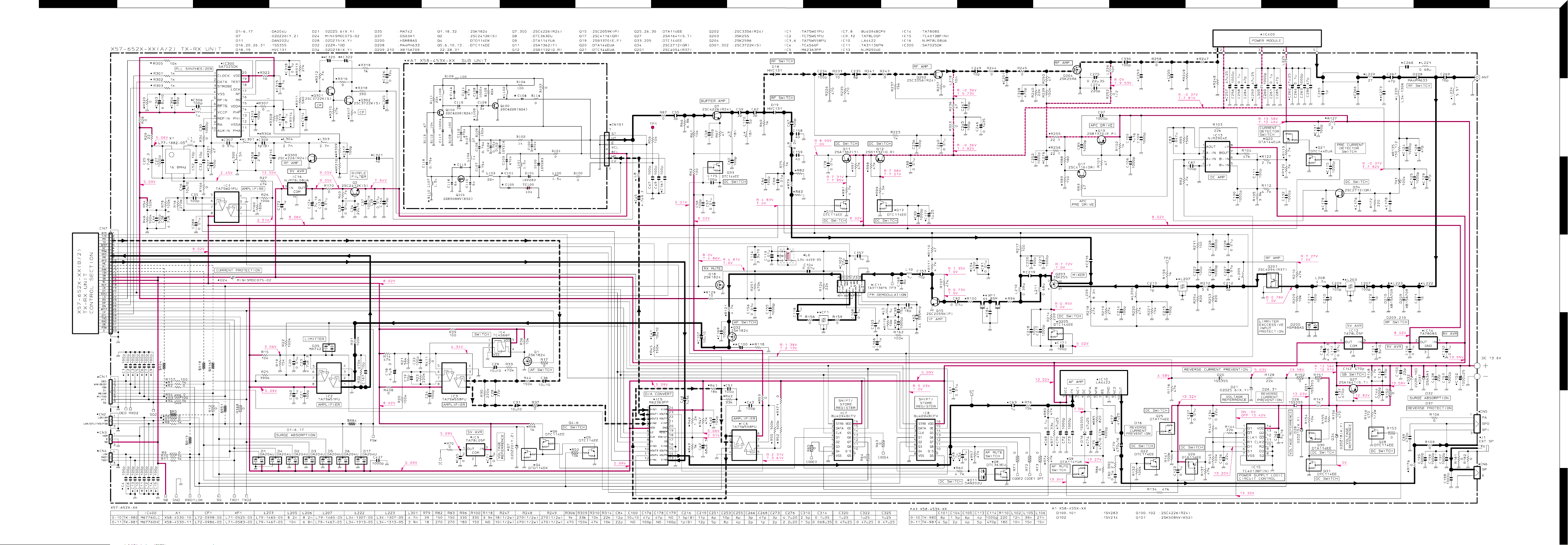
Note : Components marked with a dot (·) are parts of pattern 1.
OMKIGECA
SQ
TRPNLJHFDB
SCHEMATIC DIAGRAM TK-980/98 1
1
2
3
4
5
6
64
7
Page 57
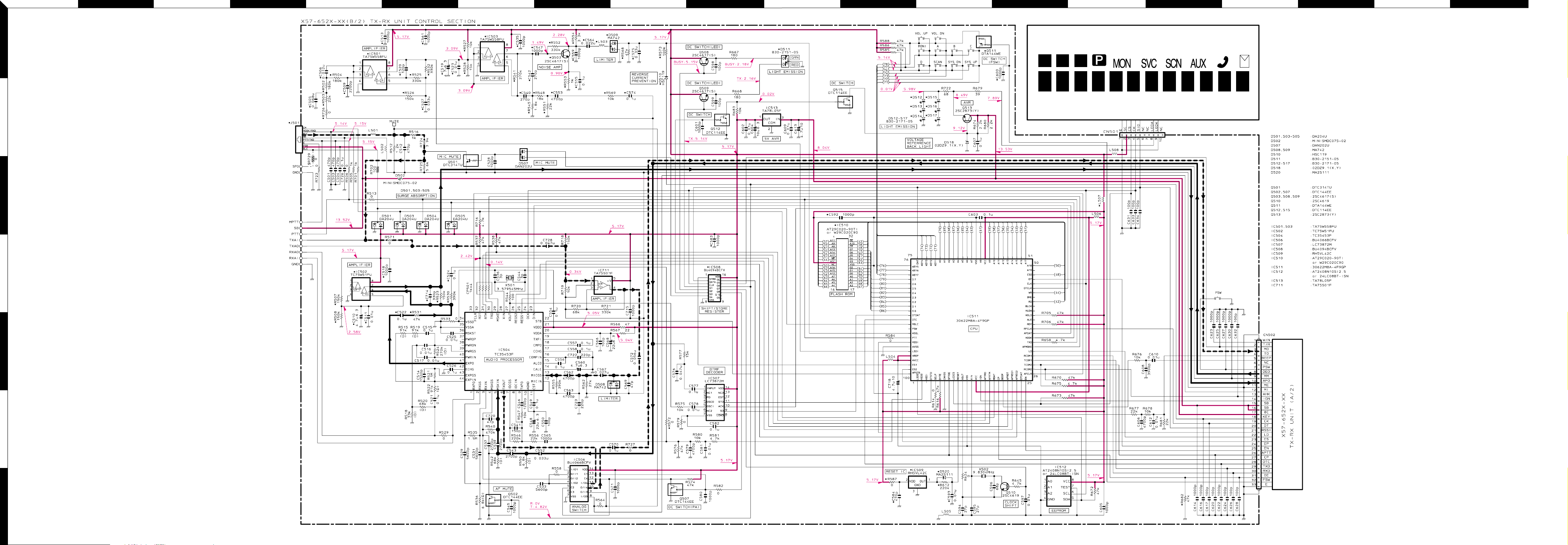
ACEGI K MOQS
BD
F H J L N P R T
TK-980/98 1 SCHEMATIC DIAGRAM
1
2
3
Note : Components marked with
a dot (·) are parts of pattern 1.
4
5
6
7
65
Page 58
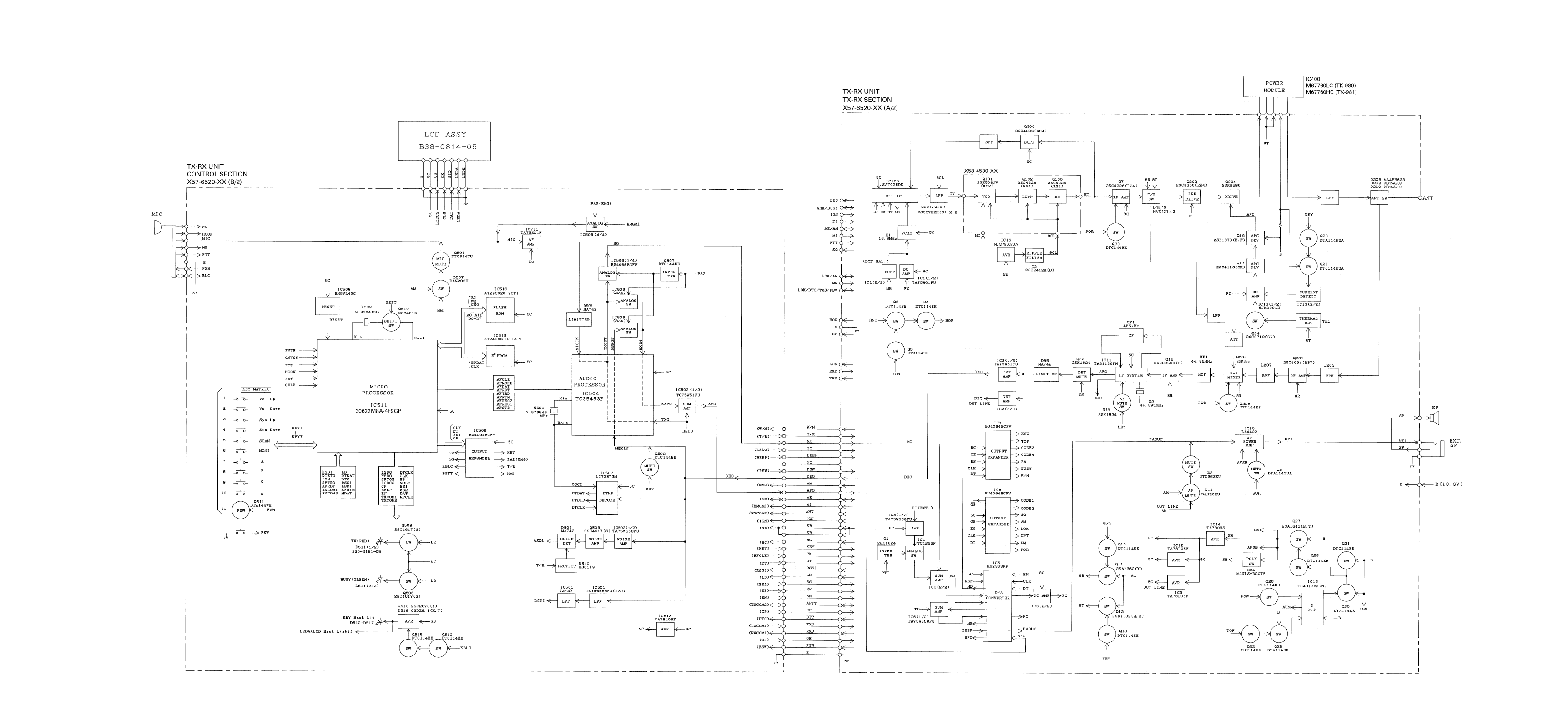
TK-980/981 TK-980/981 TK-980/981
BLOCK DIAGRAM
7069
71
Page 59
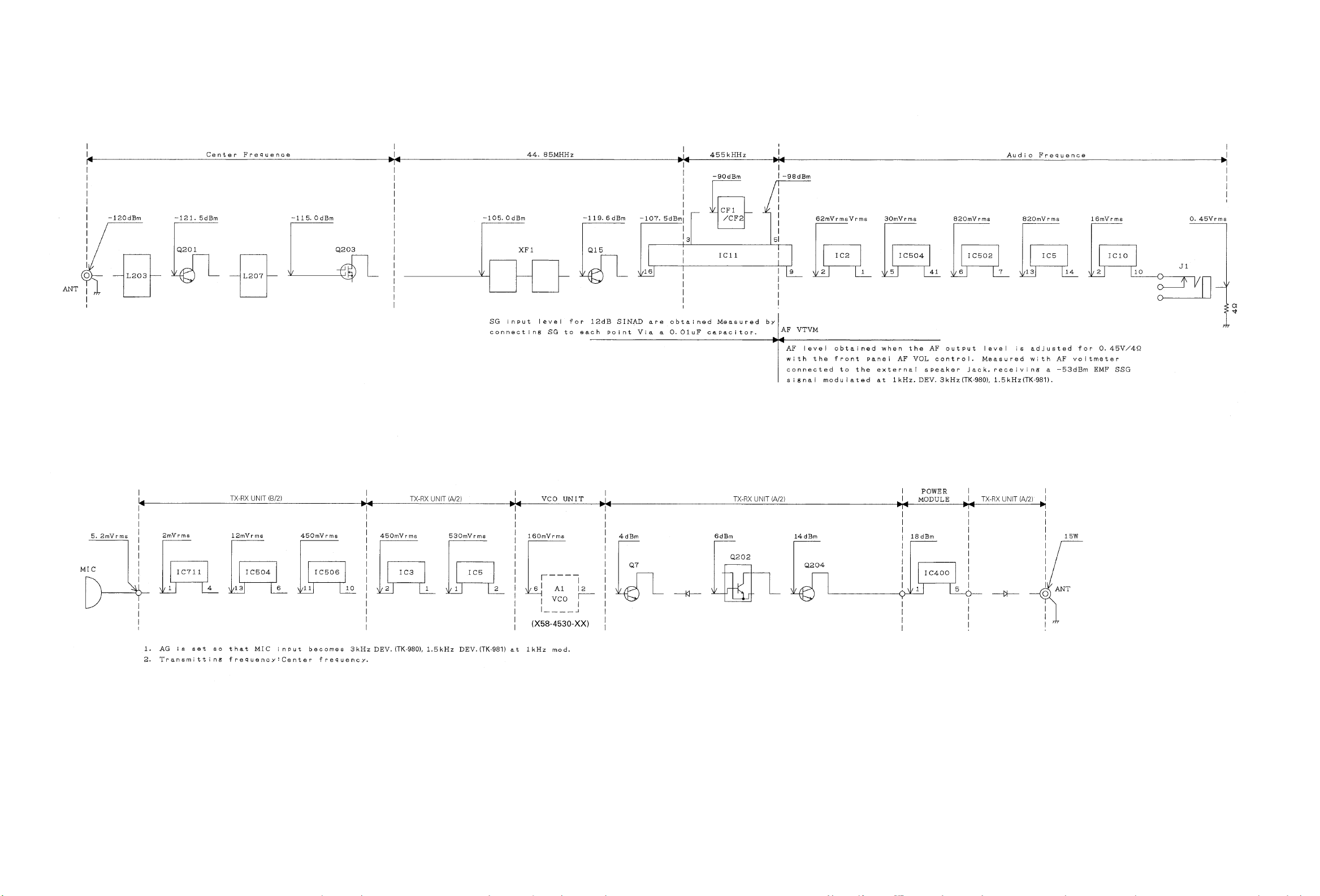
Receiver Section
TK-980 /98 1TK-980 /98 1
LEVEL DIAGRAM
Transmitter Section
7372
Page 60
TK-980/98 1
TERMINAL FUNCTION
CN7 (TX-RX Unit A/2) ←→ CN502 (TX-RX Unit B/2)
Pin No.
1 W/N Wide/Narrow switch input. H : Wide
2 T/R TX/RX switch input. H : Receive
3 MO Modulation signal input.
4 TO Low speed data signal input.
5 BEEP Beep input.
6 8R NC (8V)
7 PSW Power switch.
8 DEO Recovery signal output.
9 MM MIC mute. H : MIC mute
10 AFO Recovery signal input.
11 ME MIC ground.
12 MI Internal MIC output.
13 AHK Hook signal output. H : Off hook
14 IGN Ignition output.
15 SB 13.6V output.
16 SB 13.6V output.
17 8C 8V output.
18 KEY TX/Lock detection input.
19 CK Shift register clock input.
20 DT PLL/Shift register/DA converter input.
21 RSSI RSSI signal output.
22 LD PLL unlock detection output.
23 ES Shift register enable input.
24 EP PLL enable signal input.
25 EN DA converter enable signal input.
26 APTT PTT signal output.
27 CP PLL clock.
28 DTC Data control signal output.
29 TXD Serial data
30 RXD Serial data.
31 OE Serial data.
32 FSW Foot switch output.
33 E Ground.
Name Function
CN101 (VCO) ←→ TX-RX Unit (A/2)
Pin No.
1 E Ground.
2 HT Signal output.
3 E Ground.
4 NC Unused terminal.
5 8CL 8V input.
6 MD Modulation output.
7 CV Control voltage input.
Name Function
CN501 (TX-RX Unit B/2)
Pin No.
1 E Ground (0V).
2 5C Logic power.
3 CS Chip selector signal. L : Option
4 CK Serial clock signal.
5 SID Serial data input.
6 (NC) Unused terminal.
7 (NC) Unused terminal.
8 LED(A) LED anode terminal.
9 LED(K) LED cathode terminal.
10 NC Unused terminal.
Name Function
J501 (TX-RX Unit B/2)
Pin No.
1 BLC MIC backlight control.
2 PSB 13.6V.
3 E Ground.
4 PTT/TXD PTT.
5 ME MIC ground.
6 MIC MIC signal input.
7 HOOK/RXD Hook detection
8 CM MIC data detection.
Name Function
74
Page 61

TK-980/98 1
SPECIFICATIONS
GENERAL
Frequency Range ................................ TK-980 RX : 851~870MHz TX : 806~825MHz, 851~870MHz
TK-981 RX : 935~941MHz TX : 896~902MHz, 935~941MHz
Number of Channels ........................... Maximum 600 channels (LTR mode)
Maximum 250 channels (Conventional mode)
Channel Spacing ................................. TK-980 25kHz (PLL channel step 12.5kHz)
TK-981 12.5kHz (PLL channel step 12.5kHz)
Input Voltage ....................................... 13.6V DC negative ground
Current Drain ...................................... 0.4A on standby
1.0A on receive
7A on transmit
Temperature Range ............................ –30°C to +60°C (–22°F to +140°F)
Dimensions & Weight ........................ 140 (5.51) W x 40 (1.58) H x 145 (5.73) D mm (inch), 0.94kg (2.07 lbs)
RECEIVER (Measurements made per EIA standard EIA/TIA-603)
RF Input Impedance ........................... 50Ω
Sensitivity (EIA 12dB SINAD) ............. 0.25µV
Selectivity ........................................... TK-980 : 75dB TK-981 : 68dB
Intermodulation................................... TK-980 : 70dB TK-981 : 65dB
Spurious and Image Rejection............ 80dB
Audio Power Output ........................... 4W at 4Ω less than 5% distortion
Frequency Stability ............................. ±1.5ppm from –30°C to +60°C
Channel Frequency Spread ................ TK-980 : 19MHz TK-981 : 6MHz
TRANSMITTER (Measurements made per EIA standard EIA/TIA-603)
RF Power Output ................................ 15W
Spurious and Harmonics..................... –60dB
Modulation .......................................... TK-980 : 16K0F3E TK-981 : 11K0F3E
FM Noise ............................................ TK-980 : –45dB TK-981 : –40dB
Microphone Impedance...................... Low impedance
Audio Distortion .................................. TK-980 : 3% or less at 1kHz TK-981 : 5% or less at 1kHz
Frequency Stability ............................. ±1.5ppm from –30°C to +60°C
Channel Frequency Spread ................ TK-980 : 64MHz TK-981 : 45MHz
Specifications are for K (U.S.A) models only.
75
Page 62

TK-980/98 1
KENWOOD CORPORATION
14-6, Dogenzaka 1-chome, Shibuya-ku, Tokyo 150-8501, Japan
KENWOOD SERVICE CORPORATION
P.O. BOX 22745, 2201 East Dominguez Street, Long Beach, CA 90801-5745, U.S.A.
KENWOOD ELECTRONICS CANADA INC.
6070 Kestrel Road, Mississauga, Ontario, Canada L5T 1S8
KENWOOD ELECTRONICS DEUTSCHLAND GMBH
Rembrücker Str. 15, 63150 Heusenstamm, Germany
KENWOOD ELECTRONICS BELGIUM N.V.
Mechelsesteenweg 418 B-1930 Zaventem, Belgium
KENWOOD ELECTRONICS FRANCE S.A.
13, Boulevard Ney, 75018 Paris, France
KENWOOD ELECTRONICS U.K. LIMITED
KENWOOD House, Dwight Road, Watford, Herts., WD1 8EB United Kingdom
KENWOOD ELECTRONICS EUROPE B.V.
Amsterdamseweg 37, 1422 AC Uithoorn, The Netherlands
KENWOOD ELECTRONICS ITALIA S.p.A.
Via G. Sirtori, 7/9 20129 Milano, Italy
KENWOOD IBERICA S.A.
Bolivia, 239-08020 Barcelona, Spain
KENWOOD ELECTRONICS AUSTRALIA PTY. LTD.
(A.C.N. 001 499 074)
16 Giffnock Avenue, Centrecourt Estate, North Ryde, N.S.W. 2113 Australia
KENWOOD ELECTRONICS (HONG KONG) LTD.
Unit 3712-3724, Level 37, Tower one Metroplaza, 223 Hing Fong Road, Kwai Fong, N.T., Hong Kong
KENWOOD ELECTRONICS TECHNOLOGIES(S) PTE LTD.
Sales Marketing Division
1 Ang Mo Kio Street 63, Singapore 569110
 Loading...