


KENWOOD KDC-237SA, KDC-237SAY, KDC-237SG, KDC-237SGY Service Manual
CD RECEIVER
KDC-237SA/237SAY KDC-237SG/237SGY
SERVICE MANUAL
© 2006-12 PRINTED IN JAPAN B53-0481-00 (N) 345
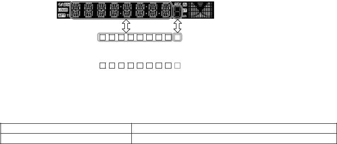
SPARE TDF PANEL
MAIN UNIT NAME |
TDF PARTS No. |
TDF NAME |
KDC-237SA/237SAY |
Y33-2660-62 |
TDF-237A |
KDC-237SG/237SGY |
Y33-2660-63 |
TDF-237G |
Panel assy
KDC-237SA/237SAY/237SG/237SGY (A64-4059-02)
B.BOOST
MENU

 /PTY
/PTY
DISP
KDC-237
FM
VOL |
SCRL |
AUD
 SET UP
AM
TI AME |
SCAN |
RDM |
REP |
ATT
Lever |
DC cord |
Carrying case |
(D10-4589-04) x2 |
(E30-6427-05) |
(W01-1685-05) |
Antenna adaptor |
Escutcheon |
Mounting hardware assy |
(T90-0523-05) |
(B07-3122-01) |
(J21-9716-03) |
This product uses Lead Free solder.

KDC-237SA/237SAY
KDC-237SG/237SGY
BLOCK DIAGRAM
ELECTRIC UNIT (X34- )
J2 |
ANT. |
|
|
|
|
Q901-903 |
|
|
|
|
|
|
|
|
|
||
A1 |
J4 |
BU |
DME1 |
|
|
DC-DET |
|
|
TUNER |
AM+B LX-BUS BU |
CD |
|
BU |
|
R103 |
|
|
FRONT-END |
A8V |
A8V |
MECHA |
|
IC6 |
PHONE |
PHONE |
BU5 |
SW5 |
SERVO+B |
|
||||||
|
|
|
|
|
||||
|
|
|
16 |
3 |
POWER |
|
Q101 |
|
3 |
|
|
IC |
|
|
|||
|
|
|
|
|
|
|
|
|
|
|
|
IC9 |
|
|
Q401 |
|
|
|
|
|
|
|
1 |
|
|
|
ACC DET |
ACC-DET |
|
|
|
|
|
|
|
ANALOG |
|
A8V |
SW |
A8V |
|
|
|
|
|
|
|
|
|
|
|
|||
|
|
|
|
|
|
|
|
|
|
|
|
|
|
|
|
Q103 |
|
||||||
|
|
|
|
|
|
|
|
1 |
|
|
|
|
|
|
|
|
|
|
|
||||
|
|
|
|
|
SW |
|
|
|
CONT |
|
|
|
|
|
|
|
|
|
|
BU DET |
BU-DET |
BU5 |
|
|
|
|
|
|
|
|
|
|
|
|
|
|
|
|
|
|
|
|
|
|
|||
|
|
|
|
IC2 or IC3 |
|
|
|
|
|
|
|
|
|
|
|
|
|
|
|
|
|||
|
|
|
|
|
|
|
|
|
|
|
|
|
|
|
|
|
|
|
|
Q102 |
|
||
|
|
|
|
|
|
|
|
|
|
|
|
|
1 |
|
|
|
Q701-704 |
CN4,J5 |
|
|
|
||
|
|
|
|
|
|
|
|
|
|
|
MUTE |
|
|
|
|
|
SURGE- |
|
|||||
|
|
|
|
|
|
|
|
E-VOL |
|
|
|
|
|
|
|
|
|||||||
|
|
SW5 |
|
|
|
|
|
|
|
|
|
|
|
|
|
PRE-OUT |
|
|
|||||
|
1 |
A8V |
|
|
|
|
|
|
|
|
|
|
PRE-OUT |
|
DET |
|
|||||||
|
|
|
|
|
|
|
|
|
|
|
|
|
|
|
|||||||||
IC7 |
|
|
|
|
|
|
|
|
|
|
|
|
|
FRONT/ |
|
|
|
|
|||||
|
|
|
|
|
|
|
|
|
|
|
|
|
|
|
MUTE |
|
|
|
|
||||
|
|
|
ROM CORRECTION (NOT USED) |
|
|
|
|
|
|
|
|
REAR/SW |
|
|
|
|
|||||||
|
RDS |
|
|
|
|
|
|
|
|
|
|
|
|
|
|
||||||||
|
|
|
|
|
|
|
|
|
|
|
|
|
|
|
IC4 |
|
|||||||
|
DECODER |
|
|
IC10 |
|
|
|
|
|
|
|
|
|
|
|
|
|
|
|
|
|
||
|
|
|
|
|
|
|
|
|
|
|
|
|
|
BU5 |
|
|
|
|
|
|
|||
|
|
|
SW5 |
E2PROM |
|
|
|
|
|
|
|
|
|
|
|
PS1-1 / PS1-2 / PS1-3 |
|
|
|||||
|
|
|
|
2 |
|
1 |
1 |
|
|
|
|
|
BU5 |
|
|
|
|||||||
3 |
3 |
|
8 |
|
|
|
|
|
|
|
|
|
|
|
|
|
|||||||
IC1 |
|
|
|
|
|
|
|
|
|
|
|
|
|
|
|
|
Q705 |
|
PS2-1 / PS2-2 |
|
|
||
|
|
|
|
|
|
|
|
|
|
|
|
|
|
|
|
|
|
|
|
|
|
||
|
|
|
|
|
|
|
|
|
|
|
|
|
|
|
BU5 |
MUTE |
BU DET |
|
FL+B |
|
|
||
|
|
|
|
|
|
|
|
|
|
|
|
|
|
|
|
|
RST |
|
|
AM+B |
|
|
|
|
|
|
|
|
|
|
|
|
|
|
|
|
|
|
|
|
|
|
|
|
|
||
|
|
|
|
|
SYSTEM u-COM |
|
|
|
|
|
|
9 |
|
|
|
|
|
SW5 |
POWER |
|
|||
|
|
|
|
|
|
|
|
|
|
|
|
1 |
|
|
|
SUPPLY |
|
||||||
|
|
|
|
|
|
|
|
|
|
|
|
|
|
|
|
|
|
|
|
|
|
||
|
|
|
|
|
|
|
|
|
|
|
|
|
|
|
|
|
|
|
|
|
A8V |
IC |
|
|
|
|
|
|
|
|
|
|
|
|
|
|
|
|
|
|
|
|
|
|
|
|
|
|
|
|
|
|
|
|
|
|
|
|
|
|
|
|
|
|
DC-CN etc |
|
|
|
SW5 |
|
|
|
IC8 |
|
1 |
1 |
2 |
1 |
|
1 |
5 |
|
|
|
|
|
|
|
|
|
|
D5 |
|
|
|
|
|
|
|
|
|
|
|
|
|
PHONE |
|
|
|
|
|
||||||||
|
|
|
|
|
|
|
|
|
|
|
|
|
BU5 |
|
|
||||||||
BU5 |
RESET IC |
|
|
|
|
Q301 |
|
|
|
|
|
|
|
ACC DET / BU DET |
|
|
|
|
|||||
|
|
|
|
|
|
|
|
|
|
|
P.ON FL |
|
|
|
|
|
|
||||||
|
WIRED |
|
|
|
|
SW5 |
BU5 |
|
ILLUMI+B |
R11-15 |
|
|
|
|
PS1-1 / PS1-2 / PS1-3 |
|
SERVO+B |
CD |
|
||||
|
|
|
|
|
|
|
|
|
|
|
PS2-1 / PS2-2 |
|
|
||||||||||
|
CN3 |
|
|
|
|
|
|
PAN5V |
|
|
1/2W |
|
|
|
1 |
|
|
|
Q2 |
|
|||
|
|
|
|
|
|
|
|
|
|
|
FL+B |
|
|
|
|
|
|
|
|||||
|
|
|
|
|
|
|
|
|
|
|
Rx5 |
|
|
|
|
|
|
|
|||||
|
|
|
|
|
|
|
|
|
|
|
|
|
|
|
Q302 |
|
|
|
|
|
|
||
|
REMOTE |
|
|
|
|
|
|
|
|
|
|
|
|
|
DSI |
BU5 |
|
|
|
|
SERVO |
|
|
|
|
|
J3 |
|
|
|
|
|
|
|
|
|
|
|
|
|
|
|
|
|
|
Q1 |
|
|
|
|
CN |
|
|
|
|
|
|
|
|
|
|
|
|
|
|
|
|
|
|
||
|
|
|
|
|
|
|
|
|
|
|
|
|
|
|
|
|
|
|
|
SW14V |
SW5 |
||
to GND |
|
J1 |
|
|
|
|
|
|
|
|
|
|
R80-82 |
|
|
|
|
|
|
|
|||
|
|
|
|
|
|
|
|
|
|
|
|
|
|
|
|
|
|
|
|||||
|
|
|
|
|
|
|
|
|
|
|
|
1/2W |
FL+B |
|
|
|
|
|
|
Q8,9 |
|
||
PANEL DET |
|
|
|
|
|
|
|
|
|
|
|
|
|
|
|
|
|
|
|||||
|
|
|
|
|
|
|
|
|
|
|
Rx3 |
|
|
|
|
|
|
|
ILLUMI |
|
|||
|
|
|
|
|
|
|
|
|
|
|
|
|
|
|
|
|
|
|
ILLUMI+B |
|
|||
|
|
|
|
|
|
|
|
|
IC1 |
|
|
|
|
ED1 |
|
|
|
|
+B |
|
|||
|
|
|
|
|
|
|
|
|
|
|
|
|
|
|
|
|
|
|
|
||||
S3 |
|
J2 |
|
S1 |
|
|
|
|
|
|
|
|
|
|
|
VFD |
|
|
|
|
|
Q7 |
|
RESET |
F-AUX |
ROTARY |
|
|
|
VFD |
|
|
|
|
|
|
|
|
|
|
SW14V |
P.ON FL |
|||||
|
|
|
|
|
|
|
|
|
|
|
|
|
|
||||||||||
ENCODER |
|
|
|
DRIVER |
|
|
|
|
|
|
|
|
|
|
|
||||||||
|
|
|
|
|
|
|
2 |
KEY |
|
|
|
|
|
|
|
|
|
|
|||||
|
|
|
|
SW5 |
|
|
|
|
|
|
|
|
|
|
|
|
|
|
|
|
|
||
|
|
|
|
|
|
|
|
|
|
|
|
ILLUMI |
|
|
|
|
|
|
|
|
|
||
|
|
|
|
|
|
|
|
|
|
|
|
|
|
|
|
|
|
|
|
|
|
||
|
|
IC2 |
SW5 |
|
|
|
|
9 |
|
|
|
KEY |
|
|
|
|
|
|
|
|
|
|
|
|
|
|
|
|
|
|
|
|
|
|
|
|
|
|
|
|
|
|
|
||||
|
|
REMOTE |
|
|
|
|
|
|
|
|
|
MATRIX |
|
|
|
|
|
|
|
|
|
||
SWITCH UNIT (X16- ) |
|
|
|
|
|
|
|
|
|
|
|
|
|
|
|
|
|
|
|
|
|||
|
|
|
|
|
|
CD PLAYER UNIT (X32-598x-xx) |
|
|
|
|
|
|
|
|
MOTHER |
|
|||||||
|
|
|
|
|
|
|
|
|
|
|
|
|
|
|
|
|
|
|
|
|
|
||
|
|
DPU1 |
|
|
|
|
|
|
|
IC1 |
|
|
|
|
|
|
|
|
BOARD (X34- ) |
|
|||
|
|
|
|
|
|
|
|
|
|
|
|
|
|
|
|
|
|
|
|
|
|
||
|
|
|
|
|
|
|
|
|
|
|
|
|
|
RST |
|
|
|
|
|
|
MRST |
|
|
|
|
|
|
|
|
|
|
D.GND |
A,B,C,E,F |
|
|
|
|
MSTOP |
|
|
|
|
|
|
MSTOP |
|
|
|
|
|
A |
B |
|
|
|
|
|
|
|
|
|
|
|
Q3 |
|
|
|
|
|
|
|
|
|
|
|
|
|
|
|
|
|
|
|
CLK |
|
|
LEVEL SHIFT |
|
CLK |
|
|
||||
|
|
|
E |
F |
|
|
|
|
|
|
|
|
|
LEVEL SHIFT Q3 |
|
|
|
||||||
|
|
|
|
|
|
|
|
|
|
|
|
|
|
|
|
|
|
|
|||||
|
|
|
C |
|
|
|
Q7 |
|
|
|
1 CHIP IC |
DATA |
|
|
|
DATA |
|
|
|||||
|
|
|
|
|
|
|
|
APC |
|
|
|
RF AMP |
|
|
|
|
Q4 |
LEVEL SHIFT |
|
|
|
|
|
|
|
|
|
|
|
|
|
|
|
|
|
+ |
|
|
|
|
|
MUTE |
|
||||
|
|
|
|
|
|
|
|
|
|
|
|
SERVO |
|
|
|
|
|
|
|
|
MUTE |
|
|
|
|
|
|
|
|
|
|
|
|
|
|
PROCESSOR |
|
|
|
(0-00),(0-01) ONLY |
|
||||||
|
|
|
|
|
|
|
|
|
|
|
|
|
|
|
|
|
|
||||||
|
|
|
|
|
|
|
|
|
|
|
|
+ |
|
|
|
|
|
|
|
||||
|
|
|
|
|
|
|
IC6 |
|
|
|
|
|
|
|
|
|
|
|
L-ch |
|
|
||
|
|
|
|
|
|
|
|
|
|
MICRO |
|
|
|
|
|
|
|
|
|
|
|||
|
|
|
|
|
|
|
|
|
|
|
|
|
|
|
|
|
|
|
|
R-ch |
|
|
|
|
|
|
FO COIL |
|
|
FO OUT |
|
|
|
PROCESSOR |
|
|
|
|
|
|
|
A.GND |
|
||||
|
|
|
|
|
|
|
|
|
|
|
|
|
|
|
|
|
|
|
|
|
|
||
|
|
|
TR COIL |
|
|
TR OUT |
|
|
|
|
|
AVDD |
IC3 |
3.3V REG |
8V SW |
Q1 |
|
AS8V |
|
|
|||
|
|
|
|
|
|
|
|
VREF |
|
|
VREF |
|
|
|
|
||||||||
|
|
|
|
|
|
|
|
|
|
|
|
|
|
|
|
|
|
|
|
|
|||
|
|
|
|
|
|
|
MOTOR |
FOD,TRD, |
|
|
|
|
|
|
|
Q8,9 SW |
Q2 |
(0-00),(0-01) |
|
|
|||
|
|
|
DM1 |
|
|
|
TVD,SPL |
|
|
|
|
|
|
|
SW |
ONLY |
|
|
|
||||
|
|
|
|
|
|
DRIVER |
|
|
|
|
|
|
|
|
|
|
|
|
|
|
|
||
|
|
|
SPINDLE |
|
|
DM OUT |
|
|
DMUTE |
|
|
|
|
|
|
|
|
D.GND |
|
||||
|
|
|
MOTOR |
|
|
|
|
|
|
|
|
|
|
D.GND |
|
|
|||||||
|
|
|
|
|
|
|
|
|
|
|
|
|
Q6 |
IC2 |
|
|
|||||||
|
|
|
|
|
|
|
|
|
|
|
|
|
|
|
|
|
|
|
|
|
|
||
|
|
|
DM2 |
|
|
|
|
|
|
|
|
|
|
IOVDD |
|
|
3.3V SW |
3.3V REG |
BU5V |
|
|||
|
|
|
LOADING & |
|
|
|
|
|
|
|
|
|
|
|
|
|
|
|
|
|
|
|
|
|
|
|
SLED |
|
|
|
FM OUT |
|
|
|
|
|
|
|
|
|
|
|
|
S7V |
|
|
|
|
|
|
MOTOR |
|
|
|
|
|
|
|
|
|
P-ON1 |
|
|
SW |
|
|
|
|
|
||
|
|
|
|
|
|
|
|
|
|
|
|
|
|
(0-01),(0-03) |
|
|
|
||||||
|
|
|
|
|
|
|
|
|
|
|
|
|
|
|
|
|
|
|
|||||
|
|
|
|
|
|
|
|
|
|
|
|
|
REGVDD |
|
|
|
ONLY |
|
|
|
|
||
|
|
|
|
|
|
|
|
|
|
|
|
|
|
|
|
|
|
|
|
|
|
||
|
|
|
|
|
|
|
|
S.GND |
|
|
|
|
|
|
|
|
|
|
S4 |
|
|
||
|
|
|
|
|
|
|
|
|
|
|
X1 or |
|
|
|
|
|
|
|
|
8EJE-SW |
|
||
|
|
|
|
|
|
|
|
|
|
|
|
D.GND |
|
|
|
|
|
|
|
|
|
||
|
|
|
|
|
|
|
|
|
|
|
X2 |
|
|
|
|
|
|
S3 |
|
|
|||
|
|
|
|
|
|
|
|
|
|
|
|
|
|
|
|
|
|
|
|
||||
|
|
|
|
|
|
|
|
|
|
|
|
CLOCK |
|
|
|
|
|
|
|
|
|
||
|
|
|
|
|
|
|
|
|
|
|
|
|
|
|
|
|
|
|
|
LOE/LIM-SW |
|
||
|
|
|
|
|
|
|
|
|
|
|
|
16.93MHz |
|
|
|
|
|
|
S2 |
|
|
||
|
|
|
|
|
|
|
|
|
|
|
|
|
|
|
|
|
|
|
|
|
|
||
|
|
|
|
|
|
|
|
|
|
|
|
|
|
|
|
|
|
|
|
|
12EJE-SW |
|
|
|
|
|
|
|
|
|
|
|
|
|
|
|
|
|
|
|
|
|
|
S1 |
|
|
|
|
|
|
|
|
|
|
|
|
|
|
|
|
|
|
|
|
|
|
|
|
LOS-SW |
|
|
|
|
|
|
|
|
|
|
|
|
|
|
|
|
|
|
|
|
D.GND |
|
S.GND |
|
||
|
|
|
|
|
|
|
|
|
|
|
|
|
|
|
|
|
|
S.GND |
|
|
|||
|
|
|
|
|
|
|
|
|
|
|
|
|
|
|
|
|
|
|
|
|
LO/EJ |
|
|
|
|
|
|
|
|
|
|
|
|
|
|
|
|
|
|
|
|
|
|
|
MOTOR |
|
|
J1
DC-CN
PHONE
SP-OUT
ACC
B.U.
P-ANT P-CON
2
KDC-237SA/237SAY
KDC-237SG/237SGY
COMPONENTS DESCRIPTION
● ELECTRIC UNIT (X34-4672-78)
Ref. No. |
Application / Function |
Operation / Condition / Compatibility |
|
|
|
IC1 |
System -COM |
Controls FM/AM tuner, the changer, CD mechanism, panel, volume and tone. |
|
|
|
IC3 |
E-VOL |
Controls the source, volume and tone. |
|
|
|
IC4 |
Power Supply IC |
Outputs 5Vx2, 8.1Vx2, 10.2V, P-CON and P-ANT. |
|
|
|
IC6 |
Power IC |
Amplifies the front L/R and the rear L/R to 45W maximum. |
|
|
|
IC7 |
RDS IC |
RDS decoder. |
|
|
|
IC8 |
Reset IC |
Lo when detection voltage goes below 3.6V. |
|
|
|
Q1 |
SW14V |
ON when the base goes Hi. |
|
|
|
Q2 |
Servo+B AVR |
When Q3’s base goes Hi, Servo+B AVR outputs 7.5V. |
|
|
|
Q3 |
Control SW for Servo+B |
ON when the base goes Hi. |
|
|
|
Q7 |
VFD+B SW |
ON when the base goes Hi. |
|
|
|
Q8 |
VFD+B AVR |
When Q9’s base goes Hi, Servo+B AVR outputs 10.5V. |
|
|
|
Q9 |
Control SW for VFD+B |
ON when the base goes Hi. |
|
|
|
Q101 |
ACC DET |
ON when the base goes Hi during ACC is applied. |
|
|
|
Q102 |
Serge DET |
When the base goes Hi, surge voltage is detected. |
|
|
|
Q103 |
BU DET |
ON when the base goes Hi during BU is applied. |
|
|
|
Q104,105 |
Mute Control |
ON when the base goes Hi. |
|
|
|
Q301 |
Panel 5V SW |
ON when the base goes Lo. |
|
|
|
Q302 |
DSI ILLUMI SW |
ON when the base goes Hi. |
|
|
|
Q901 |
DC Offset DET |
ON when the base goes Hi after Q902’s and Q903’s outputs are separated. |
|
|
|
Q902,903 |
DC Offset DET SW |
ON when the bases go Lo after IC6’s SP-OUTs (DC) are separated. |
|
|
|
● SWITCH UNIT (X16-386x-xx)
Ref. No. |
Application / Function |
Operation / Condition / Compatibility |
|
|
|
IC1 |
VFD Driver |
|
|
|
|
● CD PLAYER UNIT (X32-5980-00)
Ref. No. |
Application / Function |
Operation / Condition / Compatibility |
|
|
|
|
|
|
|
Focusing, tracking, sled and spindle servo processing. |
|
|
|
Automatic adjustment (focusing, tracking, gain, offset and balance) operations. |
|
|
CD Signal Processor |
Digital signal processing (DSP, PLL, sub-codes, CIRC error correction, audio data |
|
IC1 |
& MECHA -COM |
interpolation processing) operations, and microcomputer function. |
|
RF Amplifier responding |
Generation of RF signal based on the signals from the APC circuit and the laser pick-up, |
||
|
|||
|
to CD-RW |
and generation of servo error (focusing error and tracking error) signals. |
|
|
|
Detection of dropout, anti-shock, track crossing and off-tracking conditions, included gain |
|
|
|
control function during CD-RW. |
|
|
|
|
|
IC2 |
3.3V REG |
Supplies 3.3V to IC1 and the laser pick-up. |
|
|
|
|
|
IC3 |
3.3V REG |
Supplies 3.3V to IC1 and audio circuit. |
|
|
|
|
|
IC6 |
4ch BTL Driver |
Focusing and tracking coil, sled and spindle motor driver, disc loading and eject operation. |
|
|
|
|
|
Q1 |
A8V SW |
Q1 is ON when Q2 is ON. |
|
|
|
|
3
KDC-237SA/237SAY
KDC-237SG/237SGY
COMPONENTS DESCRIPTION
Ref. No. |
Application / Function |
Operation / Condition / Compatibility |
|
|
|
Q2 |
Q1 SW |
Q2 is ON when Q6 is ON. |
|
|
|
Q3 |
5V-3.3V Level Shift |
Shifts 5V to 3.3V, or 3.3V to 5V. |
|
|
|
Q4 |
5V-3.3V Level Shift |
Shifts 3.3V to 5V. |
|
|
|
Q6 |
BU3.3V SW |
Q6 is ON when Q8 or Q9 is ON. |
|
|
|
Q7 |
APC (Auto Power Control) |
Drives LD (Laser Diode). |
|
|
|
Q8 |
Power Supply Control |
Power Supply Control from MECHA -COM. Q6 is ON when pin 63 (P_ON1) of IC1 is Hi. |
|
|
|
Q9 |
Power Supply Control |
Power Supply Control from system -COM. Q6 is ON when pin 125 (MSTOP) of IC1 is Hi. |
|
|
|
D1,2 |
5V Force Voltage Prevention |
5V Force Voltage Prevention from MECHA -COM side. |
|
|
|
D3 |
Laser Diode Protection |
Prevents reverse bias which is applied to laser. Laser destruction prevention. |
|
|
|
D4 |
Static Electricity Countermeasure |
Prevents malfunction by static electricity. |
|
|
|
MICROCOMPUTER’S TERMINAL DESCRIPTION
● SYSTEM -COM: IC1 on X34- (ELECTRIC UNIT)
Pin No. |
|
|
Pin Name |
I/O |
Application |
Truth Value |
Processing Operation Description |
||
|
|
Table |
|||||||
|
|
|
|
|
|
|
|
|
|
|
|
|
|
|
|
|
|
|
|
1 |
LX DATA M |
I/O |
Data to slave unit |
|
Pull-down (GND) |
||||
|
|
|
|
|
|
|
|
|
|
2 |
LX CLK |
I/O |
LX-BUS clock |
|
125k~65kHz |
||||
|
|
|
|
|
|
|
|
|
|
3~5 |
NC |
- |
Not used |
|
Output Lo fixed |
||||
|
|
|
|
|
|
|
|
|
|
6 |
REMO |
I |
Remote control signal input |
|
Detects pulse width |
||||
|
|
|
|
|
|
|
|
|
|
7 |
NC |
- |
Not used |
|
Output L fixed |
||||
|
|
|
|
|
|
|
|
|
|
8 |
BYTE |
I |
Memory extended bus width setting |
|
Connects to VSS |
||||
|
|
|
|
|
|
|
|
|
|
9 |
CNVSS |
- |
|
|
Connects to VSS |
||||
|
|
|
|
|
|
|
|
|
|
10 |
XCIN |
- |
32.768kHz |
|
|
||||
|
|
|
|
|
|
|
|
|
|
11 |
XCOUT |
- |
32.768kHz |
|
|
||||
|
|
|
|
|
|
|
|
|
|
12 |
|
|
|
- |
|
|
L: Reset |
||
|
|
RESET |
|
|
|
|
|||
|
|
|
|
|
|
|
|
|
|
13 |
XOUT |
- |
10.0MHz |
|
|
||||
|
|
|
|
|
|
|
|
|
|
14 |
VSS |
- |
|
|
|
||||
|
|
|
|
|
|
|
|
|
|
15 |
XIN |
- |
10.0MHz |
|
|
||||
|
|
|
|
|
|
|
|
|
|
16 |
VCC1 |
- |
|
|
|
||||
|
|
|
|
|
|
|
|
|
|
17 |
NMI |
I |
|
|
Connects to VSS |
||||
|
|
|
|
|
|
|
|
|
|
18 |
|
I |
Panel communication detection |
|
H: Panel detached, L: Panel attached |
||||
|
PANEL DET |
|
|
||||||
|
|
|
|
|
|
|
|
|
|
19,20 |
NC |
- |
Not used |
|
Output L fixed |
||||
|
|
|
|
|
|
|
|
|
|
21 |
ROMCOR DET |
I |
E2PROM writing request |
|
H: Writing |
||||
|
|
|
|
|
|
|
|
|
|
22,23 |
NC |
- |
Not used |
|
Output L fixed |
||||
|
|
|
|
|
|
|
|
|
|
4
KDC-237SA/237SAY
KDC-237SG/237SGY
MICROCOMPUTER’S TERMINAL DESCRIPTION
Pin No. |
|
Pin Name |
I/O |
Application |
Truth Value |
Processing Operation Description |
|
|
Table |
||||||
|
|
|
|
|
|
|
|
|
|
|
|
|
|
|
|
24 |
PON FL |
O |
Key illumination power supply control |
|
ON: H, OFF: L |
||
|
|
|
|
|
|
|
|
25 |
NC |
- |
Not used |
|
|
||
|
|
|
|
|
|
|
|
|
|
|
|
|
|
|
ON: L, Momentary power down/Panel detached |
26 |
PON PANEL |
I/O |
Panel 5V control |
|
: Hi-Z, 11 minutes after ACC OFF: Hi-Z |
||
|
|
|
|
|
|
|
|
|
|
|
|
|
|
|
|
27 |
NC |
- |
Not used |
|
Output L fixed |
||
|
|
|
|
|
|
|
|
28 |
PWIC BEEP |
O |
Beep output |
|
|
||
|
|
|
|
|
|
|
|
29 |
AUD SCL |
I/O |
E-VOL clock output |
|
|
||
|
|
|
|
|
|
|
|
30 |
AUD SDA |
I/O |
E-VOL data input/output |
|
|
||
|
|
|
|
|
|
|
|
31 |
VFD SYS DATA |
O |
VFD data output |
|
|
||
|
|
|
|
|
|
|
|
32 |
VFD PAN DATA |
I |
VFD data input |
|
|
||
|
|
|
|
|
|
|
|
33 |
VFD CLK |
O |
VFD clock output |
|
125kHz |
||
|
|
|
|
|
|
|
|
34 |
VFD BLK |
O |
VFD data blanking output |
|
H: Reset cancelled, L: Reset, Momentary power down |
||
|
/Panel detached: L, 11 minutes after ACC OFF: L |
||||||
|
|
|
|
|
|
|
|
|
|
|
|
|
|
|
|
35 |
CD SI |
O |
CD mechanism serial output |
|
|
||
|
|
|
|
|
|
|
|
36 |
CD SO |
I |
CD mechanism serial input |
|
|
||
|
|
|
|
|
|
|
|
37 |
CD CLK |
O |
Serial clock output |
|
1MHz |
||
|
|
|
|
|
|
|
|
38 |
CD LOS SW |
I |
CD loading detection |
|
|
||
|
|
|
|
|
|
|
|
39 |
PIO0 |
I |
Communication request from mechanism DSP |
|
H: Data request |
||
|
|
|
|
|
|
|
|
40 |
CD SRAMSTB |
O |
1M-bit SRAM standby |
|
H: SRAM standby |
||
|
|
|
|
|
|
|
|
41 |
EPM |
I |
Flash EPM input |
|
Connects to VSS |
||
|
|
|
|
|
|
|
|
42 |
CD LOE LIM SW |
I |
CD detection (Chucking SW) |
|
H: Loading completed, L: No disc |
||
|
|
|
|
|
|
|
|
43 |
PON CD |
O |
CD mechanism power supply control |
|
H: Power ON |
||
|
|
|
|
|
|
|
|
44 |
CD LOEJ |
I/O |
CD motor control |
q |
Refer to the truth value table |
||
|
|
|
|
|
|
|
|
45 |
CD MOTOR |
I/O |
CD motor control |
q |
Refer to the truth value table |
||
|
|
|
|
|
|
|
|
46 |
VFD CE |
O |
VFD control request |
|
|
||
|
|
|
|
|
|
|
|
47 |
CD DRIVEMUTE |
O |
Motor driver mute output |
|
|
||
|
|
|
|
|
|
|
|
48 |
CD CCE |
O |
CD mechanism chip enable |
|
|
||
|
|
|
|
|
|
|
|
49 |
CD DISC8 SW |
I |
8cm disc detection |
|
Pull-up (B.U.) |
||
|
|
|
|
|
|
|
|
50 |
CD MRST |
O |
CD mechanism -com reset |
|
H: Normal, L: Reset |
||
|
|
|
|
|
|
|
|
51~53 |
NC |
- |
Not used |
|
Output L fixed |
||
|
|
|
|
|
|
|
|
54 |
CD MUTE |
I |
CD mute request |
|
L: Mute request |
||
|
|
|
|
|
|
|
|
55 |
CD DISC12 SW |
I |
12cm disc detection |
|
Pull-up (B.U.) |
||
|
|
|
|
|
|
|
|
56 |
ROTARY CCW |
I |
VOL key input |
|
Detects pulse width |
||
|
|
|
|
|
|
|
|
57 |
ROTARY CW |
I |
VOL key input |
|
Detects pulse width |
||
|
|
|
|
|
|
|
|
58 |
NC |
- |
Not used |
|
Output L fixed |
||
|
|
|
|
|
|
|
|
59 |
DSI |
I/O |
DSI control |
|
OFF: Hi-z, Panel detached: Pulse drives, ON: H |
||
|
|
|
|
|
|
|
|
60 |
RDS DATA |
I |
RDS decoder data input |
|
|
||
|
|
|
|
|
|
|
|
61 |
RDS QUAL |
I |
RDS decoder QUAL input |
|
|
||
|
|
|
|
|
|
|
|
62 |
VCC2 |
- |
|
|
|
||
|
|
|
|
|
|
|
|
5
KDC-237SA/237SAY
KDC-237SG/237SGY
MICROCOMPUTER’S TERMINAL DESCRIPTION
Pin No. |
|
|
Pin Name |
I/O |
Application |
Truth Value |
Processing Operation Description |
||
|
|
Table |
|||||||
|
|
|
|
|
|
|
|
|
|
|
|
|
|
|
|
|
|
|
|
63 |
NC |
- |
Not used |
|
Output L fixed |
||||
|
|
|
|
|
|
|
|
|
|
64 |
VSS |
- |
|
|
|
||||
|
|
|
|
|
|
|
|
|
|
65 |
RDS AFS M |
I/O |
Noise detection time constant switching |
w |
Refer to the truth value table |
||||
|
|
|
|
|
|
|
|
|
|
66 |
TUN IFC OUT |
I |
Front-end IFC-OUT input |
|
H: Station found, L: No station |
||||
|
|
|
|
|
|
|
|
|
|
67 |
PON EXT GND |
I/O |
IC2 external input quick charge control |
|
L: OFF, Hi-Z: Quick charge, When IC2 is in source select: |
||||
|
Hi-Z, Mute L: L, Momentary power down/Power OFF: L |
||||||||
|
|
|
|
|
|
|
|
|
|
|
|
|
|
|
|
|
|
|
|
68 |
MUTE |
I/O |
Mute |
|
L: Mute OFF, Hi-Z: Mute ON |
||||
|
|
|
|
|
|
|
|
|
|
69 |
ANALOG CON |
O |
AUX/LX audio switching |
|
AUX: H (Switches after 100ms after first-out mute |
||||
|
begins to work), LX/Other source: L |
||||||||
|
|
|
|
|
|
|
|
|
|
|
|
|
|
|
|
|
|
|
|
70 |
LX RST |
O |
Forced reset to slave unit |
|
H: Reset, L: Normal |
||||
|
|
|
|
|
|
|
|
|
|
71 |
LX CON |
O |
Start-up request to slave unit |
|
H: Slave unit ON, L: Slave unit OFF |
||||
|
|
|
|
|
|
|
|
|
|
72 |
LX MUTE |
I |
Mute request from slave unit |
|
H: Mute ON, L: Mute OFF |
||||
|
|
|
|
|
|
|
|
|
|
73 |
LX REQ M |
O |
Communication request to slave unit |
|
|
||||
|
|
|
|
|
|
|
|
|
|
74 |
RDS CLK |
I |
RDS decoder clock input |
|
|
||||
|
|
|
|
|
|
|
|
|
|
75 |
LX REQ S |
I |
Communication request from slave unit |
|
Pull-down (GND) |
||||
|
|
|
|
|
|
|
|
|
|
76 |
PWIC SVR |
O |
SVR discharging circuit |
|
During 500ms after momentary power down: H, |
||||
|
Since then: L |
||||||||
|
|
|
|
|
|
|
|
|
|
|
|
|
|
|
|
|
|
|
|
77 |
PWIC STBY |
O |
Power IC standby control |
|
Power ON: H, Power OFF: L |
||||
|
|
|
|
|
|
|
|
|
|
78 |
PWIC MUTE |
O |
Power IC mute |
|
STANDBY source/Momentary power down: L, |
||||
|
TEL mute: L |
||||||||
|
|
|
|
|
|
|
|
|
|
|
|
|
|
|
|
|
|
|
|
|
|
|
|
|
|
|
|
|
|
79 |
ACC DET |
I |
ACC power supply detection |
|
ACC found: L, No ACC: H |
||||
|
|
|
|
|
|
|
|
|
|
|
|
|
|
|
|
|
|
|
BU found: L, No BU/Momentary power down: H |
|
|
|
|
|
|
|
|
||
80 |
BU DET |
I |
Detection of momentary power down |
|
(Operates after less than 4ms after momentary |
||||
|
|
|
|
|
|
|
|
|
power down is detected) |
|
|
|
|
|
|
|
|
|
|
81,82 |
NC |
O |
Not used |
|
Output L fixed |
||||
|
|
|
|
|
|
|
|
|
|
83 |
RDS NOISE |
I |
FM noise detection |
|
|
||||
|
|
|
|
|
|
|
|
|
|
84 |
TUN SMETER |
I |
S-meter input |
|
|
||||
|
|
|
|
|
|
|
|
|
|
85 |
TYPE1 |
I |
Destination switching |
e |
Refer to the truth value table |
||||
|
|
|
|
|
|
|
|
|
|
86 |
TYPE2 |
I |
Destination switching |
e |
Refer to the truth value table |
||||
|
|
|
|
|
|
|
|
|
|
87 |
PWIC DC DET |
I |
DC offset detection |
|
If DC offset is found 20 times in 100ms with condition |
||||
|
of over 1.0V, it will be judged as DC offset detected. |
||||||||
|
|
|
|
|
|
|
|
|
|
|
|
|
|
|
|
|
|
|
|
88 |
LINE MUTE |
I |
Line mute selection |
|
TEL mute: Below 1V, NAVI mue: Over 2.5V |
||||
|
|
|
|
|
|
|
|
|
|
89 |
OFFSET DET |
I |
Power IC offset detection |
|
|
||||
|
|
|
|
|
|
|
|
|
|
90 |
PS2 2 |
O |
Power supply IC control |
r |
Refer to the truth value table |
||||
|
|
|
|
|
|
|
|
|
|
91 |
PS2 1 |
O |
Power supply IC control |
r |
Refer to the truth value table |
||||
|
|
|
|
|
|
|
|
|
|
92 |
PS1 1 |
O |
Power supply IC control |
r |
Refer to the truth value table |
||||
|
|
|
|
|
|
|
|
|
|
93 |
PS1 2 |
O |
Power supply IC control |
r |
Refer to the truth value table |
||||
|
|
|
|
|
|
|
|
|
|
94 |
PS1 3 |
O |
Power supply IC control |
r |
Refer to the truth value table |
||||
|
|
|
|
|
|
|
|
|
|
95 |
PON |
- |
Not used |
|
POWER ON: H, POWER OFF: L |
||||
|
|
|
|
|
|
|
|
|
|
6
KDC-237SA/237SAY
KDC-237SG/237SGY
MICROCOMPUTER’S TERMINAL DESCRIPTION
Pin No. |
Pin Name |
I/O |
Application |
Truth Value |
Processing Operation Description |
|
Table |
||||||
|
|
|
|
|
||
|
|
|
|
|
|
|
96 |
AVSS |
- |
|
|
|
|
|
|
|
|
|
|
|
97 |
REF CON |
O |
VREF control |
|
Connects to VREF |
|
|
|
|
|
|
|
|
98 |
VREF |
- |
|
|
|
|
|
|
|
|
|
|
|
99 |
AVCC |
- |
|
|
|
|
|
|
|
|
|
|
|
100 |
LX DATA S |
I |
Data from slave unit |
|
Pull-down (GND) |
|
|
|
|
|
|
|
• Truth value table q CD motor control
|
CD motor |
CD loading/eject |
|
|
|
Stop |
L |
L |
|
|
|
Load |
H |
L |
|
|
|
Eject |
H |
H |
|
|
|
Brake |
H |
Hi-z |
|
|
|
w AFS control
|
RDS AFS M |
|
|
Condition |
|
|
|
|
|
|
|
AFS MID |
|
L |
|
Except AF search, seeking or tuner source |
|
|
|
|
|
|
|
AFS HIGH |
Hi-Z |
|
Normal reception |
||
|
|
|
|
|
|
e Destination switching |
|
|
|||
|
|
|
|
||
TYPE 2 |
|
TYPE 1 |
Model |
||
(Pin 86) |
|
(Pin 85) |
|||
|
|
||||
|
|
|
|
|
|
2.4V |
|
0V |
|
KDC-237SA/237SAY/237SG/237SGY |
|
|
|
|
|
|
|
r Power supply IC (IC4) control
SEL1 (Pin 10)
PS1-2 |
PS1-3 |
PS2-1 |
ILLUMI |
P-CON |
P-ANT |
|
|
|
|
|
|
L |
L |
L |
OFF |
OFF |
OFF |
|
|
|
|
|
|
L |
L |
H |
ON |
OFF |
OFF |
|
|
|
|
|
|
H |
L |
H |
ON |
ON |
OFF |
|
|
|
|
|
|
H |
H |
H |
ON |
ON |
ON |
|
|
|
|
|
|
SEL2 (Pin 11) |
|
|
|
|
|
|
|
|
|
|
|
PS1-1 |
PS2-2 |
AUDIO/SW5 |
AM |
|
|
|
|
|
|
|
|
L |
L |
OFF |
OFF |
|
|
|
|
|
|
|
|
H |
L |
ON |
OFF |
|
|
|
|
|
|
|
|
H |
H |
ON |
ON |
|
|
|
|
|
|
|
|
7
KDC-237SA/237SAY
KDC-237SG/237SGY
TEST MODE
■ Example
: |
: |
. |
Key |
Description of display |
Description |
|
|
|
|
|
5 |
Disc EJECT times display |
E J C X X X X X |
Disc EJECT times display. MAX 65535 (times) |
|
|
|
|
■5 |
|
|
While disc EJECT times is displayed, press and hold for |
|
|
|
2 seconds or longer to clear disc EJECT times. |
|
|
|
|
A symbol “■” in the key column indicates that the key should be pressed and held for 1 second or longer.
■ How to enter the test mode
Procedure |
Note |
Press and hold the [1] key and [3] key and reset.
All lamps blink when it is detected that the sub-clock resonator is disconnected.
Do not display “CODE_OFF”, “CODE_ON” or “CODE_NG” when Power is ON.
When having started up in the test mode, change the LINE MUTE inhibition time from 10 seconds to 1 second. When operating in the test mode, even if a DC offset error occurs, detection information is not written in the E2PROM.
When operating in the test mode, CD mechanism error log information clear mode, and DC offset error detection information clear mode, do not perform DEMO mode operations.
Also, do not display DEMO ON/OFF option items in the MENU in STANDBY source in the above modes.
Forced disc ejection is prohibited in the test mode.
■ How to clear the test mode
Procedure |
Note |
|
|
Reset, momentary power down, ACC OFF, Power OFF, Panel detached. |
Clearing the test mode |
|
|
■ Test mode default condition
Description |
Default values |
|
|
Source |
STANDBY |
|
|
Display |
Display lights are all turned on. |
|
|
Volume |
-10dB (“30” is displayed.) |
|
|
Bass Boost |
OFF |
|
|
CRSC |
OFF regardless of having/not having the switching function. |
|
|
AUX |
ON |
|
|
System Q |
NATURAL (FLAT) |
|
|
Beep |
Sound on with a key pressed regardless of any settings. |
|
|
Preout |
Sub Woofer |
|
|
8
|
|
|
|
|
|
|
|
|
|
|
|
|
|
|
|
|
KDC-237SA/237SAY |
|
|
|
|
|
|
|
|
|
|
|
|
|
|
|
|
|
|
KDC-237SG/237SGY |
|
|
|
|
|
|
|
|
|
|
|
|
|
|
TEST MODE |
|||||
■ Special displays when all lights are on in STANDBY source |
||||||||||||||||||
|
|
|
|
|
|
|
|
|
||||||||||
Key |
Description of display |
|
|
|
|
Description |
|
|||||||||||
|
|
|
|
|
|
|
|
|
|
|
|
|
|
|
|
|
|
|
Common |
All lights ON. |
|
|
|
|
|
|
|
|
All lights ON. |
|
|||||||
|
|
|
|
|
|
|
|
|
|
|
|
|
|
|
|
|
|
|
1 |
|
|
|
|
Destination terminal |
T |
Y |
P |
E : |
1 |
1 |
|
|
“TYPE” indicates system -com (IC1) destination, and shows |
|
|||
|
|
|
|
|
|
|
|
|
|
|
|
|
||||||
|
|
|
|
|
|
|
|
condition indication |
|
|
|
|
|
|
|
|
real-time condition of the destination terminal. |
|
|
|
|
|
|
|
|
|
|
|
|
|
|
|
|
|
|
|
|
|
|
|
|
|
|
|
|
Development ID condition |
6 |
1 |
1 |
A |
2 |
– |
3 . 0 0 |
Development ID – Version (system -com: IC1) |
|
|
|
|
|
|
|
|
|
|
|
|
|
||||||||
|
|
|
|
|
|
|
|
indication |
|
|
|
|
|
|
|
|
|
|
|
|
|
|
|
|
|
|
|
|
|
|
|
|
|
|
|
|
|
2 |
|
|
|
|
Serial No. display |
0 |
0 |
0 |
0 |
0 |
0 |
0 |
0 |
Serial No. is displayed (8 digits) |
|
|||
|
|
|
|
|
|
|
|
|
|
|
|
|
|
|
|
|
|
|
3 |
|
|
|
|
Power ON time display |
P |
O |
N |
|
0 |
H |
X |
X |
00~50 is displayed for “XX”. When less than 1 hour, |
|
|||
|
|
|
|
|
|
|
|
|
|
|
|
|
|
|
|
|
displayed by displayed by increments of 10 minutes. |
|
|
|
|
|
|
|
|
|
|
|
|
|
|
|
|
|
|
|
|
|
|
|
|
|
|
|
|
|
P |
O |
N |
X |
X |
X |
X |
X |
00001~10922 is displayed for “XXXXX”. MAX 10922 (hours) |
|
|
|
|
|
|
|
|
|
|
|
|
|
|
|
|
|
|
|
|
|
■3 |
|
|
|
|
|
|
|
|
|
When Power ON time is displayed, press and hold for |
|
||||||
|
|
|
|
|
|
|
|
|
|
|
|
|
|
|
|
|
2 seconds or longer to clear Power ON time. |
|
|
|
|
|
|
|
|
|
|
|
|
|
|
|
|
|
|
|
|
4 |
|
|
|
|
Disc operation time display |
C |
D |
T |
|
0 |
H |
X |
X |
00~50 is displayed for “XX”. When less than 1 hour, |
|
|||
|
|
|
|
|
|
|
|
|
|
|
|
|
|
|
|
|
displayed by increments of 10 minutes. |
|
|
|
|
|
|
|
|
|
|
|
|
|
|
|
|
|
|
|
|
|
|
|
|
|
|
|
|
|
C |
D |
T |
X |
X |
X |
X |
X |
00001~10922 is displayed for “XXXXX”. MAX 10922 (hours) |
|
|
|
|
|
|
|
|
|
|
|
|
|
|
|
|
|
|
|
|
|
■4 |
|
|
|
|
|
|
|
|
|
While the disc operation time is displayed, press and hold for |
|
||||||
|
|
|
|
|
|
|
|
|
|
|
|
|
|
|
|
|
2 seconds or longer to clear the disc operation time. |
|
|
|
|
|
|
|
|
|
|
|
|
|
|
|
|
|
|
(Cleared only for displayed media.) |
|
|
|
|
|
|
|
|
|
|
|
|
|
|
|
|
|
|
|
|
5 |
|
|
|
|
Disc EJECT times display |
E |
J |
C |
X |
X |
X |
X |
X |
Disc EJECT times display. MAX 65535 (times) |
|
|||
|
|
|
|
|
|
|
|
|
|
|
|
|
|
|
|
|
|
|
|
■5 |
|
|
|
|
|
|
|
|
|
While disc EJECT times is displayed, press and hold for |
|
||||||
|
|
|
|
|
|
|
|
|
|
|
|
|
|
|
|
|
2 seconds or longer to clear disc EJECT times. |
|
|
|
|
|
|
|
|
|
|
|
|
|
|
|
|
|
|
|
|
6 |
|
|
|
|
Panel open/close |
P |
C |
|
X |
X |
X |
X |
X |
PANEL open/close times display. MAX 65535 (times) |
|
|||
|
|
|
|
|
|
|
|
|
|
|
|
|
|
|
|
|
|
|
|
■6 |
times display |
|
|
|
|
|
|
|
|
Press the key for more than 2 seconds while the PANEL open/ |
|
||||||
|
|
|
|
|
|
|
|
|
|
|
|
|
|
|
|
|
close count is displayed and PANEL open/close count is cleared. |
|
|
|
|
|
|
|
|
|
|
|
|
|
|
|
|
|
|
|
|
|
FM |
ROM correction version |
R |
O |
1 |
2 |
3 |
|
|
|
The number is the ROM correction version number. |
|
||||||
|
|
|
|
|
|
|
|
|
|
|
|
|
|
|
|
|
|
|
|
|
|
|
|
|
|
|
display |
E |
R |
R |
|
|
|
|
|
When E2PROM is not installed. |
|
|
|
|
|
|
|
|
|
|
|
|
|
|
|
|
|
|
|
|
|
|
|
|
|
|
|
|
|
R |
– |
– |
– |
– |
|
|
|
When not written in yet. |
|
|
|
|
|
|
|
|
|
|
|
|
|
|
|
|
|
|
|
|
|
|
|
|
|
|
|
|
|
R |
* |
* |
* |
* |
|
|
|
When data not matched. (due to the difference in versions) |
|
|
|
|
|
|
|
|
|
|
|
|
|
|
|
|
|
|
|
|
■AM |
ROM data transfer |
|
|
|
|
|
|
|
|
|
|
|||||||
|
|
|
|
|
|
|
|
|
|
|
|
|
|
|
|
|
|
|
|
|
|
|
|
|
|
|
Audio data initialization |
A |
U |
D |
|
I |
N |
I |
T |
AUDIO setting value is re-set to the test mode default value. |
|
|
|
|
|
|
|
|
|
|
||||||||||
|
|
|
|
|
|
|
|
|
||||||||||
|
|
|
|
|
|
|
|
|
|
|
|
|
|
|
|
|
|
|
|
|
|
|
|
|
|
|
Forced Power OFF |
P |
O |
F |
F |
|
– |
– |
– |
No forced power OFF |
|
|
|
|
|
|
|
|
|
|
||||||||||
|
|
|
|
|
|
|
|
|
||||||||||
|
|
|
|
|
|
|
|
|
|
|
|
|
|
|
|
|
|
|
|
|
|
|
|
|
|
|
information display |
P |
O |
F |
F |
|
S |
E |
C |
Forced power OFF because of missing Security Code. |
|
|
|
|
|
|
|
|
|
|
|
|
|
|
|
|
|
|
(Code security supporting model) |
|
|
|
|
|
|
|
|
|
|
|
|
|
|
|
|
|
|
|
|
|
|
|
|
|
|
|
|
|
P |
O |
F |
F |
|
P |
N |
L |
Forced power OFF by communication error between system |
|
|
|
|
|
|
|
|
|
|
|
|
|
|
|
|
|
|
-com and panel. |
|
|
|
|
|
|
|
|
|
|
|
|
|
|
|
|
|
|
|
|
■ |
|
|
|
|
|
|
|
|
|
|
|
|
|
|
|
While the forced power OFF data is displayed, press and |
|
|
|
|
|
|
|
|
|
|
|
|
|||||||||
|
|
|
|
|
|
|
|
|
|
|||||||||
|
|
|
|
|
|
|
|
|
|
|
|
|
|
|
|
|
hold for 2 seconds to clear the data. |
|
|
|
|
|
|
|
|
|
|
|
|
|
|
|
|
|
|
|
|
|
|
|
|
|
|
|
|
CD information display |
|
|
|
|
|
|
|
|
For the display contents, refer to “CD information display |
|
|
|
|
|
|
|
|
|
|
|
|
|
|
|
|
|
|||
|
|
|
|
|
|
|
|
|
|
|
|
|
|
|
|
|||
|
|
|
|
|
|
|
|
mode ON/OFF |
|
|
|
|
|
|
|
|
mode” in the next section. |
|
|
|
|
|
|
|
|
|
|
|
|
|
|
|
|
|
|||
■ |
|
|
|
|
|
|
|
|
|
|
|
|
|
While in CD information display mode, press and hold for |
|
|||
|
|
|
|
|
|
|
|
|
|
|
||||||||
|
|
|
|
|
|
|
|
|
|
|
||||||||
|
|
|
|
|
|
|
|
|
|
|
|
|
|
|
|
|
2 seconds or longer to clear all CD information. |
|
|
|
|
|
|
|
|
|
|
|
|
|
|
|
|
|
|
|
|
9
KDC-237SA/237SAY
KDC-237SG/237SGY
TEST MODE
• CD information display mode
Key |
|
|
|
|
Description of display |
|
|
|
Description |
||||||
|
|
|
|
|
|
|
|
|
|
|
|
|
|
|
|
FM |
|
|
|
|
I2C com- |
I |
2 |
C |
|
O |
K |
|
|
|
I2C communication OK |
(forward |
|
|
|
|
munication |
|
|
|
|
|
|
|
|
|
|
|
|
|
|
|
|
|
|
|
|
|
|
|
|
|
|
rotation) |
|
|
|
|
status |
I |
2 |
C |
|
N |
G |
|
|
|
I2C communication NG |
AM |
|
|
|
|
|
|
|
|
|
|
|
|
|
|
|
|
|
|
|
|
|
|
|
|
|
|
|
|
|
|
|
(reverse |
|
|
/ |
CD mecha- |
M |
C |
E |
R |
R |
1 |
: |
X |
X |
Mechanism error log 1 (Latest) |
|
|
|||||||||||||||
|
|||||||||||||||
rotation) |
|
|
|
|
nism error |
|
|
|
|
|
|
|
|
|
XX: Error number. “– –” is displayed in case there is no error. |
|
|
|
|
|
|
|
|
|
|
|
|
||||
|
|
|
|
|
|
|
|
|
|
|
|
||||
|
|
|
|
|
log display |
|
|
|
|
|
|
|
|
|
|
|
|
|
|
|
M |
C |
E |
R |
R |
2 |
: |
X |
X |
Mechanism error log 2 (Latest) |
|
|
|
|
|
|
|
|
|
|
|
|
|
|
|
|
XX: Error number. “– –” is displayed in case there is no error. |
|
|
|
|
|
|
|
|
|
|
|
|
|
|
|
|
|
|
|
|
|
|
M |
C |
E |
R |
R |
3 |
: |
X |
X |
Mechanism error log 3 (Latest) |
|
|
|
|
|
|
|
|
|
|
|
|
|
|
|
XX: Error number. “– –” is displayed in case there is no error. |
|
|
|
|
|
|
|
|
|
|
|
|
|
|
||
|
|
|
/ |
CD Load |
L |
D |
E |
R |
R |
1 |
: |
X |
X |
Load error switch 1 |
|
|
|
|
|||||||||||||
|
|
|
|||||||||||||
|
|
|
|
|
error |
|
|
|
|
|
|
|
|
|
XX: Number of errors. “– –” is displayed in case there is no error. |
|
|
|
|
|
|
|
|
|
|
|
|
|
|
||
|
|
|
|
|
|
|
|
|
|
|
|
|
|
||
|
|
|
|
|
|
|
|
|
|
|
|
|
|
|
|
|
|
|
|
|
information |
L |
D |
E |
R |
R |
2 |
: |
X |
X |
Load error switch 2 |
|
|
|
|
|
display |
|
|
|
|
|
|
|
|
|
XX: Number of errors. “– –” is displayed in case there is no error. |
|
|
|
|
|
|
|
|
|
|
|
|
|
|
||
|
|
|
/ |
CD Ejection |
E |
J |
E |
R |
R |
1 |
: |
X |
X |
Ejection error switch 1 |
|
|
|
|
|||||||||||||
|
|
|
|||||||||||||
|
|
|
|
|
error |
|
|
|
|
|
|
|
|
|
XX: Number of errors. “– –” is displayed in case there is no error. |
|
|
|
|
|
|
|
|
|
|
|
|
|
|
||
|
|
|
|
|
|
|
|
|
|
|
|
|
|
||
|
|
|
|
|
|
|
|
|
|
|
|
|
|
|
|
|
|
|
|
|
information |
E |
J |
E |
R |
R |
2 |
: |
X |
X |
Ejection error switch 2 |
|
|
|
|
|
display |
|
|
|
|
|
|
|
|
|
XX: Number of errors. “– –” is displayed in case there is no error. |
|
|
|
|
|
|
|
|
|
|
|
|
|
|
|
|
|
|
|
|
|
|
E |
J |
E |
R |
R |
3 |
: |
X |
X |
Ejection error switch 3 |
|
|
|
|
|
|
|
|
|
|
|
|
|
|
|
XX: Number of errors. “– –” is displayed in case there is no error. |
|
|
|
|
|
|
|
|
|
|
|
|
|
|
|
|
|
|
|
|
|
|
E |
J |
E |
R |
R |
4 |
: |
X |
X |
Ejection error switch 4 |
|
|
|
|
|
|
|
|
|
|
|
|
|
|
|
XX: Number of errors. “– –” is displayed in case there is no error. |
|
|
|
|
|
|
|
|
|
|
|
|
|
|
||
|
|
|
/ |
CD time code |
C |
N |
T |
|
L |
O |
|
S |
E |
CD time code error count data (Missing counts) mode display. |
|
|
|
|
|
|
|||||||||||
|
|
|
|
|
|||||||||||
|
|
|
|
|
|
|
|
|
|
|
|
|
|
|
|
|
|
|
|
|
error count |
C |
D |
D |
A |
|
|
: |
X |
X |
Number of CD-DA count errors |
|
|
|
|
|
|
|
|||||||||
|
|
|
|
|
|
|
|||||||||
|
|
|
|
|
data display |
|
|
|
|
|
|
|
|
|
XX: Number of errors. “– –” is displayed in case there is no error. |
|
|
|
|
|
(Missing |
|
|
|
|
|
|
|
|
|
|
|
|
|
|
|
counts) |
|
|
|
|
|
|
|
|
|
|
|
|
|
|
|
|
|
|
|
|
|
|
|
|
||
|
|
|
/ |
CD time code |
C |
N |
T |
|
S |
T |
|
A |
Y |
CD time code error count data (count not updated) mode display. |
|
|
|
|
|
|
|||||||||||
|
|
|
|
|
|||||||||||
|
|
|
|
|
|
|
|
|
|
|
|
|
|
|
|
|
|
|
|
|
error count |
C |
D |
D |
A |
|
|
: |
X |
X |
Number of CD-DA count errors |
|
|
|
|
|
|
|
|||||||||
|
|
|
|
|
|
|
|||||||||
|
|
|
|
|
data display |
|
|
|
|
|
|
|
|
|
XX: Number of errors. “– –” is displayed in case there is no error. |
|
|
|
|
|
(count not |
|
|
|
|
|
|
|
|
|
|
|
|
|
|
|
updated) |
|
|
|
|
|
|
|
|
|
|
|
|
|
|
|
|
|
|
|
|
|
|
|
|
|
|
10
KDC-237SA/237SAY
KDC-237SG/237SGY
TEST MODE
■ Test mode specifications in TUNER source
Error is found in front-end (A1), etc. if indications below is displayed while in tuner source.
Status |
|
|
|
Display |
|
|
Description |
|
|
|
|
|
|
|
|
|
|
Front-end (A1) E2PROM data error |
T |
N |
E |
2 |
P |
N |
G |
Front-end (A1) E2PROM is still the default (unspecified) value. |
|
|
|
|
|
|
|
|
|
Front-end (A1) communication error |
T |
N |
C |
O |
N |
N |
G |
Communication with front-end (A1) is not possible. |
|
|
|
|
|
|
|
|
|
• TUNER preset operation
Key |
|
Description of display |
|
Description |
|
|
|
|
|
|
|
4 |
Preset function |
|
F M 1 |
9 8 . 3 A 4 |
Change to 98.3MHz with the preset key [4]. |
|
|
|
|
|
|
• K3I forced switching
Every time when [6] key is pressed in tuner FM source, switched in the following order: AUTO → Forced WIDE → Forced MIDDLE → Forced
NARROW → AUTO. Default status is AUTO, and displayed as shown below.
Key |
|
Description of display |
|
|
|
|
Description |
|||
|
|
|
|
|
|
|
|
|
|
|
6 |
K3I Forced switching |
|
F |
M |
1 |
9 |
8 . |
1 |
A |
AUTO |
|
|
|
|
|
|
|
|
|
|
|
|
|
|
F |
M |
1 |
9 |
8 . |
1 |
W |
Forced WIDE |
|
|
|
|
|
|
|
|
|
|
|
|
|
|
F |
M |
1 |
9 |
8 . |
1 |
M |
Forced MIDDLE |
|
|
|
|
|
|
|
|
|
|
|
|
|
|
F |
M |
1 |
9 |
8 . |
1 |
N |
Forced NARROW |
|
|
|
|
|
|
|
|
|
|
|
• RDS auto measurement
Add the process to replace the visual inspection of PS display previously done in the production line.
Status |
|
Display |
Description |
|
|
|
|
PS data reception |
R D S |
T E S T |
If displayed as shown at the left, force to OFF. |
|
|
|
P-CON is recovered by Power OFF/ON. |
|
|
|
|
• FST adjustment mode
Perform FST soft-mute adjustment.
Key |
|
Note |
|||
|
|
|
|
|
|
■ |
|
|
|
|
Enter the FST adjustment mode. (Press for 1 second or longer.) |
|
|
||||
|
|
||||
|
|
|
|
|
|
Operations in the FST adjustment mode are as follows:
Key |
Description of display |
|
|
|
Description |
|||||||||
|
|
|
|
|
|
|
|
|
|
|
|
|
|
|
FM (UP) |
Soft-mute adjustment |
S |
M |
D |
– |
F |
|
|
|
18dBµ (0) ↔ 36dBµ (F) |
||||
AM (DOWN) |
|
|
|
|
|
|
|
|
|
|
||||
|
|
|
|
|
|
|
|
|
|
|
|
|
|
|
■ |
|
|
|
|
Adjustment value |
E |
P |
|
W |
R |
I |
T |
E |
Displays the data that has been written in the E2PROM when |
|
|
|
||||||||||||
|
|
|
||||||||||||
|
|
|
|
|
memory |
|
|
|
|
|
|
|
|
pressing the key for 2 seconds or longer. |
|
|
|
|
|
|
|
|
|
|
|
|
|
|
|
|
|
|
|
|
Mode clear |
F |
M |
1 |
|
9 |
8 . |
3 |
A 4 |
Clear the FST adjustment mode. (Returns to normal display |
|
|
|
|
|
|
|||||||||
|
|
|
|
|
|
|||||||||
|
|
|
|
|
|
|
|
|
|
|
|
|
|
and the test mode is retained.) |
|
|
|
|
|
|
|
|
|
|
|
|
|
|
|
After completing the FST adjustment, if You wish to clear the test mode, You can do this using the reset button.
11
KDC-237SA/237SAY
KDC-237SG/237SGY
TEST MODE
■ Test mode specifications in CD source
Display mode default: P-Time
• Procedure in CD-DA media (KTD-02A)
Key |
Description of display |
|
|
Description |
|||
|
|
|
|
|
|
||
|
|
|
Track up procedure |
|
Every time pressed, jumps to the track shown below. |
||
|
|
|
|
||||
|
|
|
|
||||
|
|
|
|
|
No.9 → |
No.15 → |
No.10 → No.11 → No.12 → No.13 → |
|
|
|
|
|
No.22 → |
No.14 → |
No.9 (recursive) |
|
|
|
|
|
But in case the disc has 8 tracks or less, playback starts with |
||
|
|
|
|
|
track No.1. |
|
|
|
|
|
|
|
|
||
|
|
|
Track down procedure |
|
Goes down by 1 track from the currently played track. |
||
|
|
|
|
||||
|
|
|
|
||||
|
|
|
|
|
|
||
1 |
|
Jump procedure |
|
Jump to No. 28 (Scratch 0.7mm for MUSIC line vibration testing) |
|||
|
|
|
|
|
|||
2 |
|
Jump procedure |
|
Jump to No. 14 (Blurring surface disc TCD-731RA Tr14) |
|||
|
|
|
|
|
|||
3 |
|
Information display |
6 E 0 0 : |
Display of Mechanism model name and Mechanism version. |
|||
|
|
|
Mechanism model name |
|
(When key is pressed while the display in the left is being |
||
|
|
|
Mechanism version |
|
shown, returns to normal display.) |
||
|
|
|
|
|
|||
6 |
|
Jump procedure |
|
Jump to No. 15. Set the volume value to “25”. |
|||
|
|
|
|
|
(For 20Hz 0dB DC protection false-operation FCT checking) |
||
|
|
|
|
|
|
|
|
Used media: For CD, KTD-02A
■ Audio-related test mode
Procedure |
Note |
|
|
Press the [AUD] key (main unit) |
Enter audio adjustment mode (the initial item should be Fader, and then, Balance → |
Press the [AUD] and [ ] keys (Remote control) |
Bass Level → Middle Level → Treble Level → System Q → V-Offset → |
|
|
About audio adjustment items (include both Audio Function Mode and Audio Setup Mode)
Procedure |
Item |
Procedure |
|
|
|
Description |
|||
|
|
|
|
|
|
|
|
|
|
For item |
Fader |
[VOL] knob and [ |
|
/ |
|
] key |
Adjust to 3 steps of R15 ↔ |
0 ↔ |
F15. (Default value: 0) |
|
|
||||||||
|
|
|
|
|
|
|
|
|
|
forwarding |
Balance |
[VOL] knob and [ |
|
/ |
|
] key |
Adjust to 3 steps of L15 ↔ |
0 ↔ |
R15. (Default value: 0) |
|
|
||||||||
|
|
|
|
|
|
|
|
|
|
procedure, |
Bass Level |
[VOL] knob and [ |
|
/ |
|
] key |
Adjust to 3 steps of -8 ↔ |
0 ↔ +8. (Default value 0) |
|
|
|
||||||||
|
|
|
|
|
|
|
|
|
|
press [AUD] |
Middle Level |
[VOL] knob and [ |
|
/ |
|
] key |
Adjust to 3 steps of -8 ↔ |
0 ↔ +8. (Default value 0) |
|
|
|
||||||||
|
|
|
|
|
|
|
|
|
|
key and |
Treble Level |
[VOL] knob and [ |
|
/ |
|
] key |
Adjust to 3 steps of -8 ↔ |
0 ↔ +8. (Default value 0) |
|
|
|
||||||||
|
|
|
|
|
|
|
|
|
|
[FM] key |
LPF Sub woofer |
[VOL] knob and [ |
|
/ |
|
] key |
Adjust to 2 steps of 80Hz ↔ Through. (Default value: Through) |
||
|
|
||||||||
|
|
|
|
|
|
|
(Only in models with Sub Woofer output) |
||
|
|
|
|
|
|
|
|
|
|
|
Volume Offset |
[VOL] knob and [ |
|
/ |
|
] key |
Adjust to 3 steps of -8 ↔ |
0 ↔ |
+8. (Default value 0) |
|
|
|
|||||||
|
|
|
|
|
|
|
|
|
|
Procedure |
Note |
|
|
Press the [B.BOOST] key for 1 second or longer |
Switch Bass Boost (Note: Front key functions as MENU.) |
|
|
12
 Loading...