


ST230C16C3L
International Rectifier ST230C16C3L, ST230C16C3, ST230C16C2L, ST230C16C2, ST230C16C1L Datasheet
...
Bulletin I25162/B
Next Data SheetIndex
Previous Datasheet
To Order
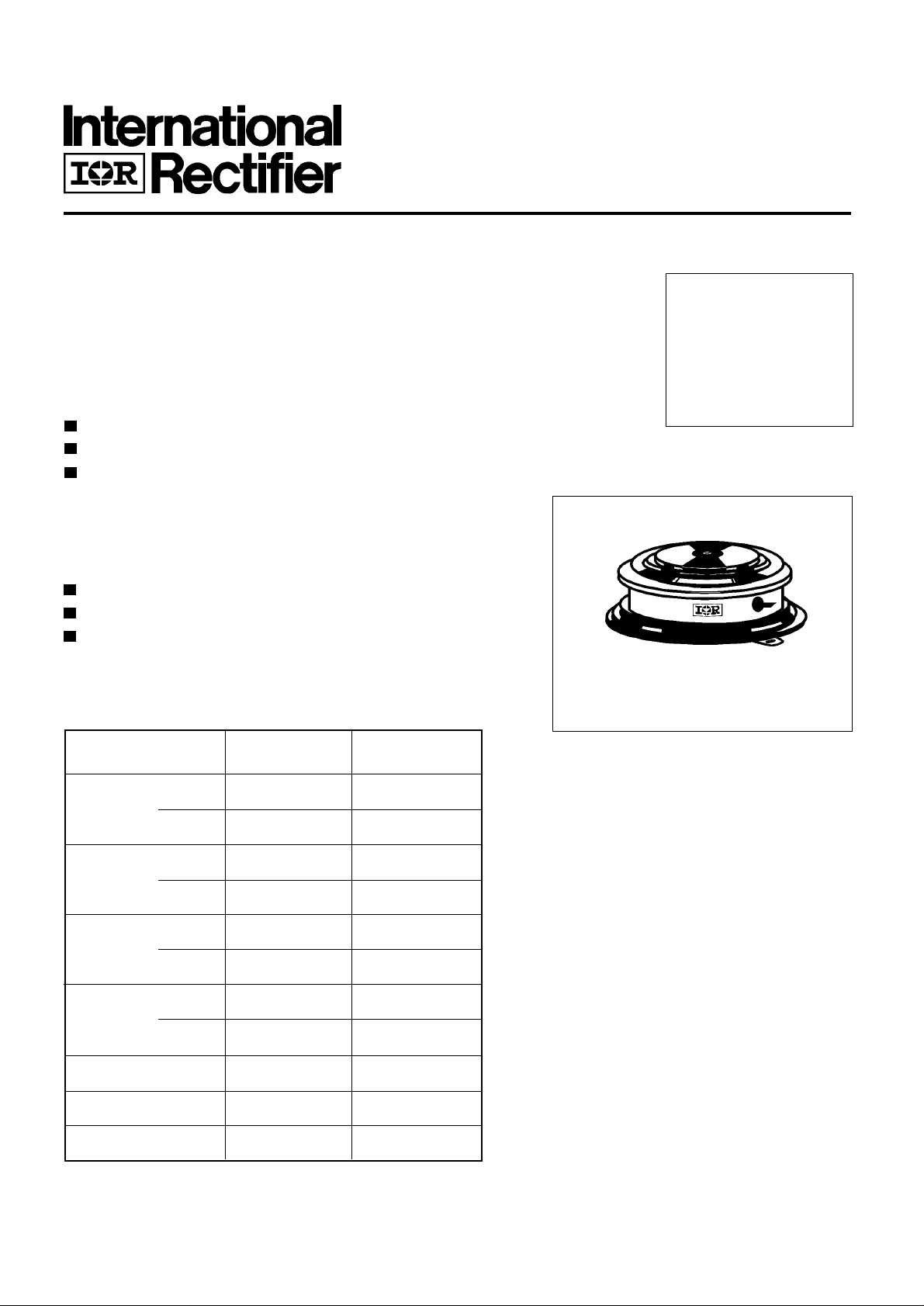
ST230C..C SERIES
PHASE CONTROL THYRISTORS Hockey Puk V ersion
410A
Features
Center amplifying gate
Metal case with ceramic insulator
International standard case TO-200AB (A-PUK)
Typical Applications
DC motor controls
Controlled DC power supplies
AC controllers
Major Ratings and Characteristics
Parameters ST230C..C Units
I
T(AV)
I
T(RMS)
I
TSM
@ T
hs
@ T
hs
@ 50Hz 5700 A
@ 60Hz 5970 A
410 A
55 °C
780 A
25 °C
case style TO-200AB (A-PUK)
I2t@
V
DRM/VRRM
t
q
T
J
50Hz 163 KA2s
@ 60Hz 149 KA2s
typical 100 µs
400 to 1600 V
- 40 to 125 °C
ST230C..C Series
Next Data SheetIndex
Previous Datasheet
To Order
ELECTRICAL SPECIFICATIONS
Voltage Ratings
Voltage V
DRM/VRRM
Type number Code peak and off-state voltage repetitive peak voltage @ T
, max. repetitive V
, maximum non- I
RSM
DRM/IRRM
J
VVmA
04 400 500
08 800 900
ST230C..C 12 1200 1300 30
14 1400 1500
16 1600 1700
On-state Conduction
Parameter ST230C..C Units Conditions
I
T(AV)
I
T(RMS)
I
TSM
2
t Maximum I2t for fusing 163 t = 10ms No voltage Initial TJ = TJ max.
I
2
I
V
V
Max. average on-state current 410 (165) A 180° conduction, half sine wave
@ Heatsink temperature 55 (85) °C double side (single side) cooled
Max. RMS on-state current 780 DC @ 25°C heatsink temperature double side cooled
Max. peak, one-cycle 5700 t = 10ms No voltage
non-repetitive surge current 5970 A t = 8.3ms reapplied
4800 t = 10ms 100% V
RRM
5000 t = 8.3ms reapplied Sinusoidal half wave,
148 t = 8.3ms reapplied
KA2s
115 t = 10ms 100% V
RRM
105 t = 8.3ms reapplied
√t Maximum I2√t for fusing 1630 KA2√s t = 0.1 to 10ms, no voltage reapplied
Low level value of threshold
T(TO)
1
voltage
0.92 (16.7% x π x I
< I < π x I
T(AV)
), TJ = TJ max.
T(AV)
V
High level value of threshold
T(TO)
2
voltage
0.98 (I > π x I
),TJ = TJ max.
T(AV)
max.
= TJ max
r
Low level value of on-state
t1
slope resistance
r
High level value of on-state
t2
slope resistance
V
I
H
I
L
Max. on-state voltage 1.69 V Ipk= 880A, TJ = TJ max, tp = 10ms sine pulse
TM
Maximum holding current 600
Max. (typical) latching current 1000 (300)
Switching
Parameter ST230C..C Units Conditions
di/dt Max. non-repetitive rate of rise Gate drive 20V, 20Ω, tr ≤ 1µs
of turned-on current T
t
d
Typical delay time 1.0
t
q
Typical turn-off time 100
0.88 (16.7% x π x I
mΩ
0.81 (I > π x I
T(AV)
mA TJ = 2 5 ° C , anode supply 12V resistive load
1000 A/µs
= TJ max, anode voltage ≤ 80% V
J
Gate current 1A, d ig/dt = 1A/µs
= 0.67% V
V
µs
d
I
= 300A, TJ = TJ max, di/dt = 20A/µs, VR = 50V
TM
= 20V/µs, Gate 0V 100Ω, tp = 500µs
dv/dt
< I < π x I
T(AV)
),TJ = TJ max.
= 25°C
DRM, TJ
), TJ = TJ max.
T(AV)
DRM
Blocking
To Order
Next Data SheetIndex
Previous Datasheet
ST230C..C Series
Parameter ST230C..C Units Conditions
dv/dt Maximum critical rate of rise of
I
DRM
I
RRM
Max. peak reverse and off-state
leakage current
Triggering
Parameter ST230C..C Units Conditions
P
P
I
+V
-V
I
V
I
V
Maximum peak gate power 10.0 TJ = TJ max, tp ≤ 5ms
GM
Maximum average gate power 2.0 TJ = TJ max, f = 50Hz, d% = 50
G(AV)
Max. peak positive gate current 3.0 A TJ = TJ max, tp ≤ 5ms
GM
Maximum peak positive
GM
gate voltage
Maximum peak negative
GM
gate voltage
DC gate current required
GT
to trigger
DC gate voltage required
GT
to trigger
DC gate current not to trigger 10 mA
GD
DC gate voltage not to trigger 0.25 V
GD
500 V/µ sTJ = TJ max. linear to 80% rated V
off-state voltage
30 mA TJ = TJ max, rated V
W
20
VT
= TJ max, tp ≤ 5ms
J
5.0
TYP. MAX.
180 -
90 150
40 -
2.9 -
1.8 3.0
1.2 -
mA T
VTJ = 25°C
= - 40°C
T
J
= 25°C
J
TJ = 125°C
TJ = - 40°C
= 125°C
T
J
Max. required gate trigger/ current/ voltage are the lowest value
which will trigger all units 12V
anode-to-cathode applied
Max. gate current/voltage not to
T
= TJ max
J
trigger is the max. value which
will not trigger any unit with rated
V
DRM
DRM
DRM/VRRM
applied
anode-to-cathode applied
Thermal and Mechanical Specification
Parameter ST230C..C Units Conditions
Max. operating temperature range -40 to 125
T
J
Max. storage temperature range -40 to 150
T
stg
R
Max. thermal resistance, 0.17 D C operation single side cooled
thJ-hs
junction to heatsink 0.08 DC operation double side cooled
Max. thermal resistance, 0.033 DC operation single side cooled
R
thC-hs
case to heatsink 0.017 DC operation double side cooled
F Mounting force, ± 10% 4900 N
wt Approximate weight 50 g
Case style TO - 200AB (A-PUK) See Outline Table
°C
K/W
K/W
(500) (Kg)
 Loading...