


IRFPS3810
PD - 93912A
IRFPS3810
HEXFET® Power MOSFET
l Advanced Process Technology
l Ultra Low On-Resistance
l Dynamic dv/dt Rating
l 175°C Operating Temperature
l Fast Switching
l Fully Avalanche Rated
Description
G
D
V
= 100V
DSS
R
S
= 0.009Ω
DS(on)
= 170A
I
D
The HEXFET® Power MOSFETs from International
Rectifier utilize advanced processing techniques to
achieve extremely low on-resistance per silicon area.
This benefit, combined with the fast switching speed
and ruggedized device design that HEXFET power
MOSFETs are well known for, provides the designer
with an extremely efficient and reliable device for use in
a wide variety of applications.
Super-247™
Absolute Maximum Ratings
Parameter Max. Units
ID @ TC = 25°C Continuous Drain Current, VGS @ 10V 170
ID @ TC = 100°C Continuous Drain Current, VGS @ 10V 120 A
I
DM
PD @TC = 25°C Power Dissipation 580 W
V
GS
E
AS
I
AR
E
AR
dv/dt Peak Diode Recovery dv/dt 2.3 V/ns
T
J
T
STG
Pulsed Drain Current 670
Linear Derating Factor 3.8 W/°C
Gate-to-Source Voltage ± 30 V
Single Pulse Avalanche Energy 1350 mJ
Avalanche Current 100 A
Repetitive Avalanche Energy 58 mJ
Operating Junction and -55 to + 175
Storage Temperature Range
Soldering Temperature, for 10 seconds 300 (1.6mm from case )
°C
Thermal Resistance
Parameter Typ. Max. Units
R
θJC
R
θCS
R
θJA
Junction-to-Case ––– 0.26
Case-to-Sink, Flat, Greased Surface 0.24 ––– °C/W
Junction-to-Ambient ––– 40
www.irf.com 1
1/21/02
IRFPS3810
APPROVED
Electrical Characteristics @ TJ = 25°C (unless otherwise specified)
Parameter Min. Typ. Max. Units Conditions
V
(BR)DSS
∆V
(BR)DSS
R
DS(on)
V
GS(th)
g
fs
I
DSS
I
GSS
Q
g
Q
gs
Q
gd
t
d(on)
t
r
t
d(off)
t
f
L
D
L
S
C
iss
C
oss
C
rss
C
oss
C
oss
C
eff. Effective Output Capacitance ––– 2210 ––– VGS = 0V, VDS = 0V to 80V
oss
Drain-to-Source Breakdown Voltage 100 ––– ––– VVGS = 0V, ID = 250µA
/∆T
Breakdown Voltage Temp. Coefficient ––– 0.11 ––– V/°C Reference to 25°C, ID = 1mA
J
Static Drain-to-Source On-Resistance ––– ––– 0.009 Ω VGS = 10V, ID = 100A
Gate Threshold Voltage 3.0 ––– 5.0 V VDS = 10V, ID = 250µA
Forward Transconductance 52 ––– ––– SVDS = 50V, ID = 100A
Drain-to-Source Leakage Current
––– ––– 25
––– ––– 250 VDS = 80V, VGS = 0V, TJ = 150°C
Gate-to-Source Forward Leakage ––– ––– 100 V
Gate-to-Source Reverse Leakage ––– ––– -100
VDS = 100V, VGS = 0V
µA
= 30V
GS
nA
VGS = -30V
Total Gate Charge ––– 260 390 ID = 100A
Gate-to-Source Charge ––– 49 74 nC VDS = 80V
Gate-to-Drain ("Miller") Charge ––– 160 250 VGS = 10V
Turn-On Delay Time ––– 24 ––– VDD = 50V
Rise Time ––– 270 ––– ID = 100A
Turn-Off Delay Time ––– 45 ––– RG = 1.03Ω
ns
Fall Time ––– 140 ––– VGS = 10V
Internal Drain Inductance
Internal Source Inductance ––– –––
––– –––
5.0
13
Between lead,
6mm (0.25in.)
nH
from package
and center of die contact
Input Capacitance ––– 6790 ––– VGS = 0V
Output Capacitance ––– 2470 ––– pF VDS = 25V
Reverse Transfer Capacitance ––– 990 ––– ƒ = 1.0MHz, See Fig. 5
Output Capacitance ––– 10740 ––– VGS = 0V, VDS = 1.0V, ƒ = 1.0MHz
Output Capacitance ––– 1180 ––– VGS = 0V, VDS = 80V, ƒ = 1.0MHz
D
G
S
Source-Drain Ratings and Characteristics
Parameter Min. Typ. Max. Units Conditions
I
S
I
SM
V
SD
t
rr
Q
rr
t
on
Continuous Source Current MOSFET symbol
(Body Diode)
Pulsed Source Current integral reverse
(Body Diode)
––– –––
––– –––
170
670
showing the
A
p-n junction diode.
G
Diode Forward Voltage ––– ––– 1.3 V TJ = 25°C, IS = 100A, VGS = 0V
Reverse Recovery Time ––– 220 330 ns TJ = 25°C, IF = 100A
Reverse RecoveryCharge ––– 1640 2460 nC di/dt = 100A/µs
Forward Turn-On Time Intrinsic turn-on time is negligible (turn-on is dominated by LS+LD)
Notes:
Repetitive rating; pulse width limited by
max. junction temperature. (See fig. 11)
Starting T
RG = 25Ω, I
I
SD
= 25°C, L = 0.27mH
J
= 100A. (See Figure 12)
AS
≤ 100A, di/dt ≤ 350A/µs, V
DD
≤ V
(BR)DSS
Pulse width ≤ 400µs; duty cycle ≤ 2%.
C
eff. is a fixed capacitance that gives the same charging time
oss
as C
Calculated continuous current based on maximum allowable
,
junction temperature. Package limitation current is 105A.
oss
while V
is rising from 0 to 80% V
DS
DSS
TJ ≤ 175°C
2 www.irf.com
D
S
APPROVED
IRFPS3810
1000
100
10
1
TOP
BOTTOM
VGS
15V
12V
10V
8.0V
7.0V
6.0V
5.5V
5.0V
5.0V
0.1
D
I , Drain-to-Source Current (A)
50µs PULSE WIDTH
°
T = 25 C
0.01
0.1 1 10 100
V , Drain-to-Sou rce Voltage (V)
DS
1000
J
1000
100
10
D
I , Drain-to-Source Current (A)
1
0.1 1 10 100
VGS
TOP
15V
12V
10V
8.0V
7.0V
6.0V
5.5V
BOTTOM
5.0V
5.0V
50µs PULSE WIDTH
T = 175 C
J
V , Drain-to-Source Voltage (V)
DS
°
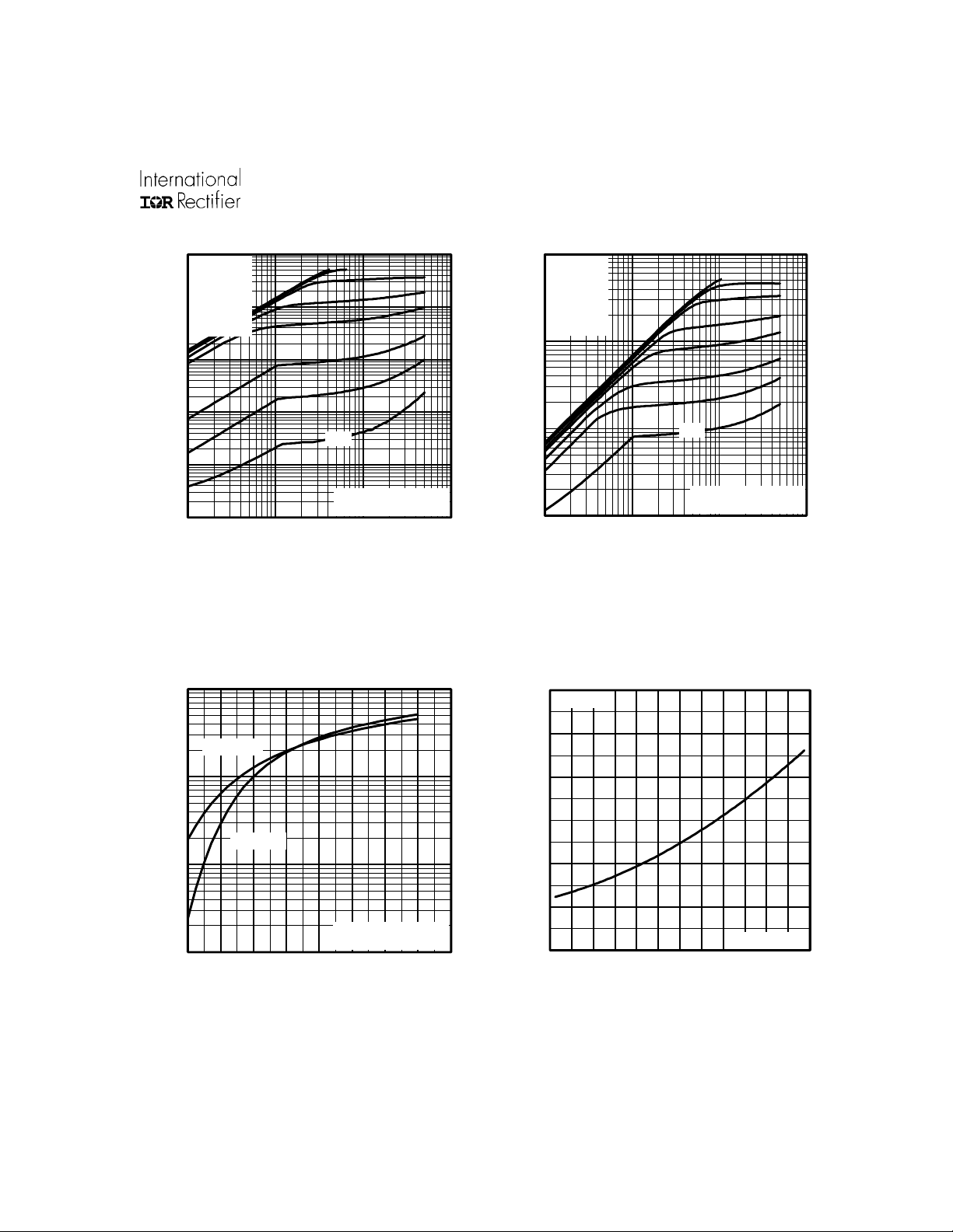
Fig 2. Typical Output CharacteristicsFig 1. Typical Output Characteristics
3.0
I =
D
170A
°
T = 175 C
J
100
°
T = 25 C
J
10
D
I , Drain-to-Source Current (A)
V = 50V
DS
1
5 6 7 8 9 10 11 12 13
V , Gate-to-Source Voltage (V)
GS
50µs PULSE WIDTH
Fig 3. Typical Transfer Characteristics
2.5
2.0
1.5
(Normalized)
1.0
0.5
DS(on)
R , Drain-to-Source On Resistance
0.0
-60 -40 -20 0 20 40 60 80 100 120 140 160 180
T , Junction Temperature ( C)
J
Fig 4. Normalized On-Resistance
V =
GS
°
10V
Vs. Temperature
www.irf.com 3
 Loading...