


IR2113-2
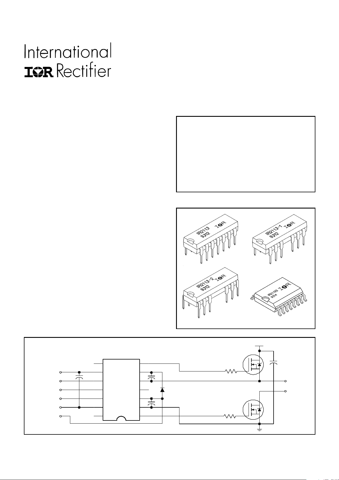
Typical Connection
Features
n Floating channel designed for bootstrap operation
Fully operational to +600V
Tolerant to negative transient voltage
dV/dt immune
n Gate drive supply range from 10 to 20V
n Undervoltage lockout for both channels
n Separate logic supply range from 5 to 20V
Logic and power ground ±5V offset
n CMOS Schmitt-triggered inputs with pull-down
n Cycle by cycle edge-triggered shutdown logic
n Matched propagation delay for both channels
n Outputs in phase with inputs
Description
The IR2113 is a high voltage, high speed power
MOSFET and IGBT driver with independent high and
low side referenced output channels. Proprietary
HVIC and latch immune CMOS technologies enable
ruggedized monolithic construction. Logic inputs are
compatible with standard CMOS or LSTTL outputs.
The output drivers feature a high pulse current b uff er
stage designed for minimum driver cross-conduc-
tion. Propagation delays are matched to simplify
use in high frequency applications. The floating
channel can be used to drive an N-channel power
MOSFET or IGBT in the high side configuration
which operates up to 600 volts.
Packages
Data Sheet No. PD-6.030C
IR2113
HIGH AND LOW SIDE DRIVER
Product Summary
V
OFFSET
600V max.
I
O
+/- 2A / 2A
V
OUT
10 - 20V
t
on/off
(typ.) 120 & 94 ns
Delay Matching 10 ns
HIN
up to 600V
TO
LOAD
V
DD
V
B
V
S
HO
LO
COM
HIN
LIN
V
SS
SD
V
CC
LIN
V
DD
SD
V
SS
V
CC
CONTROL INTEGRATED CIRCUIT DESIGNERS MANUAL B-61
IR2113
B-62 CONTROL INTEGRATED CIRCUIT DESIGNERS MANUAL
Parameter Value
Symbol Definition Min. Max. Units
V
B
High Side Floating Supply Voltage -0.3 625
V
S
High Side Floating Supply Offset Voltage V
B
- 25 V
B
+ 0.3
V
HO
High Side Floating Output Voltage V
S
- 0.3 V
B
+ 0.3
V
CC
Low Side Fixed Supply Voltage -0.3 25
V
LO
Low Side Output Voltage -0.3 V
CC
+ 0.3
V
DD
Logic Supply Voltage -0.3 V
SS
+ 25
V
SS
Logic Supply Offset Voltage V
CC
- 25 V
CC
+ 0.3
V
IN
Logic Input Voltage (HIN, LIN & SD) V
SS
- 0.3 V
DD
+ 0.3
dV
s
/dt Allowable Offset Supply Voltage Transient (Figure 2) — 50 V/ns
P
D
Package Power Dissipation @ T
A
≤ +25°C (14 Lead DIP) — 1.6
(14 Lead DIP w/o Lead 4) — 1.5
(16 Lead DIP w/o Leads 5 & 6) — 1.6
(16 Lead SOIC) — 1.25
R
θJA
Thermal Resistance, Junction to Ambient (14 Lead DIP) — 75
(14 Lead DIP w/o Lead 4) — 85
(16 Lead DIP w/o Leads 5 & 6) — 75
(16 Lead SOIC) — 100
T
J
Junction Temperature — 1 50
T
S
Storage Temperature -55 15 0 °C
T
L
Lead Temperature (Soldering, 10 seconds) — 30 0
Parameter Value
Symbol Definition Min. Max. Units
V
B
High Side Floating Supply Absolute Voltage V
S
+ 10 V
S
+ 20
V
S
High Side Floating Supply Offset Voltage Note 1 600
V
HO
High Side Floating Output Voltage V
S
V
B
V
CC
Low Side Fixed Supply Voltage 10 20
V
LO
Low Side Output Voltage 0 V
CC
V
DD
Logic Supply Voltage V
SS
+ 5 V
SS
+ 20
V
SS
Logic Supply Offset Voltage -5 5
V
IN
Logic Input Voltage (HIN, LIN & SD) V
SS
V
DD
T
A
Ambient Temperature -40 12 5 °C
Absolute Maximum Ratings
Absolute Maximum Ratings indicate sustained limits beyond which damage to the device may occur. All voltage param-
eters are absolute voltages referenced to COM. The Thermal Resistance and Power Dissipation ratings are measured
under board mounted and still air conditions. Additional information is shown in Figures 28 through 35.
Recommended Operating Conditions
The Input/Output logic timing diagram is shown in Figure 1. F or proper operation the de vice should be used within the
recommended conditions. The V
S
and V
SS
offset ratings are tested with all supplies biased at 15V differential.
Typical ratings at other bias conditions are shown in Figures 36 and 37.
Note 1: Logic operational for V
S
of -5 to +600V. Logic state held for V
S
of -5V to -V
BS
.
°C/W
W
V
V
IR2113
CONTROL INTEGRATED CIRCUIT DESIGNERS MANUAL B-63
Parameter Value
Symbol Definition Figure Min. Typ. Max. Units Test Conditions
t
on
Turn-On Propagation Delay 7 — 120 150 V
S
= 0V
t
off
Turn-Off Propagation Delay 8 — 94 125 V
S
= 600V
t
sd
Shutdown Propagation Delay 9 — 110 140 V
S
= 600V
t
r
Turn-On Rise Time 10 — 25 35
t
f
Turn-Off Fall Time 11 — 17 25
MT Delay Matching, HS & LS Turn-On/Off — — — 10 Figure 5
Parameter Value
Symbol Definition Figure Min. Typ. Max. Units Test Conditions
V
IH
Logic “1” Input Voltage 12 9.5 — —
V
IL
Logic “0” Input Voltage 13 — — 6.0
V
OH
High Level Output V oltage, V
BIAS
- V
O
14 — — 1.2 I
O
= 0A
V
OL
Low Level Output V oltage, V
O
15 — — 0.1 I
O
= 0A
I
LK
Offset Supply Leakage Current 16 — — 50 V
B
= V
S
= 600V
I
QBS
Quiescent V
BS
Supply Current 17 — 125 230 V
IN
= 0V or V
DD
I
QCC
Quiescent V
CC
Supply Current 18 — 180 340 V
IN
= 0V or V
DD
I
QDD
Quiescent V
DD
Supply Current 19 — 15 30 V
IN
= 0V or V
DD
I
IN+
Logic “1” Input Bias Current 20 — 2 0 40 V
IN
= V
DD
I
IN-
Logic “0” Input Bias Current 21 — — 1.0 V
IN
= 0V
V
BSUV+
V
BS
Supply Undervoltage Positive Going 2 2 7.5 8.6 9.7
Threshold
V
BSUV-
V
BS
Supply Undervoltage Negative Going 23 7.0 8.2 9.4
Threshold
V
CCUV+
V
CC
Supply Undervoltage Positive Going 24 7.4 8.5 9.6
Threshold
V
CCUV-
V
CC
Supply Undervoltage Negative Going 25 7.0 8.2 9.4
Threshold
I
O+
Output High Short Circuit Pulsed Current 26 2.0 2.5 — V
O
= 0V, V
IN
= V
DD
PW ≤ 10 µs
I
O-
Output Low Short Circuit Pulsed Current 27 2.0 2.5 — V
O
= 15V, V
IN
= 0V
PW ≤ 10 µ s
ns
Dynamic Electrical Characteristics
V
BIAS
(V
CC
, V
BS
, V
DD
) = 15V, C
L
= 1000 pF, T
A
= 25°C and V
SS
= COM unless otherwise specified. The dynamic
electrical character istics are measured using the test circuit shown in Figure 3.
Static Electrical Characteristics
V
BIAS
(V
CC
, V
BS
, V
DD
) = 15V, T
A
= 25°C and V
SS
= COM unless otherwise specified. The V
IN
, V
TH
and I
IN
parameters
are referenced to V
SS
and are applicable to all three logic input leads: HIN, LIN and SD. The V
O
and I
O
parameters are
referenced to COM and are applicable to the respective output leads: HO or LO.
µA
V
A
V
IR2113
B-64 CONTROL INTEGRATED CIRCUIT DESIGNERS MANUAL
Lead
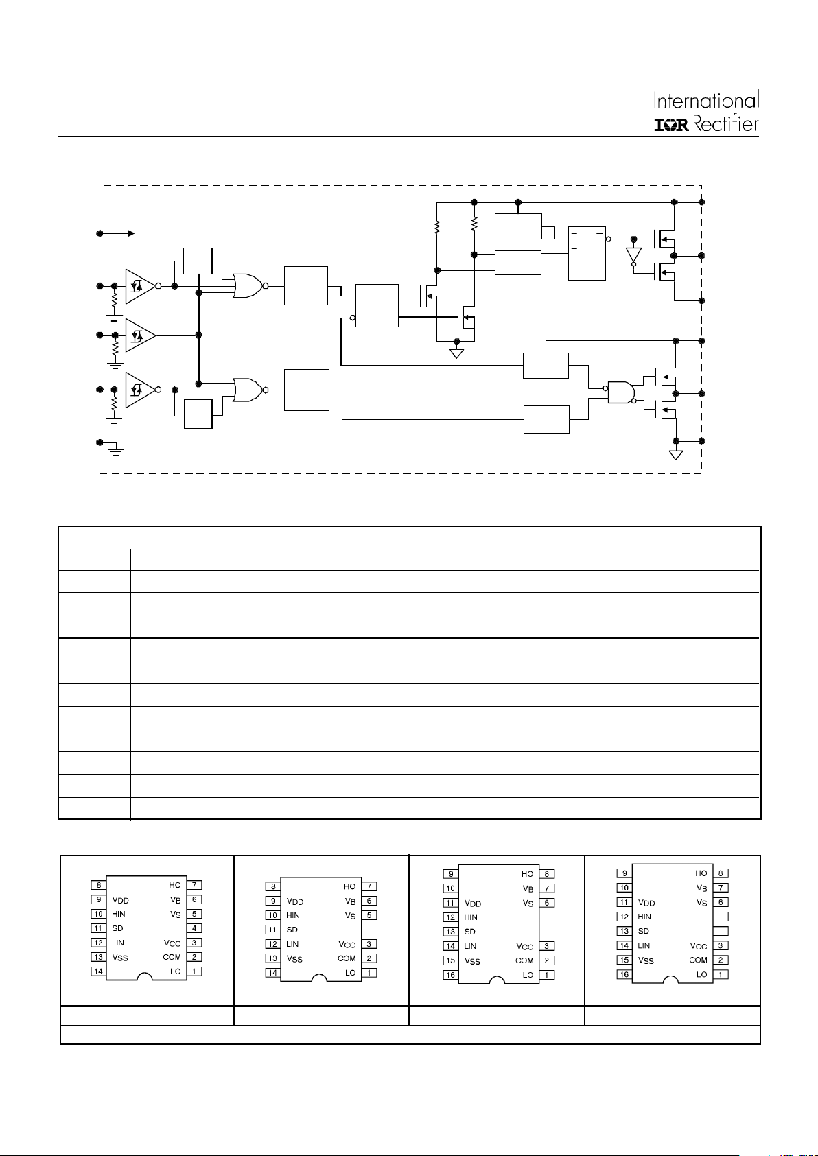
Symbol Description
V
DD
Logic supply
HIN Logic input for high side gate driver output (HO), in phase
SD Logic input for shutdown
LIN Logic input for low side gate driver output (LO), in phase
V
SS
Logic ground
V
B
High side floating supply
HO High side gate drive output
V
S
High side floating supply return
V
CC
Low side supply
LO Low side gate drive output
COM Low side return
Functional Block Diagram
Lead Definitions
Lead Assignments
14 Lead DIP 14 Lead DIP w/o Lead 4 16 Lead DIP w/o Leads 4 & 5 16 Lead SOIC (Wide Body)
IR2113 IR2113-1 IR2113-2 IR2113S
P art Number
V
B
SD
LIN
V
DD
PULSE
GEN
R
S
Q
V
SS
UV
DETECT
DELAY
HV
LEVEL
SHIFT
V
CC
PULSE
FILTER
UV
DETECT
V
DD
/V
CC
LEVEL
SHIFT
V
DD
/V
CC
LEVEL
SHIFT
LO
V
S
COM
R
S
Q
R
S
RQ
HIN
HO
IR2113
CONTROL INTEGRATED CIRCUIT DESIGNERS MANUAL B-65
Thickness of Gate Oxide 800Å
Connections Material P oly Silicon
First Width 4 µm
La yer Spacing 6 µm
Thickness 5000Å
Material Al - Si (Si: 1.0% ±0.1%)
Second Width 6 µm
La yer Spacing 9 µm
Thickness 20,000Å
Contact Hole Dimension 8 µm X 8 µm
Insulation Layer Material PSG (SiO
2
)
Thickness 1.5 µm
P assivation Material PSG (SiO
2
)
Thickness 1.5 µm
Method of Saw Full Cut
Method of Die Bond Ablebond 84 - 1
Wire Bond Method Thermo Sonic
Material Au (1.0 mil / 1.3 mil)
Leadframe Material Cu
Die Area Ag
Lead Plating Pb : Sn (37 : 63)
P ackage Types 14 & 16 Lead PDIP / 16 Lead SOIC
Materials EME6300 / MP150 / MP190
Remarks:
Device Information
Process & Design Rule HVDCMOS 4.0 µ m
Transistor Count 220
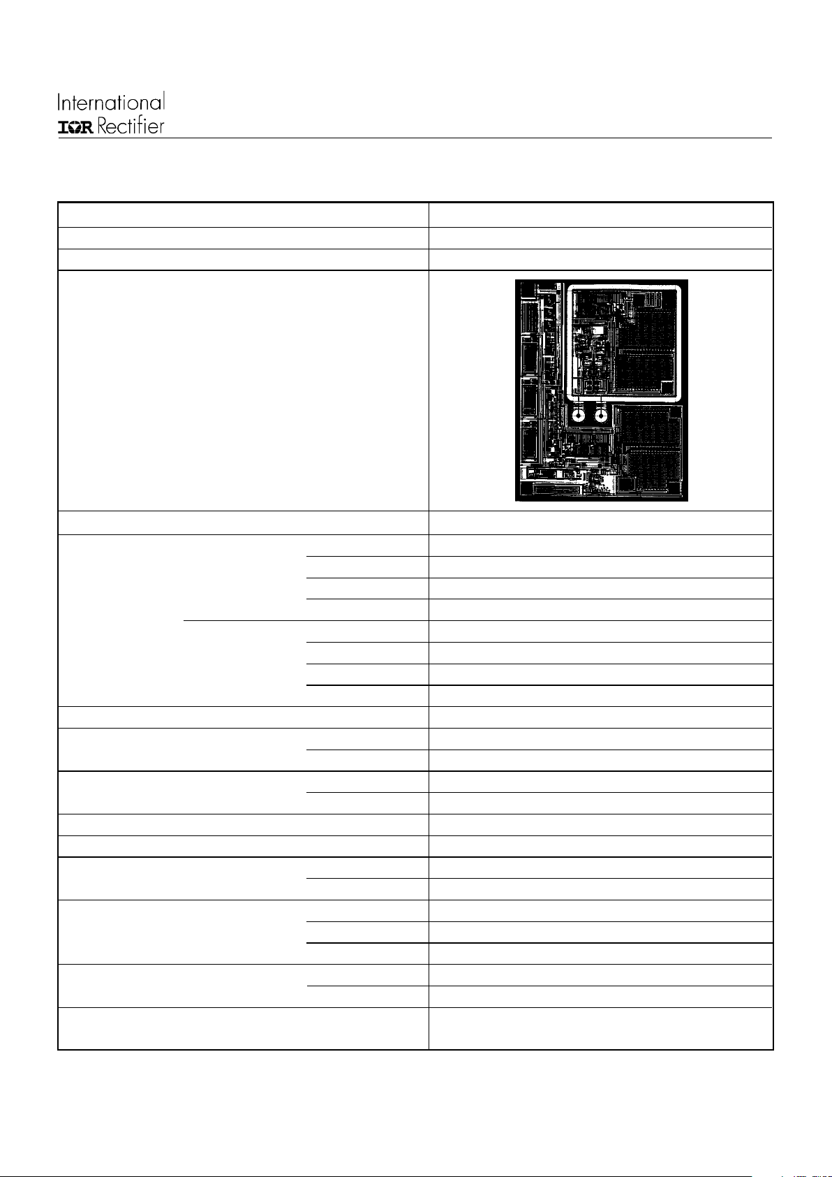
Die Siz e 98 X 126 X 26 (mil)
Die Outline
 Loading...