


International Rectifier IRU1207-33CS, IRU1207-25CS, IRU1207-18CS, IRU1206-33CY, IRU1206-33CD Datasheet
...
|
Data Sheet No. PD94134 |
|
IRU1206 / IRU1207 / IRU1208 / IRU1209 |
|
|
|
|
|
1A VERY LOW DROPOUT POSITIVE |
|
FIXED AND ADJUSTABLE REGULATORS |
FEATURES |
DESCRIPTION |
Low Dropout Voltage (500mV at 1A) 1% Voltage Reference Accuracy Low Ground Current
1µA Maximum Quiescent Current in Shutdown (IRU1207, IRU1208)
Fast Transient Response
Current Limit and Thermal Shutdown
Error Flag Signal for Output out of Regulation (IRU1207, IRU1208)
APPLICATIONS
2.5V Supply from 3.3V Input for the new generation of Logic ICs
Computer Mother Board, Add-On Cards
High Efficiency Post Regulator in Switch Mode Power Supply (SMPS)
The IRU1206 family of devices are ultra low dropout 1A regulators using PNP transistor as the pass element. These products are ideal when a single input supply is only available and the dropout voltage is less than 1V, exceeding the minimum dropout characteristics of NPN/ PNP hybrid regulators. One common application of these regulators is where input is 3.3V and a 2.5V output is needed.
Besides the low dropout of less than 0.5V, other features of the family of the parts are: micro-power shutdown capability and output UVLO detection where Flag pin is switched low when output is below 5% of its nominal point.
TYPICAL APPLICATION
Vout 3
IRU1206-
XX Gnd 2 
Vin 1
Vin
C1
Vout
C2
1206app2-1.0
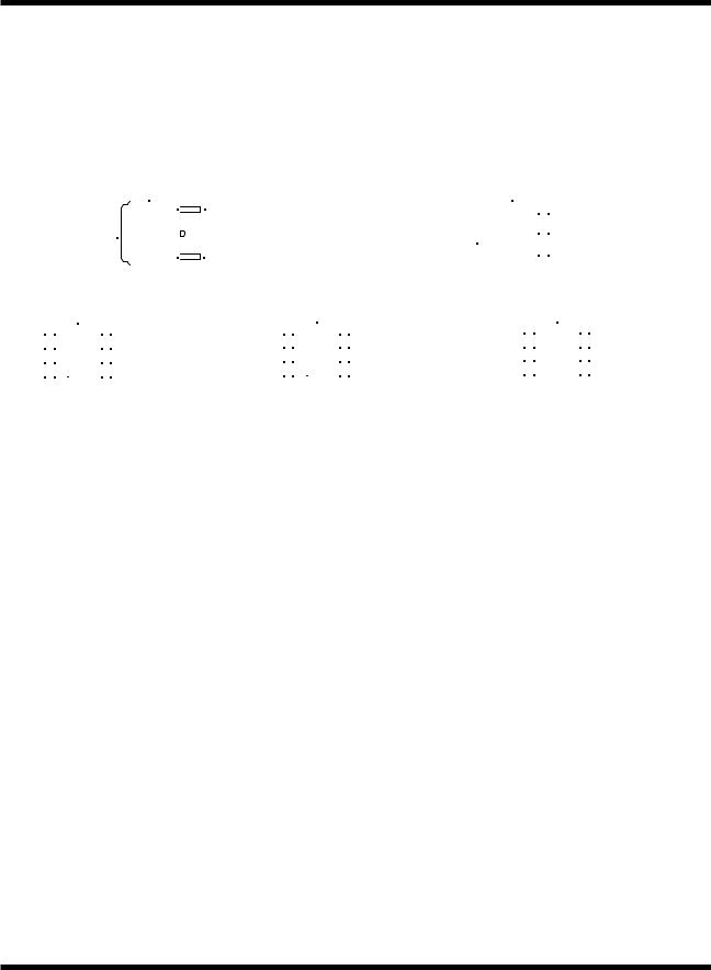
Figure 1 - Typical application of the 1206-XX in a 3-Pin SOT-223 package.
PACKAGE ORDER INFORMATION
TJ (°C) |
2-PIN TO-252 |
3-PIN |
8-PIN PLASTIC |
VOLTAGE |
PIN FUNCTIONS |
|
(D-PAK) |
SOT-223 (Y) |
SOIC POWER (S) |
|
|
0 To 125 |
IRU1206-18CD |
IRU1206-18CY |
NA |
1.8V |
VIN, VOUT, Gnd |
0 To 125 |
IRU1206-25CD |
IRU1206-25CY |
NA |
2.5V |
VIN, VOUT, Gnd |
0 To 125 |
IRU1206-33CD |
IRU1206-33CY |
NA |
3.3V |
VIN, VOUT, Gnd |
0 To 125 |
NA |
NA |
IRU1207-18CS |
1.8V |
VIN, VOUT, Gnd, Enable, Flag |
0 To 125 |
NA |
NA |
IRU1207-25CS |
2.5V |
VIN, VOUT, Gnd, Enable, Flag |
0 To 125 |
NA |
NA |
IRU1207-33CS |
3.3V |
VIN, VOUT, Gnd, Enable, Flag |
0 To 125 |
NA |
NA |
IRU1208CS |
Adj |
VIN, VOUT, Gnd, Flag, Adj |
0 To 125 |
NA |
NA |
IRU1209CS |
Adj |
VIN, VOUT, Gnd, Enable, Adj |
|
|
|
|
|
|
|
|
|
|
|
|
Rev. 1.8 |
1 |
09/07/01 |
IRU1206 / IRU1207 / IRU1208 / IRU1209
ABSOLUTE MAXIMUM RATINGS
Input Voltage (VIN) .................................................... |
12V |
Enable Input Voltage ................................................ |
12V |
Storage Temperature Range ...................................... |
-65°C To 150°C |
Operating Junction Temperature Range ..................... |
0°C To 135°C |
|
|
|
|
PACKAGE INFORMATION
|
|
|
3-PIN PLASTIC TO-252 (D-Pak) |
|
|
|
|
|
|
|
3-PIN PLASTIC SOT-223 (Y) |
||||||||||||||||
|
|
|
|
|
IRU1206 |
|
|
|
|
|
|
|
|
|
|
|
IRU1206 |
|
|
|
|
||||||
|
|
|
|
|
|
FRONT VIEW |
|
|
|
|
|
|
|
|
|
|
|
|
TOP VIEW |
|
|
|
|
||||
|
|
|
|
|
|
3 |
|
Vout |
|
|
|
|
|
|
|
|
|
|
|
|
|
|
Vout |
|
|||
|
|
|
|
|
|
|
|
|
|
|
|
|
|
|
|
|
|
|
3 |
|
|||||||
|
|
|
|
Tab is |
|
|
|
θ JA=70° C/W for |
|
|
|
|
Tab is |
|
|
|
|
|
Gnd |
θ JA=90° C/W for |
|||||||
|
|
|
|
Gnd |
|
|
|
|
|
|
|
Gnd |
|
|
|
2 |
|||||||||||
|
|
|
|
|
|
|
|
|
|
|
|
|
|
||||||||||||||
|
|
|
|
|
|
|
|
|
0.5" Sq pad |
|
|
|
|
|
|
|
|
|
|
|
Vin |
0.4" Sq pad |
|||||
|
|
|
|
|
|
1 |
|
Vin |
|
|
|
|
|
|
|
|
|
1 |
|||||||||
|
|
|
|
|
|
|
|
|
|
|
|
|
|
|
|
|
|
|
|
|
|
|
|
|
|
|
|
|
|
|
|
|
|
|
|
|
8-PIN PLASTIC POWER SOIC (S) |
|
|
|
|
|
|
|
|
|
|||||||||
|
IRU1207 |
|
|
|
|
IRU1208 |
|
|
|
|
|
|
IRU1209 |
|
|||||||||||||
|
|
TOP VIEW |
|
|
|
|
|
|
TOP VIEW |
|
|
|
|
|
|
|
|
|
|
TOP VIEW |
|
|
|||||
Enable |
|
|
|
|
Gnd |
|
|
|
Flag |
|
|
|
|
|
Gnd |
|
|
|
Enable |
|
|
|
|
|
|
Gnd |
|
1 |
|
|
8 |
|
|
|
1 |
|
|
8 |
|
|
|
1 |
|
|
8 |
|
|||||||||
Vin |
|
|
|
|
Gnd |
|
|
|
Vin |
|
|
|
|
|
Gnd |
|
|
|
Vin |
|
|
|
|
|
|
Gnd |
|
2 |
|
|
7 |
|
|
|
2 |
|
|
7 |
|
|
|
2 |
|
|
7 |
|
|||||||||
Vout |
|
|
|
|
Gnd |
θ JA=55° C/W |
Vout |
|
|
|
|
|
Gnd |
θ JA=55° C/W |
|
|
Vout |
|
|
|
|
|
|
Gnd θ JA=55° C/W |
|||
3 |
|
|
6 |
3 |
|
|
6 |
|
3 |
|
|
6 |
|
||||||||||||||
Flag |
|
|
|
|
Gnd |
for 1" Sq pad |
Adj |
|
|
|
|
|
Gnd |
for 1" Sq pad |
|
|
Adj |
|
|
|
|
|
|
Gnd for 1" Sq pad |
|||
4 |
|
|
5 |
4 |
|
|
5 |
|
4 |
|
|
5 |
|
||||||||||||||
|
|
|
|
|
|
|
|
|
|
|
|||||||||||||||||
|
|
|
|
|
|
|
|
|
|
|
|
|
|
|
|
|
|
|
|
|
|
|
|
|
|
|
|
|
|
|
|
|
|
|
|
|
|
|
|
|
|
|
|
|
|
|
|
|
|
|
|
|
|
|
|
|
|
|
|
|
|
|
|
|
|
|
|
|
|
|
|
|
|
|
|
|
|
|
|
|
|
|
|
ELECTRICAL SPECIFICATIONS
Unless otherwise specified, these specifications apply over CIN=COUT=10µF, VIN=Vo+1V, VOUT=VFB (For adjustable version only), and TA=25°C. Typical values refer to TA=25°C. Low duty cycle pulse testing is used which keeps junction and case temperatures equal to the ambient temperature.
PARAMETER |
SYM |
TEST CONDITION |
MIN |
TYP |
MAX |
UNITS |
Initial Voltage Accuracy |
Vo |
Io=10mA, TA=25"C |
-1 |
|
1 |
% |
See Table 1 for nominal values |
|
(Note 4) |
-1.3 |
|
1.3 |
|
Line Regulation |
∆VI |
Vo + 1V<VIN<12 |
|
0.5 |
1 |
% |
Load Regulation (Note 1) |
∆VL |
10mA<Io<1A |
|
0.5 |
0.7 |
% |
|
|
1mA<Io<150mA |
|
|
0.5 |
% |
Output Voltage Temp Coef. |
∆VO(T) |
|
|
20 |
100 |
ppm/"C |
Dropout Voltage (Note 2) |
∆VI(O) |
Io=100mA (Note 4) |
|
100 |
200 |
mV |
|
|
Io=500mA (Note 4) |
|
300 |
400 |
|
|
|
Io=1000mA (Note 4) |
|
500 |
650 |
|
Ground Current (Note 3) |
IQ |
VIN=Vo + 1 for all conditions: |
|
|
|
|
|
|
Io=100mA (Note 4) |
|
|
3 |
mA |
|
|
Io=500mA (Note 4) |
|
|
15 |
|
|
|
Io=1000mA (Note 4) |
|
|
50 |
|
Current Limit |
ICL |
Vo=5% Below Regulation Point |
1.1 |
1.4 |
|
A |
Minimum Input Voltage |
VIN(min) |
|
|
2.1 |
2.3 |
V |
IRU1208, IRU1209 |
|
|
|
|
|
|
Adjust Pin Current |
IADJ |
VIN=2.5V, Vo=VADJ (Note 4) |
|
|
0.1 |
µA |
Minimum Load Current |
IO(min) |
|
1 |
|
|
mA |
2 |
Rev. 1.8 |
09/07/01 |

IRU1206 / IRU1207 / IRU1208 / IRU1209
IRU1207, IRU1209 |
SYM |
TEST CONDITION |
MIN |
TYP |
MAX |
UNITS |
Ground Current - SD Activated |
IQ(SD) |
Enable=Open |
|
0.01 |
1 |
µA |
Enable Pin Input LO Voltage |
VEN(L) |
Regulator OFF (Note 4) |
|
|
0.8 |
V |
Enable Pin Input HI Voltage |
VEN(L) |
Regulator ON (Note 4) |
2 |
|
|
V |
Enable Pin Input LO Current |
|
VEN(L)=0V to 0.8V (Note 4) |
|
0.1 |
2 |
µA |
Enable Pin Input HI Current |
|
VEN(L)=2V to Vin (Note 4) |
|
100 |
600 |
µA |
IRU1207, IRU1208 |
|
|
|
|
|
|
Flag Output Threshold Voltage |
VTH(FG) |
|
|
3.8 |
|
%Vo |
Flag Output Hysteresis Voltage |
VHYS |
Output Ramping Up |
|
0.8 |
|
%Vo |
Flag Output Saturation Voltage |
VF(SAT) |
Io=5mA |
|
400 |
|
mV |
|
|
Io=500µA |
|
230 |
|
m |
Note 1: Low duty cycle pulse testing with Kelvin connections is required in order to maintain accurate data.
Note 2: Dropout voltage is defined as the minimum differential voltage between VIN and VOUT required to maintain regulation at VOUT. It is measured when the output voltage drops 1% below its nominal value.
Note 3: Ground current is the regulator quiescent current plus the pass transistor current. The total current from the supply is the sum of the load current plus the ground pin current.
Note 4: The specification applies for the junction temperature of 0 to +125"C.
PIN DESCRIPTIONS
PIN SYMBOL |
PIN DESCRIPTION |
|
VIN |
The input pin of the regulator. Typically a large storage capacitor is connected from this pin |
|
(All devices) |
to ground to insure that the input voltage does not sag below the minimum drop out voltage |
|
|
during the load transient response. This pin must always be 0.6V higher than VOUT in order |
|
|
for the device to regulate properly. |
|
VOUT |
The output of the regulator. A minimum of 2.2µF capacitor must be connected from this pin |
|
(All devices) |
to ground. |
|
Gnd |
Ground pin. This pin must be connected to the lowest potential in the system and all other |
|
(All devices) |
pins must be at higher potential with respect to this pin. |
|
Enable |
Enable pin. A low signal or left open on this pin shuts down the output. This pin must be tied |
|
(IRU1207, IRU1209) |
HI or to VIN for normal operation. |
|
Flag |
An open collector output that switches low when the output voltage drops about 4% below |
|
(IRU1208) |
its expected regulated voltage. |
|
Adj |
A resistor divider from this pin to the VOUT pin and ground sets the output voltage. |
|
(IRU1208, IRU1209) |
|
|
APPLICATION INFORMATION
Stability
The IRU120X series of regulators require the use of an output capacitor as part of the frequency compensation in order to make the regulator stable. A minimum of 2.2µF capacitance and the ESR in the range of 0.5 to 2Ω insures the stability of the system.
Part Number |
Output |
|
Voltage |
IRU1206-18 |
1.8V |
IRU1206-25 |
2.5V |
IRU1206-33 |
3.3V |
IRU1207-18 |
1.8V |
IRU1207-25 |
2.5V |
IRU1207-33 |
3.3V |
IRU1208 |
1.24V |
IRU1209 |
1.24V |
Table 1 - Output voltage vs. part number.
Rev. 1.8 |
3 |
09/07/01 |
 Loading...