


SD150N04MBC
International Rectifier SD150N04MBC, SD150N04MC, SD150N04MSC, SD150N04PBC, SD150N04PC Datasheet
...
SD150N/R SERIES
STANDARD RECOVERY DIODES
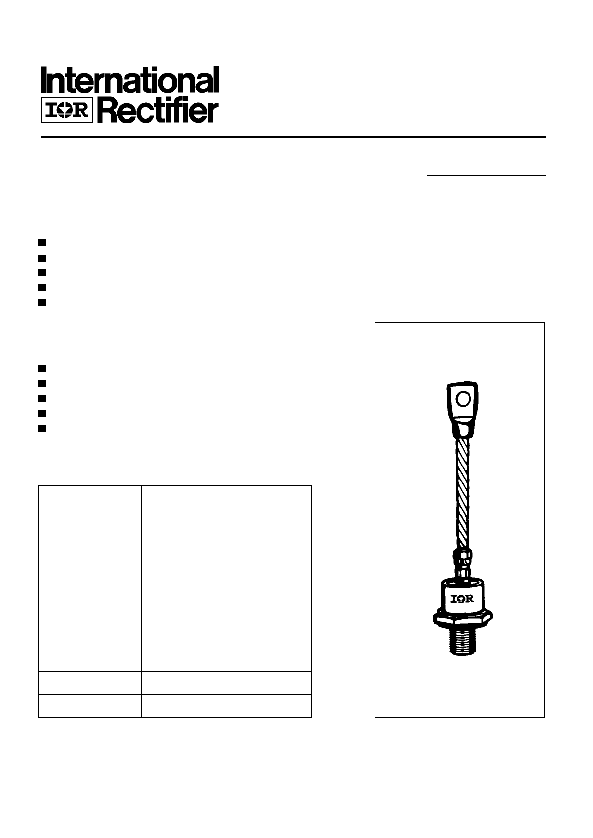
Stud V ersion
150A
Bulletin I2077/A
Features
Wide current range
High voltage ratings up to 2500V
High surge current capabilities
Stud cathode and stud anode version
Standard JEDEC types
Typical Applications
Converters
Power supplies
Machine tool controls
High power drives
Medium traction applications
Major Ratings and Characteristics
I
F(AV)
150 A
@ T
C
125 °C
I
F(RMS)
235 A
I
FSM
@
50Hz 3600 A
@ 60Hz 3770 A
I
2
t@
50Hz 65 KA
2
s
@ 60Hz 59 KA
2
s
V
RRM
range 400 to 2500 V
T
J
- 40 to 180 °C
Parameters SD150N/R Units
case style
DO-205AC (DO-30)
SD150N/R Series
ELECTRICAL SPECIFICATIONS
Voltage Ratings
Voltage V
RRM
, maximum repetitive V
RSM
, maximum non- I
RRM
max.
Type number Code peak reverse voltage repetitive peak rev. voltage @ T
J
= T
J
max.
VVmA
04 400 500
08 800 900
12 1200 1300
16 1600 1700
20 2000 2100
25 2500 2600
SD150N/R 15
I
F(AV)
Max. average forward current 150 A 180° conduction, half sine wave
@ Case temperature 125 °C
I
F(AV)
Max. average forward current 195 A 180° conduction, half sine wave
@ Case temperature 100 °C
I
F(RMS)
Max. RMS forward current 235 A DC @ 113°C case temperature
I
FSM
Max. peak, one-cycle forward, 3600 t = 10ms No voltage
non-repetitive surge current 3770 t = 8.3ms reapplied
3000 t = 10ms 100% V
RRM
3170 t = 8.3ms reapplied Sinusoidal half wave,
I
2
t Maximum I
2
t for fusing 65 t = 10ms No voltage Initial T
J
= T
J
max.
59 t = 8.3ms reapplied
46 t = 10ms 100% V
RRM
42 t = 8.3ms reapplied
I
2
√t Maximum I
2
√t for fusing 650 KA
2
√s t = 0.1 to 10ms, no voltage reapplied
V
F(TO)1
Low level value of threshold
voltage
V
F(TO)2
High level value of threshold
voltage
r
f
1
Low level value of forward
slope resistance
r
f
2
High level value of forward
slope resistance
V
FM
Max. forward voltage drop 1.5 V I
pk
= 470A, T
J
= T
J
max, t
p
= 10ms sinusoidal wave
Parameter SD150N/R Units Conditions
Forward Conduction
KA
2
s
A
V
mΩ
1.04 (I > π x I
F(AV)
),T
J
= T
J
max.
1.27 (16.7% x π x I
F(AV)
< I < π x I
F(AV)
), T
J
= T
J
max.
1.06 (I > π x I
F(AV)
),T
J
= T
J
max.
0.93 (16.7% x π x I
F(AV)
< I < π x I
F(AV)
), T
J
= T
J
max.
SD150N/R Series
T
J
Max. junction operating temperature -40 to 180
T
stg
Max. storage temperature range -55 to 200
R
thJC
Max. thermal resistance, junction to case 0.23 DC operation
R
thCS
Max. thermal resistance, case to heatsink 0.08 Mounting surface, smooth, flat and greased
T Max. allowed mounting torque ±10% 14 Nm Not lubricated threads
wt Approximate weight 120 g
Case style DO-205AC(DO-30) See Outline Table
Parameter SD150N/R Units Conditions
Thermal and Mechanical Specifications
°C
K/W
∆R
thJC
Conduction
(The following table shows the increment of thermal resistence R
thJC
when devices operate at different conduction angles than DC)
180° 0.041 0.030 T
J
= T
J
max.
120° 0.049 0.051
90° 0.063 0.068
60° 0.093 0.096
30° 0.156 0.157
Conduction angle Sinusoidal conduction Rectangular conduction Units Conditions
K/W
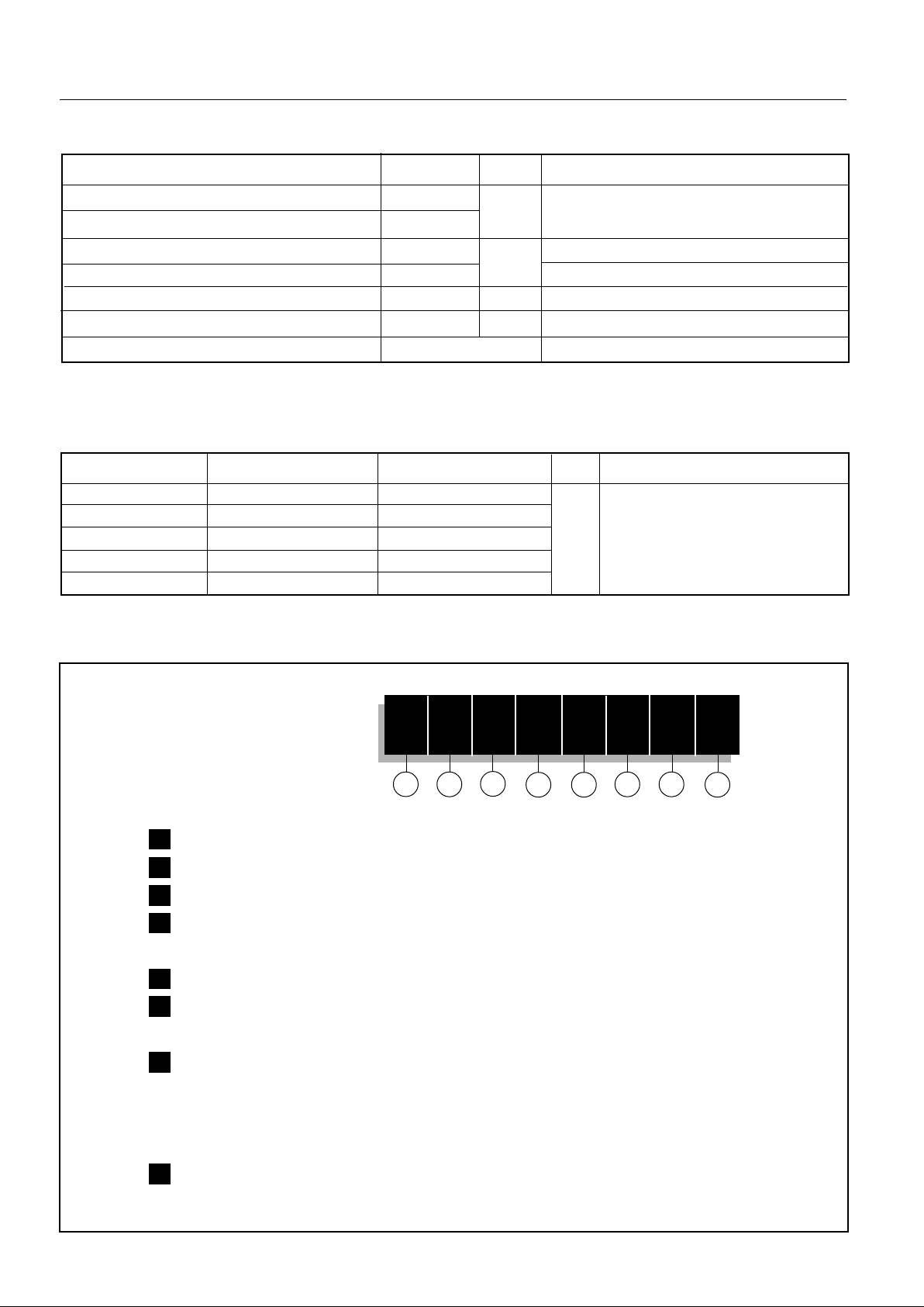
Ordering Information Table
SD 15 0 N 25 P B C
1 234 56
7
Device Code
8
1 - Diode
2 - Essential part number
3 - 0 = Standard recovery
4 - N = Stud Normal Polarity (Cathode to Stud)
R = Stud Reverse Polarity (Anode to Stud)
5 - Voltage code: Code x 100 = V
RRM
(See Voltage Ratings table)
6 - P = Stud base DO-205AC (DO-30) 1/2" 20UNF-2A
M = Stud base DO-205AC (DO-30) M12 X 1.75
7 - B = Flag top terminal (for Cathode/ Anode Leads)
S = Isolated lead with silicone sleeve
(Red = Reverse Polarity; Blue = Normal Polarity)
None = Non isolated lead
8 - C = Ceramic Housing (over 1600V)
V = Glass-metal seal (only up to 1600V)
 Loading...