


 Loading...
Fibre Channel 133 MBd and
266 MBd Transceivers in Low
Cost 1x9 Package Style
Technical Data
Features
•Full Compliance with ANSI X3T11 Fibre Channel Physical and Signaling Interface
•Multisourced 1x9 Package Style with Duplex SC Connector
•Wave Solder and Aqueous Wash Process Compatibility
•Compatible with Various Manufacturers FC-0 and FC-1 Circuits
Applications
•Fibre Channel 12.5 MB/s 12-M6-LE-I Interfaces for 1300 nm LED Links to 1500 m
•Fibre Channel 25 MB/s 25-M6-LE-I Interfaces for 1300 nm LED Links to 1500 m
Description
The HFBR-5301 and HFBR-5302 Fibre Channel Transceivers from Hewlett-Packard provide the system designer with products to implement Fibre Channel designs for use in multimode fiber (MMF) applications. These include the 12.5 MB/sec 12-M6-LE-I interface and the 25 MB/sec 25-M6-LE-I interface for 1300 nm LED links.
5963-5608E (3/95)
The products are produced in the new industry standard 1x9 SIP package style with a duplex SC connector interface as defined in the Fiber Channel ANSI FC-PH standard document.
The HFBR-5301 is a 1300 nm transceiver specified for use in 133 MBd, 12.5 MB/s, 12-M6-LE-I Fibre Channel interfaces to either 62.5/125 μm or 50/125 μm multimode fiber-optic cables.
The HFBR-5302 is a 1300 nm transceiver specified for use in 266 MBd, 25 MB/s, 25-M6-LE-I Fibre Channel interfaces to either 62.5/125 μm or 50/125 μm multimode fiber-optic cables.
Transmitter Sections
The transmitter sections of the HFBR-5301 and HFBR-5302 utilize 1300 nm InGaAsP LEDs. These LEDs are packaged in the optical subassembly portion of the transmitter section. They are driven by a custom silicon IC which converts PECL logic signals, into an analog LED drive current.
Receiver Sections
The receiver sections of the HFBR-5301 and HFBR-5302 utilize InGaAs PIN photo diodes coupled to a custom silicon transimpedance preamplifier IC.
HFBR-5301 133 MBd
HFBR-5302 266 MBd
These are packaged in the optical subassembly portion of the receiver.
These PIN/preamplifier combinations are coupled to a custom quantizer IC which provides the final pulse shaping for the logic output and the Signal Detect function. The Data output is differential. The Signal Detect output is single-ended. Both data and signal detect outputs are PECL compatible, ECL referenced (shifted) to a +5 volt power supply.
Package
The overall package concept for the HP Fibre Channel transceivers consists of three basic elements; the two optical subassemblies, an electrical subassembly and the housing with integral duplex SC connector interface. This is illustrated in the block diagram in Figure 1.
215

|
ELECTRICAL SUBASSEMBLY |
DUPLEX SC |
|
|
RECEPTACLE |
DATA OUT |
|
PIN |
|
|
|
SIGNAL |
QUANTIZER IC |
|
DETECT |
|
|
PREAMP IC |
|
|
OUT |
OPTICAL |
|
|
|
SUBASSEMBLIES |
DATA IN |
|
LED |
|
|
|
|
DRIVER IC |
|
TOP VIEW
Figure 1. Block Diagram.
The package outline drawing and pin out are shown in Figures 2 and 3. The details of this package outline and pin out are compliant with the multisource definition of the 1x9 single in-line package (SIP). The low profile of the Hewlett-Packard transceiver design complies with the
maximum height allowed for the duplex SC connector over the entire length of the package.
The optical subassemblies utilize a high volume assembly process together with low cost lens elements which result in a cost effective building block.
|
|
|
|
|
39.12 |
12.70 |
|
|
|
|
|
|
|
(1.540)MAX. |
(0.500) |
|
|
|
|
|
|
|
|
AREA |
|
|
|
|
25.40 |
MAX. |
|
RESERVED |
|
12.70 |
|
|
|
|
FOR |
|
||||
|
|
(1.000) |
|
|
PROCESS |
|
(0.500) |
|
|
|
|
|
|
|
|
|
|
|
|
|
|
|
|
PLUG |
|
|
HFBR-5XXX |
|
|
|
|
|
|
|
|
H |
|
|
|
|
|
|
|
|
DATE CODE (YYWW) |
|
|
|
|
|
|
||
SINGAPORE |
|
|
|
|
|
|
|
|
|
+ 0.08 |
|
|
|
|
|
|
|
3.30 ± 0.38 |
0.75 - 0.05 |
|
|
|
|
|
|
|
(0.030+ 0.003 ) |
10.35 |
|
|
|
|
|
||
(0.130 ± 0.015) |
MAX. |
|
|
|
|
|||
|
- 0.002 |
(0.407) |
|
|
|
|
|
|
|
|
|
2.92 |
18.52 |
|
+ 0.25 |
|
|
|
|
(0.115) |
1.27 |
|
||||
|
|
(0.729) |
|
|||||
|
|
- 0.05 |
|
|||||
|
ø |
0.46 |
(9x) |
4.14 |
(0.050+ 0.010 ) |
|
||
|
|
(0.018) |
|
(0.163) |
|
- 0.002 |
|
|
|
|
NOTE 1 |
|
|
NOTE 1 |
|
||
23.55 |
20.32 [8x(2.54/.100)] |
16.70 |
|
|
17.32 20.32 |
23.32 |
||
(0.927) |
(0.800) |
|
(0.657) |
|
|
(0.682) (0.800) (0.918) |
||
0.87
(0.034) 23.24 15.88
(0.915) (0.625)
NOTE 1: THE SOLDER POSTS AND ELECTRICAL PINS ARE PHOSPHOR BRONZE WITH TIN LEAD OVER NICKEL PLATING.
DIMENSIONS ARE IN MILLIMETERS (INCHES).
Figure 2. Package Outline Drawing.
The electrical subassembly consists of a high volume multilayer printed circuit board to which the IC chips and various surfacemount passive circuit elements are attached.
The package includes internal shields for the electrical and optical subassemblies to insure high immunity to external EMI fields and low EMI emissions.
The outer housing, including the duplex SC connector, is molded of filled non-conductive plastic to provide mechanical strength and electrical isolation. The solder posts are isolated from the circuit design of the transceiver, while they can be connected to a ground plane on the circuit board, doing so will have no impact on circuit performance.
The transceiver is attached to a printed circuit board with the nine signal pins and the two solder posts which exit the bottom of the housing. The two solder posts provide the primary mechanical strength to withstand the loads imposed on the transceiver by mating with the duplex SC connectored fiber cables.
Application Information
The Applications Engineering group in the Hewlett-Packard Optical Communication Division is available to assist with the technical understanding and design trade-offs associated with these transceivers. You can contact them through your local Hewlett-Packard sales representative.
The following information is provided to answer some of the most common questions about the use of these parts.
216
1 = VEE
2 = RD N/C
3 = RD
4 = SD
5 = VCC
6 = VCC
7 = TD
8 = TD
N/C
9 = VEE
TOP VIEW
|
8 |
|
|
|
|
dB |
7 |
|
HFBR-5301, 62.5/125µm |
|
|
– |
|
|
|
||
BUDGET |
6 |
|
|
|
|
5 |
|
|
|
|
|
HFBR-5302, 62.5/125µm |
|
|
|||
POWER |
4 |
|
HFBR-5301, |
|
|
|
|
|
|
||
3 |
|
50/125µm |
|
|
|
|
|
|
|
|
|
OPTICAL |
2 |
|
|
|
|
1 |
HFBR-5302, 50/125µm |
|
|
||
|
|
|
|
||
|
|
|
|
|
|
|
0 |
0.5 |
1 |
1.5 |
2 |
|
0 |
||||
FIBER OPTIC CABLE LENGTH – km
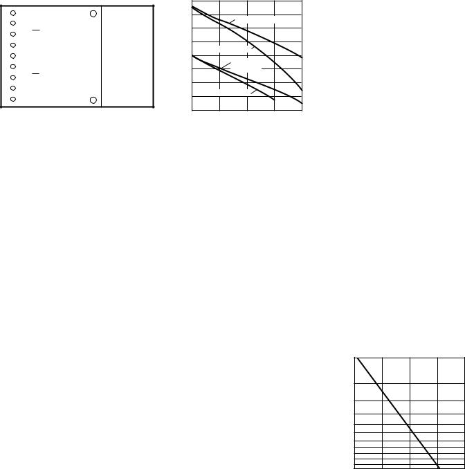
Figure 3. Pinout Diagram. |
Figure 4. Optical Power Budget vs. |
|
Fiber Optic Cable Length. |
Compatibility with Fibre Channel FC-0/1 Chip Sets
The HFBR-5301 and HFBR-5302 transceivers are compatible with various manufacturers FC-0 and FC-1 integrated circuits. Evaluation boards, which include the Hewlett-Packard transceivers, are available from these manufacturers. The Applications Engineering group in the HewlettPackard Optical Communication Division is available to assist you with implementation details.
Transceiver Optical Power Budget vs. Link Length
Optical Power Budget (OPB) is the available optical power for a fiber optic link to accommodate fiber cable losses plus losses due to in-line connectors, splices, optical switches, and to provide margin for link aging and unplanned losses due to cable plant reconfiguration or repair.
Figure 4 illustrates the predicted OPB associated with the two transceivers specified in this data sheet at the Beginning of Life (BOL). These curves represent the attenuation and chromatic plus modal dispersion losses associated with the 62.5/125 μm and 50/125 μm fiber cables only. The area under the curves
represents the remaining OPB at any link length, which is available for overcoming non-fiber cable losses.
Hewlett-Packard LED technology has produced 1300 nm LED devices with lower aging characteristics than normally associated with these technologies in the industry. The industry convention is 1.5 dB aging for 1300 nm LEDs. The HP LEDs will experience less than 1 dB of aging over normal commercial equipment mission life periods. Contact your Hewlett-Packard sales representative for additional details.
Figure 4 was generated with a Hewlett-Packard fiber optic link model containing the current industry conventions for fiber cable specifications and the Fibre Channel optical parameters. These parameters are reflected in the specified performance of the transceiver in this data sheet. This same model has been used extensively in the ANSI and IEEE committees, including the ANSI X3T9.5 committee, to establish the optical performance requirements for various fiber-optic interface standards. The cable parameters used come from the ISO/IEC JTC1/SC 25/WG3
Generic Cabling for Customer Premises per DIS 11801 document and the EIA/TIA-568-A Commercial Building Telecommunications Cabling Standard per SP-2840.
Transceiver Signaling
Operating Rate Range and
BER Performance
For purposes of definition, the symbol rate (Baud), also called signaling rate, is the reciprocal of the symbol time. Data rate (bits/ sec) is the symbol rate divided by the encoding factor used to encode the data (symbols/bit).
The specifications in this data sheet have all been measured using the standard Fibre Channel symbol rates of 133 Mbd or
266 MBd.
The transceivers may be used for other applications at signaling rates different than specified in this data sheet. Depending on the actual signaling rate, there may be some differences in optical
|
1 x 10⁻² |
|
RATE |
1 x 10⁻³ |
|
1 x 10⁻⁴ |
||
ERROR |
||
1 x 10⁻⁵ |
||
|
||
|
1 x 10⁻⁶ |
|
BIT |
1 x 10⁻⁷ |
|
1 x 10⁻⁸ |
||
|
1 x 10⁻⁹ |
1 x 10⁻¹⁰
1 x 10-11
1 x 10-12
-6 |
-4 |
-2 |
0 |
2 |
RELATIVE INPUT OPTICAL POWER – dB
CONDITIONS:
1.133 & 266 MBd
2.PRBS 27-1
3.CENTER OF SYMBOL SAMPLING
4.TA = 25 °C
5.VCC = 5 VDC
6.INPUT OPTICAL RISE/FALL TIMES = 1.0/1.9 ns
Figure 5. HFBR-5301/5302 Bit Error Rate vs. Relative Receiver Input Optical Power.
217

power budget to do this. This is primarily caused by a change of receiver sensitivity.
These transceivers can also be used for applications which require different Bit Error Rate (BER) performance. Figure 5 illustrates the typical trade-off between link BER and the receivers input optical power level.
Transceiver Jitter
Performance
The Hewlett-Packard 1300 nm transceivers are designed to operate per the system jitter allocations stated in FC-PH Annex A.4.3 and A.4.4.
The HP 1300 nm transmitters will tolerate the worst case input electrical jitter allowed, without violating the worst case output optical jitter requirements.
The HP 1300 nm receivers will tolerate the worst case input optical jitter allowed without violating the worst case output electrical jitter allowed.
The jitter specifications stated in the following tables are derived from the values in FC-PH Annex A.4.3 and A.4.4. They represent the worst case jitter contribution that the transceivers are allowed to make to the overall system jitter without violating the allowed allocation. In practice, the typical contribution of the HP transceivers is below these maximum allowed amounts.
Recommended Handling
Precautions
Hewlett-Packard recommends that normal static precautions be taken in handling and assembly of these transceivers to prevent damage and/or degradation which
may be induced by electrostatic discharge (ESD). These transceivers are certified as MIL-STD- 883C Method 3015.4 Class 2 devices.
Care should be used to avoid shorting the receiver data or signal detect outputs directly to ground.
Solder and Wash Process
Compatibility
The transceivers are delivered with a protective process plug inserted into the duplex SC connector receptacle. This process plug protects the optical subassemblies during wave solder and aqueous wash processing and acts as a dust cover during shipping.
These transceivers are compatible with industry standard wave and hand solder processes.
Shipping Container
The transceiver is packaged in a shipping container designed to protect it from mechanical and ESD damage during shipment or storage.
Board Layout – Decoupling
Circuit and Ground Planes
You should take care in the layout of your circuit board to achieve optimum performance from these transceivers. Figure 6 provides a good example of a schematic for a power supply decoupling circuit that works well with these parts. Hewlett-Packard further recommends that a contiguous ground
NO INTERNAL CONNECTION |
|
NO INTERNAL CONNECTION |
|||||||||
|
|
|
|
|
|
HFBR-530X |
|
|
|
|
|
|
|
|
|
|
|
TOP VIEW |
|
|
|
|
|
Rx |
|
|
|
|
|
Rx |
Tx |
|
|
|
Tx |
VEE |
RD |
RD |
SD |
VCC |
VCC |
TD |
TD |
VEE |
|||
1 |
2 |
3 |
|
4 |
5 |
6 |
7 |
|
8 |
9 |
|
|
|
|
C1 |
|
|
C2 |
|
|
|
|
|
|
|
VCC |
|
TERMINATION |
|
|
|
L1 |
L2 |
R2 |
R3 |
|
|
|
|
|
|
|
|
AT PHY |
|
|
|
|
|
R1 |
R4 |
DEVICE |
|
VCC |
C3 |
|
C4 |
||
INPUTS |
R5 |
R7 |
VCC FILTER |
|
C5 |
||
|
|
|
|||||
|
|
|
AT VCC PINS |
|
|
||
|
|
|
TRANSCEIVER |
|
|||
|
|
C6 |
R9 |
|
|
TERMINATION |
|
R6 |
|
|
|
AT TRANSCEIVER |
|||
|
R8 |
|
|
|
|||
|
|
|
R10 |
|
|
INPUTS |
|
|
|
|
|
|
|
|
|
|
RD |
RD |
SD |
VCC |
|
TD |
TD |
NOTES:
THE SPLIT-LOAD TERMINATIONS FOR ECL SIGNALS NEED TO BE LOCATED AT THE INPUT OF DEVICES RECEIVING THOSE ECL SIGNALS. RECOMMEND 4-LAYER PRINTED CIRCUIT BOARD WITH 50 OHM MICROSTRIP SIGNAL PATHS BE USED.
R1 = R4 = R6 = R8 = R10 = 130 ohms.
R2 = R3 = R5 = R7 = R9 = 82 ohms.
C1 = C2 = C3 = C5 = C6 = 0.1 µF.
C4 = 10 µF.
L1 = L2 = 1 µH COIL OR FERRITE INDUCTOR.
Figure 6. Recommended Decoupling and Termination Circuits.
218
Loading...