


 Loading...
HP HFBR-5205T, HFBR-5205, HFBR-5204T, HFBR-5204, HFBR-5203T Datasheet
...ATM Multimode Fiber Transceivers
for SONET OC-3/SDH STM-1 in Low Cost 1x9 Package Style
Technical Data
HFBR-5203/-5203T 800 nm 300 m HFBR-5204/-5204T 1300 nm 500 m HFBR-5205/-5205T 1300 nm 2 km
Features
•Full Compliance with ATM Forum UNI SONET OC-3 Multimode Fiber Physical Layer Specification
•Multisourced 1 x 9 Package Style with Choice of Duplex SC or Duplex ST* Receptacle
•Wave Solder and Aqueous Wash Process Compatibility
•Manufactured in an ISO 9002 Certified Facility
Applications
•Multimode Fiber ATM Backbone Links
•Multimode Fiber ATM Wiring Closet to Desktop Links
•Very Low Cost Multimode Fiber 800 nm ATM Wiring Closet to Desktop Links
•ATM 155 Mbps/194 MBd Encoded Links (available upon special request)
Description
The HFBR-5200 family of transceivers from Hewlett-Packard provide the system designer with products to implement a range of solutions for multimode fiber SONET OC-3 (SDH STM-1)
physical layers for ATM and other services.
These transceivers are all supplied in the new industry standard 1x9 SIP package style with either a duplex SC or a duplex ST* connector interface.
ATM 2000 m Backbone Links
The HFBR-5205/-5205T are 1300 nm products with optical performance compliant with the SONET STS-3c (OC-3) Physical Layer Interface Specification. This physical layer is defined in the ATM Forum User-Network Interface (UNI) Specification Version 3.0. This document references the ANSI T1E1.2 specification for the details of the interface for 2000 meter multimode fiber backbone links.
Selected versions of these transceivers may be used to implement the ATM Forum UNI Physical Layer Interface at the 155 Mbps/194 MBd rate.
The ATM 100 Mbps/125 MBd Physical Layer interface is best implemented with the HFBR-5100 family of FDDI Transceivers which are specified for use in this 4B/5B encoded physical layer per the FDDI PMD standard.
*ST is a registered trademark of AT&T Lightguide Cable Connectors.
ATM 500 m Backbone and Desktop Links
The HFBR-5204/-5204T are 1300 nm products which are similar to the HFBR-5205/5205T except that they are intended to provide a lower cost SONET OC-3 link to distances up to 500 meters in 62.5/125 μm multimode fiber optic cables.
Very Low Cost ATM 300 m Desktop Links
The HFBR-5203/-5203T are very low cost 800 nm alternatives to the HFBR-5204/-5204T for SONET OC-3 links to distances up to 300 meters in 62.5/125 μm multimode fiber optic cables.
Transmitter Sections
The transmitter sections of the HFBR-5204 and HFBR-5205 series utilize 1300 nm InGaAsP LEDs and the HFBR-5203 series
5965-9729E (5/97) |
107 |
uses a low cost 800 nm AlGaAs LED. These LEDs are packaged in the optical subassembly portion of the transmitter section. They are driven by a custom silicon IC which converts differential PECL logic signals, ECL referenced (shifted) to a +5 Volt supply, into an analog LED drive current.
Receiver Sections
The receiver sections of the HFBR-5204 and HFBR-5205 series utilize InGaAs PIN photodiodes coupled to a custom silicon transimpedance preamplifier IC. The HFBR-5203 series uses the same preamplifier IC in conjunction with an inexpensive silicon PIN photodiode. These are packaged in the optical subassembly portion of the receiver.
These PIN/preamplifier combinations are coupled to a custom quantizer IC which provides the final pulse shaping for the logic output and the Signal Detect function. The data output is differential. The signal detect output is single-ended. Both data and signal detect outputs are PECL compatible, ECL referenced (shifted) to a +5 volt power supply.
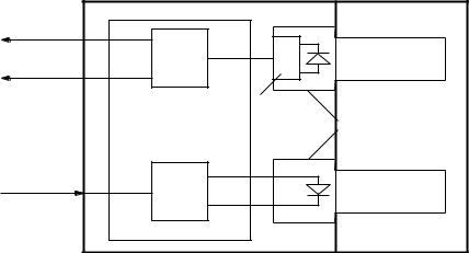
Package
The overall package concept for the HP transceivers consists of three basic elements; the two optical subassemblies, an electrical subassembly, and the housing as illustrated in the block diagrams in Figure 1 and
Figure 1a.
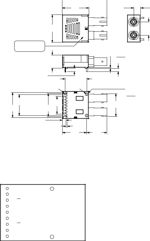
The package outline drawing and pin out are shown in Figures 2, 2a, and 3. The details of this package outline and pin out are compliant with the multisource definition of the 1x9 SIP. The low profile of the Hewlett-Packard
transceiver design complies with the maximum height allowed for the duplex SC connector over the entire length of the package.
The optical subassemblies utilize a high volume assembly process together with low cost lens elements which result in a cost effective building block.
The electrical subassembly consists of a high volume multilayer printed circuit board on which the IC chips and various surfacemounted passive circuit elements are attached.
The package includes internal shields for the electrical and optical subassemblies to insure low EMI emissions and high immunity to external EMI fields.
connection to a ground plane on the circuit board.
The transceiver is attached to a printed circuit board with the nine signal pins and the two solder posts which exit the bottom of the housing. The two solder posts provide the primary mechanical strength to withstand the loads imposed on the transceiver by mating with the duplex or simplex SC or ST connectored fiber cables.
Note: The “T” in the product numbers indicates a transceiver with a duplex ST connector receptacle. Product numbers without a “T” indicate transceivers with a duplex SC connector receptacle.
The outer housing including the duplex SC connector or the duplex ST ports is molded of filled non-conductive plastic to provide mechanical strength and electrical isolation. The solder posts of the Hewlett-Packard design are isolated from the circuit design of the transceiver and do not require
Application Information
The Applications Engineering group in the Hewlett-Packard Optical Communication Division is available to assist you with the technical understanding and design trade-offs associated with these transceivers. You can contact them through your HewlettPackard sales representative.
|
ELECTRICAL SUBASSEMBLY |
DUPLEX SC |
DIFFERENTIAL |
|
RECEPTACLE |
|
|
|
DATA OUT |
|
PIN PHOTODIODE |
SINGLE-ENDED |
|
|
|
|
|
SIGNAL |
QUANTIZER IC |
|
DETECT OUT |
|
|
PREAMP IC |
|
|
|
|
OPTICAL |
|
|
SUBASSEMBLIES |
DIFFERENTIAL |
|
LED |
DATA IN |
|
|
|
|
|
|
DRIVER IC |
|
TOP VIEW
Figure 1. Block Diagram.
108

|
ELECTRICAL SUBASSEMBLY |
DUPLEX ST |
DIFFERENTIAL |
|
RECEPTACLE |
|
|
|
DATA OUT |
|
PIN PHOTODIODE |
SINGLE-ENDED |
|
|
|
|
|
SIGNAL |
QUANTIZER IC |
|
DETECT OUT |
|
|
PREAMP IC |
|
|
|
|
OPTICAL |
|
|
SUBASSEMBLIES |
DIFFERENTIAL |
|
LED |
DATA IN |
|
|
|
|
|
|
DRIVER IC |
|
|
TOP VIEW |
|
Figure 1a. ST Block Diagram.
|
|
|
|
39.12 |
12.70 |
|
|
|
|
|
(1.540)MAX. |
(0.500) |
|
|
|
|
|
|
AREA |
|
|
|
|
25.40 |
|
RESERVED |
12.70 |
|
|
|
|
|
||
|
|
(1.000)MAX. |
|
FOR |
(0.500) |
|
|
|
|
|
|
PROCESS |
|
|
|
|
|
|
PLUG |
|
HFBR |
|
|
|
|
||
|
-5XXX |
|
|
|
|
|
DATE CODE (YYWW) |
|
|
|
|
||
SINGAPORE |
|
|
|
|
|
|
|
+ 0.08 |
|
|
|
|
|
3.30 ± 0.38 |
0.75 - 0.05 |
|
|
|
|
|
+ 0.003 |
|
10.35 |
|
|
|
|
|
|
|
|
|
||
(0.130 ± 0.015) |
(0.030 - 0.002) |
(0.407)MAX. |
|
|
|
|
|
|
|
2.92 |
18.52 |
|
+ 0.25 |
|
|
|
(0.115) |
1.27 |
||
|
|
|
(0.729) |
|||
|
|
|
- 0.05 |
|||
|
|
0.46 |
4.14 |
|
+ 0.010 |
|
|
ø |
(0.018)(9x) |
(0.163) |
(0.050 |
- 0.002) |
|
|
|
NOTE 1 |
|
NOTE 1 |
||
23.55 |
20.32 [8x(2.54/.100)] |
16.70 |
|
|
17.32 20.32 23.32 |
|
(0.927) |
(0.800) |
|
(0.657) |
|
|
(0.682) (0.800) (0.918) |
0.87
(0.034) 23.24 15.88
(0.915) (0.625)
NOTE 1: THE SOLDER POSTS AND ELECTRICAL PINS ARE PHOSPHOR BRONZE WITH TIN LEAD OVER NICKEL PLATING.
DIMENSIONS ARE IN MILLIMETERS (INCHES).
Figure 2. Package Outline Drawing.
109
(1.000)25.4 MAX.
HFBR-5103T
DATE CODE (YYWW)
SINGAPORE
(0.471)12.0 MAX.
 42 MAX.
  (1.654)
24.8 |
5.99 |
|
(0.236) |
||
(0.976) |
||
|
12.7
(0.500)
0.5 |
+ 0.08 |
|
- 0.05 |
|
|
(0.020) |
|
|
+ 0.003 |
( |
|
(- 0.002 |
||
|
3.2 |
|
|
|
|
|
(0.126) |
|
20.32 ± 0.38 |
3.3 ± 0.38 |
|
|
φ 0.46 |
||||
|
|
(± 0.015) |
(0.130) (± 0.015) |
||
|
(0.022) |
φ |
2.6 |
+ 0.25 |
|
|
NOTE 1 |
||||
|
(0.102) |
- 0.05 |
|||
|
|
|
|||
|
|
|
|
|
|
20.32 |
|
|
|
|
(+- 0.0020.010 |
|
17.4 |
|
|
|
|
(0.800)[(8x (2.54/0.100)] |
|
|
20.32 |
||
22.86 |
21.4 |
(0.685) |
|
|
(0.800) |
(0.900) |
(0.843) |
|
|
|
|
3.6 |
|
|
(0.142) |
1.3 |
|
|
|
|
|
(0.051) |
|
|
23.38 |
18.62 |
|
(0.921) |
(0.733) |
(
NOTE 1: PHOSPHOR BRONZE IS THE BASE MATERIAL FOR THE POSTS & PINS WITH TIN LEAD OVER NICKEL PLATING.
DIMENSIONS IN MILLIMETERS (INCHES).
Figure 2a. ST Package Outline Drawing.
1 = VEE
N/C
2 = RD
3 = RD
4 = SD
5 = VCC
6 = VCC
7 = TD
8 = TD
N/C
9 = VEE
TOP VIEW
Figure 3. Pin Out Diagram.
110
The following information is provided to answer some of the most common questions about the use of these parts.
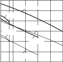
Transceiver Optical Power Budget versus Link Length
Optical Power Budget (OPB) is the available optical power for a fiber optic link to accommodate fiber cable losses plus losses due to in-line connectors, splices, optical switches, and to provide margin for link aging and unplanned losses due to cable plant reconfiguration or repair.
Figure 4 illustrates the predicted OPB associated with the three transceivers series specified in this data sheet at the Beginning of Life (BOL). These curves represent the attenuation and chromatic plus modal dispersion losses associated with the 62.5/125 μm and 50/125 μm fiber cables only. The area under the curves represents the remaining OPB at any link length, which is available for overcoming non-fiber cable losses.
Hewlett-Packard LED technology has produced 800 nm LED and 1300 nm LED devices with lower aging characteristics than normally associated with these technologies in the industry. The industry convention is 3 dB aging for 800 nm and 1.5 dB aging for 1300 nm LEDs. The 1300 nm HP LEDs are specified to experience less than 1 dB of aging over normal commercial equipment mission life periods. Contact your Hewlett-Packard sales representative for additional details.
Figure 4 was generated for the 1300 nm transceivers with a Hewlett-Packard fiber optic link model containing the current industry conventions for fiber cable specifications and the draft ANSI T1E1.2. These optical parameters are reflected in the guaranteed performance of the transceiver specifications in this data sheet. This same model has been used extensively in the ANSI and IEEE committees, including the ANSI T1E1.2 committee, to establish the optical performance requirements for various fiber
|
12 |
|
|
|
|
10 |
|
HFBR-5205, 62.5/125 µm |
|
(dB) |
|
|
||
|
HFBR-5203, |
|||
|
62.5/125 µm |
|||
BUDGET |
|
|||
8 |
|
|
||
|
|
HFBR-5205, |
||
|
|
50/125 µm |
||
POWER |
6 |
HFBR-5203, |
||
|
||||
|
50/125 µm |
|
||
4 |
|
HFBR-5204, |
||
OPTICAL |
|
|||
|
62.5/125 µm |
|||
|
|
|||
2 |
|
HFBR-5204, |
||
|
|
|
||
|
|
|
50/125 µm |
|
0 |
0.5 |
1.0 |
1.5 |
2.0 |
2.5 |
0.3 |
FIBER OPTIC CABLE LENGTH (km)
Figure 4. Optical Power Budget vs. Fiber Optic Cable Length.
optic interface standards. The cable parameters used come from the ISO/IEC JTC1/SC 25/WG3 Generic Cabling for Customer Premises per DIS 11801 document and the EIA/TIA-568-A Commercial Building Telecommunications Cabling Standard per SP-2840.
The HFBR-5203 series 800 nm transceiver curve in Figure 4 was generated based on extensive empirical test data of the 800 nm transceiver performance. The curve includes the effect of typical fiber attenuation, plus receiver sensitivity loss due to chromatic and metal dispersion losses through the fiber.
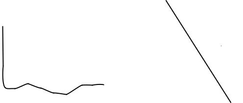
Transceiver Signaling Operating Rate Range and BER Performance
For purposes of definition, the symbol (Baud) rate, also called signaling rate, is the reciprocal of the symbol time. Data rate (bits/ sec) is the symbol rate divided by the encoding factor used to encode the data (symbols/bit).
When used in 155 Mbps SONET OC-3 applications the performance of the 1300 nm transceivers, HFBR-5204/5205 is guaranteed to the full conditions listed in individual product specification tables.
The transceivers may be used for other applications at signaling rates different than 155 Mbps with some variation in the link optical power budget. Figure 5 gives an indication of the typical performance of these products at different rates.
These transceivers can also be used for applications which require different Bit Error Rate (BER) performance. Figure 6
111
BUDGET |
|
2.5 |
|
|
|
|
|
|
|
|
|
|
|
|
|
|
|
|
|
OPTICALRELATIVETRANSCEIVERPOWER |
BERCONSTANTAT(dB) |
2.0 |
|
|
|
|
|
|
|
|
|
|
|
|
|
|
|
|
|
|
|
|
|
|
|
|
|
|
|
|
|
|
|
|
|
|
|||
1.5 |
|
|
|
|
|
|
|
|
|
|
|
|
|
|
|
|
|
||
|
|
|
|
|
|
|
|
|
|
|
|
|
|
|
|
|
|
|
|
|
|
1.0 |
|
|
|
|
|
|
|
|
|
|
|
|
|
|
|
|
|
|
|
|
|
|
|
|
|
|
|
|
|
|
|
|
|
|
|
|
|
|
|
0.5 |
|
|
|
|
|
|
|
|
|
|
|
|
|
|
|
|
|
|
|
|
|
|
|
|
|
|
|
|
|
|
|
|
|
|
|
|
|
|
|
0 |
|
|
|
|
|
|
|
|
|
|
|
|
|
|
|
|
|
|
|
|
|
|
|
|
|
|
|
|
|
|
|
|
|
|
|
|
|
|
|
0.5 |
|
|
|
|
|
|
|
|
|
|
|
|
|
|
|
|
|
|
|
0 |
25 |
50 |
75 |
100 |
125 |
150 |
175 |
200 |
|||||||||
SIGNAL RATE (MBd)
CONDITIONS:
1.PRBS 27-1
2.DATA SAMPLED AT CENTER OF DATA SYMBOL.
3.BER = 10-6
4.TA = 25° C
5.VCC = 5 Vdc
6.INPUT OPTICAL RISE/FALL TIMES = 1.0/2.1 ns.
Figure 5. Transceiver Relative Optical Power Budget at Constant BER vs. Signaling Rate.
|
1 x 10⁻² |
|
|
|
|
|
|
|
|
|
|
|
|
|
|
|
|
|
|
|
|
|
|
|
|
|
|
|
|
|
|
RATE |
1 x 10⁻³ |
|
|
|
|
|
|
|
|
|
|
|
|
|
|
|
|
|
|
|
|
|
|
|
|
|
|
|
|
||
1 x 10⁻⁴ |
|
|
|
|
|
|
|
|
|
|
|
|
|
|
|
|
|
|
|
HFBR-5203/5204/5205 |
|
|
|||||||||
ERROR |
1 x 10⁻⁵ |
|
|
|
|
|
|
|
SERIES |
|
|
|
|
|
|
|
|
|
|
|
|
|
|
|
|
|
|
|
|
|
|
|
1 x 10⁻⁶ |
|
|
|
|
|
|
|
|
|
|
|
|
|
|
|
|
|
|
|
|
|
|
|
|
|
|
SYMBOL |
|
||
BIT |
1 x 10⁻⁷ |
|
|
|
|
|
|
CENTER OF |
|
||||||
|
|
|
|
|
|
|
|
|
|
|
|
|
|
|
|
|
1 x 10⁻⁸ |
|
|
|
|
|
|
|
|
|
|
|
|
|
|
|
|
|
|
|
|
|
|
|
|
|
|
|
|
|
|
|
1 x 10⁻⁹ |
|
|
|
|
|
|
|
|
|
|
|
|
|
|
|
|
|
|
|
|
|
|
|
|
|
|
|
|
|
|
|
1 x 10⁻¹⁰ |
|
|
|
|
|
|
|
|
|
|
|
|
|
|
|
|
|
|
|
|
|
|
|
|
|
|
|
|
|
|
|
1 x 10-11 |
|
|
|
|
|
|
|
|
|
|
|
|
|
|
|
|
|
|
|
|
|
|
|
|
|
|
|
|
|
|
|
1 x 10-12 |
|
|
|
|
|
|
|
|
|
|
|
|
|
|
|
|
|
|
|
|
|
|
|
|
|
|
|
|
|
|
|
-6 |
-4 |
-2 |
0 |
2 |
|
4 |
||||||||
|
|
|
RELATIVE INPUT OPTICAL POWER – dB |
|
|||||||||||
CONDITIONS:
1.155 MBd
2.PRBS 27-1
3.CENTER OF SYMBOL SAMPLING.
4.TA = 25° C
5.VCC = 5 Vdc
6.INPUT OPTICAL RISE/FALL TIMES = 1.0/2.1 ns.
Figure 6. Bit Error Rate vs. Relative Receiver Input Optical Power.
illustrates the typical trade-off between link BER and the receivers input optical power level.
Transceiver Jitter Performance
The Hewlett-Packard 1300 nm transceivers are designed to operate per the system jitter allocations stated in Table B1 of Annex B of the draft ANSI T1E1.2 Revision 3 standard.
The HP 1300 nm transmitters will tolerate the worst case input electrical jitter allowed in Annex B without violating the worst case output optical jitter requirements.
The HP 1300 nm receivers will tolerate the worst case input optical jitter allowed in Annex B
without violating the worst case output electrical jitter allowed.
The jitter specifications stated in the following 1300 nm transceiver specification tables are derived from the values in Table B1 of Annex B. They represent the worst case jitter contribution that the transceivers are allowed to make to the overall system jitter without violating the Annex B allocation example. In practice, the typical contribution of the HP transceivers is well below these maximum allowed amounts.
Recommended Handling Precautions
Hewlett-Packard recommends that normal static precautions be taken in the handling and assembly of these transceivers to prevent damage which may be induced by electrostatic discharge
(ESD). The HFBR-5200 series of transceivers meet MIL-STD-883C Method 3015.4 Class 2 products.
Care should be used to avoid shorting the receiver data or signal detect outputs directly to ground without proper current limiting impedance.
Solder and Wash Process Compatibility
The transceivers are delivered with protective process plugs inserted into the duplex SC or duplex ST connector receptacle. This process plug protects the optical subassemblies during wave solder and aqueous wash processing and acts as a dust cover during shipping.
These transceivers are compatible with either industry standard wave or hand solder processes.
112
Loading...