


HCPL-530K
HP HCPL-530K, HCPL-5301, HCPL-5300, 5962-9685201HYC, 5962-9685201HYA Datasheet
...
1-498
H
Intelligent Power Module
and Gate Drive Interface
Optocouplers
Technical Data
Applications
• Military and Space
• High Reliability Systems
• Harsh Industrial
Environments
• Transportation, Medical, and
Life Critical Systems
• IPM Isolation
• Isolated IGBT/MOSFET Gate
Drive
• AC and Brushless DC Motor
Drives
• Industrial Inverters
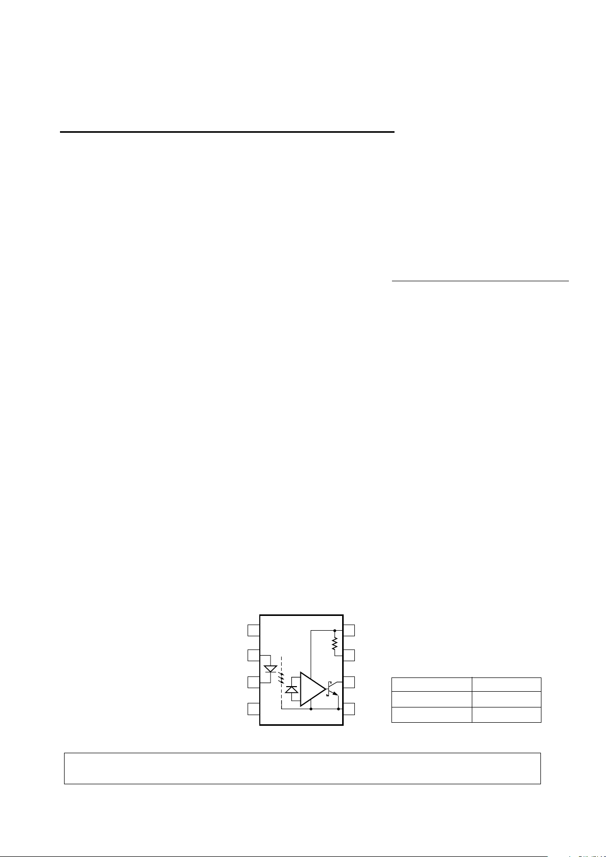
Description
The HCPL-5300/5301 devices
consist of a GaAsP LED optically
coupled to an integrated high
gain photo detector in a
hermetically sealed package. The
The connection of a 0.1
µ
F bypass capacitor between pins 5 and 8 is recommended.
products are capable of operation
and storage over the full military
temperature range and can be
purchased as either standard
product or with full MIL-PRF-
38534 Class Level H or K testing
or from the DESC Drawing 5962-
96852. All devices are
manufactured and tested on a
MIL-PRF-38534 certified line and
are included in the DESC
Qualified Manufacturers List
QML-38534 for Hybrid Micro-
circuits. Minimized propagation
delay difference between devices
make these optocouplers excellent
solutions for improving inverter
efficiency through reduced
switching dead time. An on chip
20 kΩ output pull-up resistor can
be enabled by shorting output
pins 6 and 7, thus eliminating the
need for an external pull-up
resistor in common IPM applica-
tions. Specifications and
performance plots are given for
typical IPM applications.
HCPL-5300
HCPL-5301
5962-96852
CAUTION: It is advised that normal static precautions be taken in handling and assembly of this component to
prevent damage and/or degradation which may be induced by ESD.
Features
• Performance Specified Over
Full Military Temperature
Range: -55°C to 125°C
• Fast Maximum Propagation
Delays
t
PHL
= 450 ns,
t
PLH
= 650 ns
• Minimized Pulse Width
Distortion (PWD = 450 ns)
• High Common Mode
Rejection (CMR): 10 kV/µs at
V
CM
= 1000 V
• CTR > 30% at I
F
= 10 mA
• 1500 Vdc Withstand Test
Voltage
• Manufactured and Tested on
a MIL-PRF-38534 Certified
Line
• Hermetically Sealed
Packages
• Dual Marked with Device
Part Number and DESC
Drawing Number
• QML-38534, Class H and K
• HCPL-4506 Function
Compatibility
8
7
6
1
3
SHIELD
5
2
4
20 kΩ
Schematic Diagram
Truth Table
LED V
O
ON L
OFF H
5964-9648E
1-499
Selection Guide-Package Styles and Lead
Configuration Options
HP Part # and Options
Commercial HCPL-5300
MIL-PRF-38534, Class H HCPL-5301
MIL-PRF-38534, Class K HCPL-530K
Standard Lead Finish Gold Plate
Solder Dipped Option #200
Butt Cut/Gold Plate Option #100
Gull Wing/Soldered Option #300
SMD Part #
Prescript for all below 5962-
Either Gold or Solder 9685201HPX
Gold Plate 9685201HPC
Solder Dipped 9685201HPA
Butt Cut/Gold Plate 9685201HYC
Butt Cut/Soldered 9685201HYA
Gull Wing/Soldered 9685201HXA
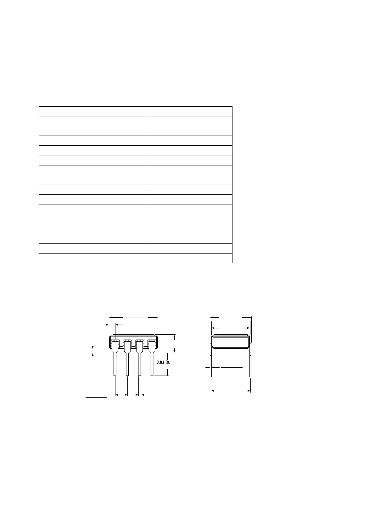
Outline Drawing
3.81 (0.150)
MIN.
4.32 (0.170)
MAX.
9.40 (0.370)
9.91 (0.390)
0.51 (0.020)
MAX.
2.29 (0.090)
2.79 (0.110)
0.51 (0.020)
MIN.
0.76 (0.030)
1.27 (0.050)
8.13 (0.320)
MAX.
7.36 (0.290)
7.87 (0.310)
0.20 (0.008)
0.33 (0.013)
7.16 (0.282)
7.57 (0.298)
NOTE: DIMENSIONS IN MILLIMETERS (INCHES).
1-500
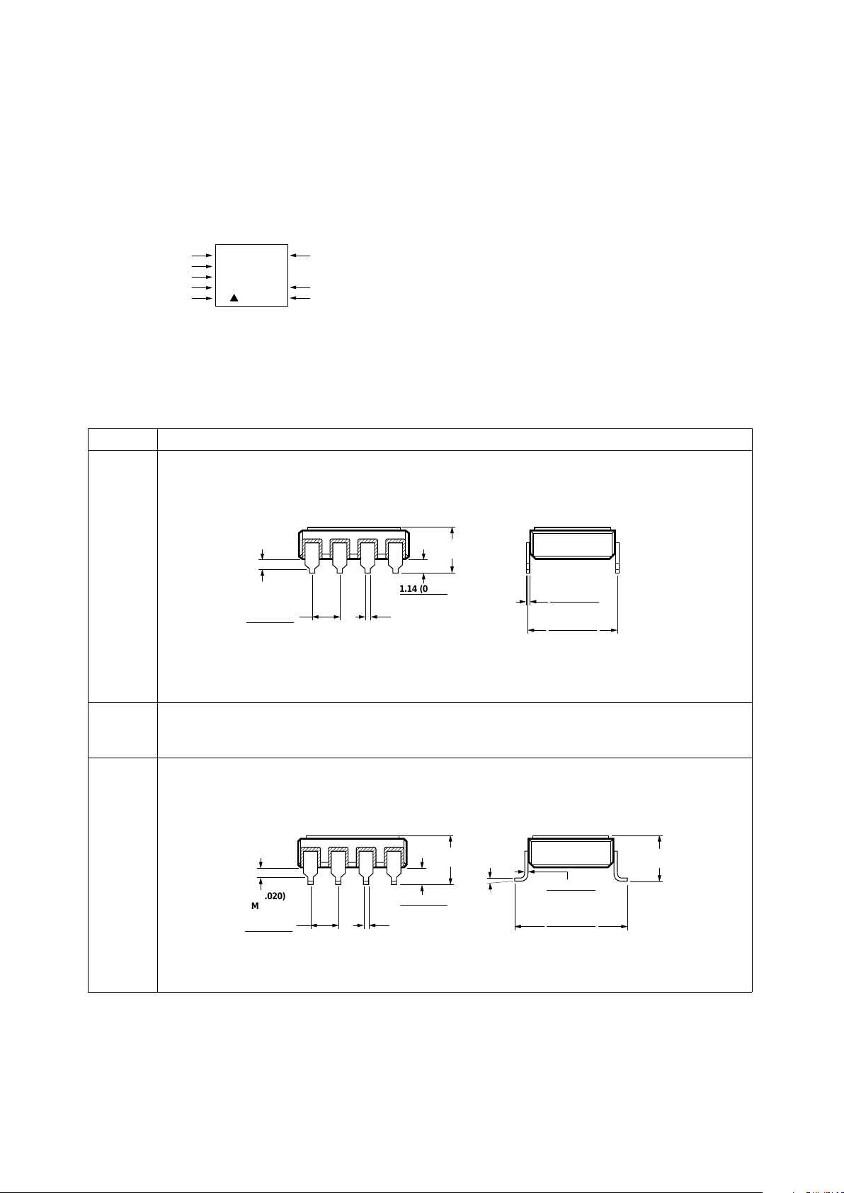
Device Marking
Hermetic Optocoupler Options
Option Description
100 Surface mountable hermetic optocoupler with leads trimmed for butt joint assembly. This
option is available on commercial and hi-rel product in 8 pin DIP (see drawings below for
details).
200 Lead finish is solder dipped rather than gold plated. This option is available on commercial
and hi-rel product in 8 pin DIP. DESC Drawing part numbers contain provisions for lead
finish.
300 Surface mountable hermetic optocoupler with leads cut and bent for gull wing assembly.
This option is available on commercial and hi-rel product in 8 pin DIP (see drawings below
for details). This option has solder dipped leads.
1.14 (0.045)
1.40 (0.055)
4.32 (0.170)
MAX.
0.51 (0.020)
MAX.
2.29 (0.090)
2.79 (0.110)
0.51 (0.020)
MIN.
7.36 (0.290)
7.87 (0.310)
0.20 (0.008)
0.33 (0.013)
NOTE: DIMENSIONS IN MILLIMETERS (INCHES).
COMPLIANCE INDICATOR,*
DATE CODE, SUFFIX (IF NEEDED)
HP QYYWWZ
XXXXXX
XXXXXXX
XXX USA
50434
COUNTRY OF MFR.
HP FSCN*
HP LOGO
DESC SMD*
PIN ONE/
ESD IDENT
HP P/N
DESC SMD*
* QUALIFIED PARTS ONLY
0.51 (0.020)
MIN.
5.57 (0.180)
MAX.
0.51 (0.020)
MAX.
2.29 (0.090)
2.79 (0.110)
1.40 (0.055)
1.65 (0.065)
9.65 (0.380)
9.91 (0.390)
5° MAX.
5.57 (0.180)
MAX.
0.20 (0.008)
0.33 (0.013)
NOTE: DIMENSIONS IN MILLIMETERS (INCHES).

1-501
Absolute Maximum Ratings
Storage Temperature (T
S
) ............................................................................................................. -65 to 150°C
Operating Temperature (T
A
) ......................................................................................................... -55 to 125°C
Junction Temperature (T
J
) ...................................................................................................................... 175°C
Average Input Current (I
F(AVG)
) ............................................................................................................... 25 mA
Peak Input Current (50% duty cycle, ≤ 1 ms pulse width) (I
F(PEAK)
) ........................................................ 50 mA
Peak Transient Input Current (<1 µs pulse width, 300 pps) (I
F(TRAN)
) ..................................................... 1.0 A
Reverse Input Voltage (Pin 3-2) (V
R
)............................................................................................................ 5 V
Average Output Current (Pin 6) (I
O(AVG)
) ................................................................................................ 15 mA
Resistor Voltage (Pin 7) (V
7
) ......................................................................................................... -0.5 V to V
CC
Output Voltage (Pin 6-5) (V
O
) ........................................................................................................ -0.5 to 30 V
Supply Voltage (Pin 8-5) (V
CC
) ....................................................................................................... -0.5 to 30 V
Output Power Dissipation (P
O
)............................................................................................................. 100 mW
Total Power Dissipation (P
T
)................................................................................................................ 145 mW
Lead Solder Temperature (soldering, 10 seconds) .................................................................................. 260°C
ESD Classification
(MIL-STD-883, Method 3015)
HCPL-5300/5301 ......................(∆),Class 1
Recommended Operating Conditions
Parameter Symbol Min. Max. Units
Power Supply Voltage V
CC
4.5 30 Volts
Output Voltage V
O
0 30 Volts
Input Current (ON) I
F(ON)
10 20 mA
Input Voltage (OFF) V
F(OFF)
-5 0.8 V

1-502
Electrical Specifications
Over recommended operating conditions (T
A
= -55°C to +125°C, V
CC
= +4.5 V to 30 V,
I
F(ON)
= 10 mA to 20 mA, V
F(OFF)
= -5 V to 0.8 V) unless otherwise specified.
Group A
Sub-
Parameter Symbol groups
[12]
Min. Typ.* Max. Units Test Conditions Fig. Note
Current Transfer CTR 1, 2, 3 30 90 % I
F
= 10 mA, V
O
= 0.6 V 1
Ratio
Low Level Output I
OL
1, 2, 3 3.0 9.0 mA I
F
= 10 mA, V
O
= 0.6 V 1, 2
Current
Low Level Output V
OL
1, 2, 3 0.3 0.6 V I
O
= 2.4 mA
Input Threshold I
TH
1, 2, 3 1.5 5.0 mA V
O
= 0.8 V, 1 7
Current I
O
= 0.75 mA
High Level I
OH
1, 2, 3 5 75 µAV
F
= 0.8 V 3
Output Current
High Level Supply I
CCH
1, 2, 3 0.6 1.5 mA V
F
= 0.8 V, V
O
= Open 7
Current
Low Level Supply I
CCL
1, 2, 3 0.6 1.5 mA I
F
= 10 mA, V
O
= Open 7
Current
Input Forward V
F
1, 2, 3 1.0 1.5 1.8 V I
F
= 10 mA 4
Voltage
Temperature ∆V
F
/ -1.6 mV/°CI
F
= 10 mA
Coefficient of ∆T
A
Forward Voltage
Input Reverse BV
R
1, 2, 3 5 V I
R
= 100 µA
Breakdown Voltage
Input Capacitance C
IN
90 pF f = 1 MHz, V
F
= 0 V
Input-Output I
I-O
1 1.0 µA RH = 45%, t = 5 sec, 2
Insulation Leakage V
I-O
= 1500 Vdc,
Current T
A
= 25° C
Resistance R
I-O
10
12
Ω V
I-O
= 500 Vdc 2
(Input-Output)
Capacitance C
I-O
2.4 pF f = 1 MHz 2
(Input-Output)
Internal Pull-up R
L
1 142028kΩT
A
= 25° C 4, 5,
Resistor 6
Internal Pull-up ∆R
L
/ 0.014 kΩ/°C
Resistor ∆T
A
Temperature
Coefficient
*All typical values at 25°C, V
CC
= 15 V.
Voltage
 Loading...