


 Loading...
H
Isolated 15-bit A/D Converter
Technical Data
Features
•12-bit Linearity
•700 ns Conversion Time (Pre-Trigger Mode 2)
•5 Conversion Modes for Resolution/Speed Trade-Off;
12-bit Effective Resolution with 18 μs Signal Delay (14-bit with 94 μs)
HCPL-7860
HCPL-0870, -7870
• Fast 3 μs Over-Range |
• Offset Calibration |
Detection |
• -40°C to +85°C Operating |
• Serial I/O (SPI®, QSPI® and |
Temperature Range |
Microwire® Compatible) |
• 15 kV/μs Isolation Transient |
• ± 200 mV Input Range with |
Immunity |
Single 5 V Supply |
• Regulatory Approvals; UL, |
• 1% Internal Reference |
CSA, VDE |
Voltage Matching |
|
|
|
DIGITAL CURRENT SENSOR |
|
|
|
+ |
ISOLATION |
+ |
|
|
|
|
|
|
|
|
BOUNDARY |
|
|
|
|
HP7860 YYWW |
HPx870 YYWW |
CONTROLLER- |
|
|
|
|
OUTPUT |
|
|
|
|
DATA |
INPUT |
|
|
|
|
CURRENT |
|
|
|
|
|
|
|
|
MICRO |
|
|
ISOLATED |
DIGITAL |
|
|
|
MODULATOR |
INTERFACE IC |
|
Hewlett-Packard’s Isolated A/D Converter delivers the reliability, small size, superior isolation and over-temperature performance motor drive designers need to accurately measure current at half the price of traditional solutions.
CAUTION: It is advised that normal static precautions be taken in handling and assembly of this component to prevent damage and/or degradation which may be induced by ESD.
SPI and QSPI are trademarks of Motorola Corp.
Microwire is a trademark of National Semiconductor Inc.
1-260 |
5965-5255E |

Digital Current Sensing
Circuit
As shown in Figure 1, using the Isolated 2-chip A/D converter to sense current can be as simple as connecting a current-sensing resistor, or shunt, to the input and reading output data through the 3-wire serial output interface. By choosing the appropriate
shunt resistance, any range of current can be monitored, from less than 1 A to more than 100 A.
Even better performance can be achieved by fully utilizing the more advanced features of the Isolated A/D converter, such as the pre-trigger circuit which can reduce conversion time to less
NON-ISOLATED
+ 5 V
than 1 μs, the fast over-range detector for quickly detecting short circuits, different conversion modes giving various resolution/ speed trade-offs, offset calibration mode to eliminate initial offset from measurements, and an adjustable threshold detector for detecting non-short circuit overload conditions.
|
|
ISOLATED |
|
|
|
CCLK |
VDD |
|
|
|
+ 5 V |
|
|
|
|
||
|
|
|
|
|
CLAT |
CHAN |
|
|
|
|
|
|
|
|
|
||
INPUT |
+ |
|
VDD1 |
VDD2 |
|
CDAT |
SCLK |
3-WIRE |
|
|
|
||||||
CURRENT |
RSHUNT |
|
VIN+ |
MCLK |
|
MCLK1 |
SDAT |
SERIAL |
|
|
|
||||||
|
0.02 |
C1 |
VIN- |
MDAT |
|
MDAT1 |
CS |
INTERFACE |
|
|
|
||||||
|
|
0.1 µF |
|
|
C2 |
MCLK2 |
THR1 |
+ |
|
|
|
GND1 |
GND2 |
||||
|
|
|
|
|
0.1 µF |
MDAT2 |
OVR1 |
C3 |
|
|
|
HCPL-7860 |
|
10 µF |
|||
|
|
|
|
|
|
|||
|
|
|
|
GND |
RESET |
|
||
|
|
|
|
|
|
|
||
|
|
|
|
|
|
HCPL-x870 |
|
|
Figure 1: Typical Application Circuit.
Product Overview
Description
The HCPL-7860 Isolated Modulator and the HCPL-x870 Digital Interface IC together form an isolated programmable two-chip analog-to-digital converter. The isolated modulator allows direct measurement of motor phase currents in power inverters while the digital interface IC can be programmed to optimize the conversion speed and resolution trade-off.
In operation, the HCPL-7860 Isolated Modulator (optocoupler with 3750 VRMS dielectric withstand voltage rating) converts a
low-bandwidth analog input into a high-speed one-bit data stream by means of a sigma-delta (å ) oversampling modulator. This modulation provides for high noise margins and excellent immunity against isolation-mode transients. The modulator data and on-chip sampling clock are encoded and transmitted across the isolation boundary where they are recovered and decoded into separate high-speed clock and data channels.
The Digital Interface IC converts the single-bit data stream from the Isolated Modulator into fifteen-bit output words and provides a serial output interface
that is compatible with SPI®, QSPI®, and Microwire® protocols, allowing direct connection to a microcontroller. The Digital Interface IC is available in two package styles: the HCPL-7870 is in a 16-pin DIP package and the HCPL-0870 is in a 300-mil wide SO-16 surface-mount package. Features of the Digital Interface IC include five different conversion modes, three different pretrigger modes, offset calibration, fast over-range detection, and adjustable threshold detection. Programmable features are configured via the Serial Configuration port. A second multiplexed input is available to allow measurements with a second
1-261

isolated modulator without additional hardware. Because the two inputs are multiplexed, only one conversion at a time can be made and not all features are available for the second channel. The available features for both channels are shown in the table at right.
HCPL-x870 Digital Interface IC
Feature |
Channel #1 |
Channel #2 |
|
|
|
Conversion Mode |
|
|
|
|
|
Offset Calibration |
|
|
|
|
|
Pre-Trigger Mode |
|
|
|
|
|
Over-Range Detection |
|
|
|
|
|
Adjustable Threshold Detection |
|
|
|
|
|
Functional Diagrams
ISOLATION
BOUNDARY
VDD1 |
1 |
|
|
8 |
VDD2 |
VIN+ |
2 |
SIGMA- |
|
7 |
MCLK |
|
|
DELTA |
DECODE |
|
|
|
|
MOD./ |
|
|
|
VIN– |
|
|
6 |
|
|
3 |
ENCODE |
|
MDAT |
||
GND1 |
4 |
SHIELD |
5 |
GND2 |
|
|
|
|
|
||
CCLK |
|
|
|
|
|
|
|
VDD |
|
1 |
|
|
|
16 |
|
||
|
|
|
|
|
||||
CLAT |
|
2 |
CONFIG. |
|
|
15 |
|
CHAN |
|
|
|
|
|||||
|
INTER- |
CON- |
|
|
||||
|
|
|
||||||
|
|
|
FACE |
|
|
|
|
|
CDAT |
|
3 |
VERSION |
|
14 |
|
SCLK |
|
|
|
|
|
|||||
|
|
|
|
|||||
|
|
|
|
INTER- |
|
|
|
|
|
|
|
|
|
|
|
|
|
MCLK1 |
|
4 |
|
FACE |
|
13 |
|
SDAT |
|
|
|
|
|||||
MDAT1 |
|
|
CH1 |
|
|
|
|
CS |
|
5 |
|
|
|
12 |
|
||
|
|
|
|
|
||||
|
|
|
|
|
|
|
|
|
|
|
|
|
|
|
|
|
|
MCLK2 |
|
6 |
|
THRES- |
|
11 |
|
THR1 |
|
|
|
|
|||||
|
|
|
|
HOLD |
|
|
|
|
MDAT2 |
|
7 |
CH2 |
DETECT |
|
10 |
|
OVR1 |
|
|
|
||||||
|
|
|
|
& |
|
|
|
|
|
|
|
|
|
|
|
||
GND |
|
8 |
|
RESET |
|
9 |
|
RESET |
|
|
|
|
|||||
|
|
|
|
|
|
|
|
|
|
|
|
|
|
|
|
|
|
HCPL-7860 Isolated Modulator |
HCPL-x870 Digital Interface IC |
Pin Description, Isolated Modulator
Symbol |
Description |
|
|
VDD1 |
Supply voltage input (4.5 V to 5.5 V) |
VIN+ |
Positive input (± 200 mV |
|
recommended) |
|
|
VIN– |
Negative input |
|
(normally connected to GND1) |
|
|
GND1 |
Input ground |
|
|
Symbol |
Description |
|
|
VDD2 |
Supply voltage input (4.5 V to 5.5 V) |
MCLK |
Clock output (10 MHz typical) |
|
|
MDAT |
Serial data output |
|
|
GND2 |
Output ground |
|
|
1-262

Pin Description, Digital Interface IC
Symbol |
Description |
CCLK |
Clock input for the Serial Configuration |
|
Interface (SCI). Serial Configuration |
|
data is clocked in on the rising edge |
|
of CCLK. |
|
|
CLAT |
Latch input for the Serial Configuration |
|
Interface (SCI). The last 8 data bits |
|
clocked in on CDAT by CCLK are |
|
latched into the appropriate |
|
configuration register on the rising |
|
edge of CLAT. |
|
|
CDAT |
Data input for the Serial Configuration |
|
Interface (SCI). Serial configuration |
|
data is clocked in MSB first. |
|
|
MCLK1 |
Channel 1 Isolated Modulator clock |
|
input. Input Data on MDAT1 is clocked |
|
in on the rising edge of MCLK1. |
|
|
MDAT1 |
Channel 1 Isolated Modulator data |
|
input. |
|
|
MCLK2 |
Channel 2 Isolated Modulator clock |
|
input. Input Data on MDAT2 is clocked |
|
in on the rising edge of MCLK2. |
|
|
MDAT2 |
Channel 2 Isolated Modulator data |
|
input. |
|
|
GND |
Digital ground. |
|
|
Symbol |
Description |
VDD |
Supply voltage (4.5 V to 5.5 V). |
CHAN |
Channel select input. The input level on |
|
CHAN determines which channel of |
|
data is used during the next conversion |
|
cycle. An input low selects channel 1, |
|
a high selects channel 2. |
|
|
SCLK |
Serial clock input. Serial data is clocked |
|
out of SDAT on the falling edge of SCLK. |
|
|
SDAT |
Serial data output. SDAT changes from |
|
high impedance to a logic low output |
|
at the start of a conversion cycle. |
|
SDAT then goes high to indicate that |
|
data is ready to be clocked out. SDAT |
|
returns to a high-impedance state after |
|
all data has been clocked out and CS |
|
has been brought high. |
|
|
CS |
Conversion start input. Conversion |
|
begins on the falling edge of CS. CS |
|
should remain low during the entire |
|
conversion cycle and then be brought |
|
high to conclude the cycle. |
|
|
THR1 |
Continuous, programmable-threshold |
|
detection for channel 1 input data. A |
|
high level output on THR1 indicates |
|
that the magnitude of the channel 1 |
|
input signal is beyond a user |
|
programmable threshold level between |
|
160 mV and 310 mV. This signal |
|
continuously monitors channel 1 |
|
independent of the channel select |
|
(CHAN) signal. |
|
|
OVR1 |
High speed continuous over-range |
|
detection for channel 1 input data. A |
|
high level output on OVR1 indicates |
|
that the magnitude of the channel 1 |
|
input is beyond full-scale. This signal |
|
continuously monitors channel 1 |
|
independent of the CHAN signal. |
|
|
RESET |
Master reset input. A logic high input |
|
for at least 100 ns asynchronously |
|
resets all configuration registers to |
|
their default values and zeroes the |
|
Offset Calibration registers. |
1-263

Isolated A/D Converter Performance
Electrical Specifications
Unless otherwise noted, all specifications are at VIN+ = -200 mV to +200 mV and VIN- = 0 V; all Typical specifications are at TA = 25°C and VDD1 = VDD2 = VDD = 5 V; all Minimum/Maximum specifications are at TA = -40°C to +85°C, VDD1 = VDD2 = VDD = 4.5 to 5.5 V.
Parameter |
Symbol |
Min. |
Typ. |
Max. |
Units |
Test Conditions |
Fig. |
Note |
|
|
|
|
|
|
|
|
|
STATIC CONVERTER CHARACTERISTICS
Resolution |
|
15 |
|
|
bits |
|
|
1 |
||
|
|
|
|
|
|
|
|
|
|
|
Integral Nonlinearity |
INL |
|
6 |
30 |
LSB |
|
3 |
2 |
||
|
|
|
|
|
|
|
|
|
|
|
|
|
|
0.025 |
0.14 |
% |
|
|
|
4 |
|
|
|
|
|
|
|
|
||||
|
|
|
|
|
|
|
|
|
|
|
Differential Nonlinearity |
DNL |
|
|
1 |
LSB |
|
|
3 |
||
|
|
|
|
|
|
|
|
|
|
|
Uncalibrated Input Offset |
VOS |
-1 |
1 |
2.5 |
mV |
VIN+ = 0 V |
5 |
|
||
Offset Drift vs. Temperature |
dVOS/dTA |
|
4 |
|
μV/ °C |
|
|
|
4 |
|
Offset drift vs. VDD1 |
dVOS/dVDD1 |
|
0.7 |
|
mV/V |
|
|
|
|
|
|
|
|
|
|
|
|||||
Internal Reference Voltage |
VREF |
|
326 |
|
mV |
|
|
|
||
|
|
|
|
|
||||||
Absolute Reference Voltage |
|
-4 |
|
4 |
% |
|
|
|
6 |
5 |
Tolerance |
|
|
|
|
|
|
|
|
|
|
|
|
|
|
|
|
|
|
|
|
|
|
|
|
|
|
|
|
|
|
|
|
Reference Voltage |
|
-1 |
|
1 |
% |
|
|
TA = 25°C. |
|
|
|
|
|
|
|
|
|||||
Matching |
|
|
|
|
|
|
|
See Note 5 |
|
|
|
|
|
|
|
|
|
|
|
|
|
VREF Drift vs. Temperature |
dVREF/dTA |
|
190 |
|
ppm/°C |
|
|
|
||
VREF Drift vs. VDD1 |
dVREF/dVDD1 |
|
0.9 |
|
% |
|
|
|
|
|
|
|
|
|
|
|
|
||||
Full Scale Input Range |
|
-VREF |
|
+VREF |
mV |
|
|
6 |
||
|
|
|
|
|
|
|
|
|
|
|
Recommended Input |
|
-200 |
|
+200 |
|
|
|
|
|
|
|
|
|
|
|
|
|
|
|||
Voltage Range |
|
|
|
|
|
|
|
|
|
|
|
|
|
|
|
|
|
|
|
|
|
DYNAMIC CONVERTER CHARACTERISTICS (Digital Interface IC is set to Conversion Mode 3.)
|
Signal-to-Noise Ratio |
SNR |
62 |
73 |
|
dB |
VIN+ = 35 Hz, |
2,9 |
|
|
|
|
|
|
|
|
|
400 mVpk-pk |
|
|
|
|
Total Harmonic Distortion |
THD |
|
-67 |
|
|
|
|
|
|
|
|
|
|
|
|
|
(141 mVrms) sine |
|
|
|
|
Signal-to-(Noise |
SND |
|
66 |
|
|
|
|
|
|
|
|
|
|
|
|
|
||||
|
+ Distortion) |
|
|
|
|
|
wave. |
|
|
|
|
|
|
|
|
|
|
|
|
|
|
|
Effective Number of Bits |
ENOB |
10 |
12 |
|
bits |
|
8 |
7 |
|
|
|
|
|
|
|
|
|
|
|
|
|
Conversion Time |
tC2 |
|
0.7 |
1.0 |
μs |
Pre-Trigger Mode 2 |
7, |
8 |
|
|
|
|
|
|
|
|
|
14 |
|
|
|
|
tC1 |
|
18 |
22 |
|
Pre-Trigger Mode 1 |
|
|
|
|
|
tC0 |
|
37 |
44 |
|
Pre-Trigger Mode 0 |
|
|
|
|
|
|
|
|
|
|
||||
|
|
|
|
|
|
|
||||
|
Signal Delay |
tDSIG |
|
18 |
22 |
|
|
10 |
9 |
|
|
Over-Range Detect Time |
tOVR1 |
2.0 |
2.7 |
4.2 |
|
VIN+ = 0 to 400 mV |
12 |
10 |
|
|
|
|
|
|
|
|
step waveform |
|
|
|
|
Threshold Detect Time |
tTHR1 |
|
10 |
|
|
|
11 |
|
|
|
|
|
|
|
|
|||||
|
Signal Bandwidth |
BW |
18 |
22 |
|
kHz |
|
11 |
12 |
|
|
|
|
|
|
|
|
|
|
|
|
|
Isolation Transient |
CMR |
15 |
20 |
|
kV/μs |
VISO = 1 kV |
|
13 |
|
|
Immunity |
|
|
|
|
|
|
|
|
|
1-264

Notes:
1.Resolution is defined as the total number of output bits. The useable accuracy of any A/D converter is a function of its linearity and signal-to- noise ratio, rather than how many total bits it has.
2.Integral nonlinearity is defined as one-half the peak-to-peak deviation of the best-fit line through the
transfer curve for VIN+ = -200 mV to +200 mV, expressed either as the
number of LSBs or as a percent of measured input range (400 mV).
3.Differential nonlinearity is defined as the deviation of the actual difference from the ideal difference between midpoints of successive output codes, expressed in LSBs.
4.Data sheet value is the average
magnitude of the difference in offset
voltage from TA = 25°C to
TA = -40°C, expressed in microvolts per °C.
5.All units within each HCPL-7860 standard packaging increment (either 50 per tube or 1000 per reel) have an
Absolute Reference Voltage tolerance of ± 1%. An Absolute Reference Voltage tolerance of ± 4% is
guaranteed between standard packaging increments.
6.Beyond the full-scale input range the output is either all zeroes or all ones.
7.The effective number of bits (or effective resolution) is defined by the
equation ENOB = (SNR-1.76)/6.02 and represents the resolution of an ideal, quantization-noise limited A/D converter with the same SNR.
8.Conversion time is defined as the time from when the convert start signal CS is brought low to when SDAT goes high, indicating that output data is ready to be clocked out. This can be as small as a few cycles of the isolated modulator clock and is determined by the frequency of the isolated modulator clock and the selected Conversion and Pre-Trigger modes. For determining the true signal delay characteristics of the A/D converter for closed-loop phase margin calculations, the signal delay specification should be used.
9.Signal delay is defined as the effective delay of the input signal through the Isolated A/D converter. It can be
measured by applying a -200 mV to
± 200 mV step at the input of modulator and adjusting the relative delay of the convert start signal CS so that the output of the converter is at midscale. The signal delay is the elapsed time from when the step signal is applied at the input to when output data is ready at the end of the conversion cycle. The signal delay is the most important specification for determining the true signal delay characteristics of the A/D converter
and should be used for determining phase margins in closed-loop applications. The signal delay is determined by the frequency of the modulator clock and which Conversion Mode is selected, and is independent of the selected Pre-Trigger Mode and, therefore, conversion time.
10.The minimum and maximum overrange detection time is determined by the frequency of the channel 1 isolated modulator clock.
11.The minimum and maximum threshold detection time is determined by the user-defined configuration of the adjustable threshold detection circuit and the frequency of the channel 1 isolated modulator clock. See the Applications Information section for further detail. The specified times apply for the default configuration.
12.The signal bandwidth is the frequency at which the magnitude of the output signal has decreased 3 dB below its low-frequency value. The signal bandwidth is determined by the frequency of the modulator clock and the selected Conversion Mode.
13.The isolation transient immunity (also known as Common-Mode Rejection) specifies the minimum rate-of-rise of an isolation-mode signal applied across the isolation boundary beyond which the modulator clock or data signals are corrupted.
75.0 |
|
|
|
VDD1 = 4.5 V |
|
74.5 |
VDD1 = 5.0 V |
|
|
VDD1 = 5.5 V |
|
74.0 |
|
|
SNR |
|
|
73.5 |
|
|
73.0 |
|
|
72.5 |
-20 0 |
20 40 60 85 |
-40 |
||
|
TEMPERATURE – °C |
|
|
16 |
|
|
|
14 |
VDD1 = 4.5 V |
|
|
12 |
VDD1 = 5.0 V |
|
|
VDD1 = 5.5 V |
||
– LSB |
10 |
|
|
8 |
|
|
|
INL |
6 |
|
|
|
4 |
|
|
|
2 |
|
|
|
0 |
-20 0 |
20 40 60 85 |
|
-40 |
||
|
|
TEMPERATURE – °C |
|
|
0.08 |
|
|
|
0.07 |
VDD1 = 4.5 V |
|
|
0.06 |
VDD1 = 5.0 V |
|
|
VDD1 = 5.5 V |
||
– % |
0.05 |
|
|
0.04 |
|
|
|
INL |
|
|
|
0.03 |
|
|
|
|
|
|
|
|
0.02 |
|
|
|
0.01 |
|
|
|
0 |
-20 0 |
20 40 60 85 |
|
-40 |
||
|
|
TEMPERATURE – °C |
|
Figure 2. SNR vs. Temperature. |
Figure 3. INL (Bits) vs. Temperature. |
Figure 4. INL (%) vs. Temperature. |
1-265

|
400 |
|
|
|
|
|
|
|
300 |
|
|
|
|
|
|
|
200 |
|
|
|
VDD1 = 4.5 V |
||
– µV |
100 |
|
|
|
VDD1 = 5.0 V |
||
|
|
|
VDD1 = 5.5 V |
||||
CHANGE |
0 |
|
|
|
|
|
|
-100 |
|
|
|
|
|
|
|
-200 |
|
|
|
|
|
|
|
OFFSET |
|
|
|
|
|
|
|
-300 |
|
|
|
|
|
|
|
-400 |
|
|
|
|
|
|
|
|
-500 |
|
|
|
|
|
|
|
-600 |
-20 |
0 |
20 |
40 |
60 |
85 |
|
-40 |
||||||
|
|
|
TEMPERATURE – °C |
|
|
||
Figure 5. Offset Change vs.
Temperature.
|
14 |
|
|
|
|
BITS) |
13 |
|
|
|
|
(# |
|
|
|
|
|
RESOLUTION |
12 |
|
|
|
|
11 |
|
|
|
|
|
10 |
|
|
|
|
|
EFFECTIVE |
|
|
|
|
|
9 |
|
|
|
|
|
8 |
|
|
|
|
|
|
2 |
3 |
4 |
5 |
|
|
1 |
CONVERSION MODE #
|
2.5 |
|
|
|
200 |
|
|
|
|
|
|
|
2.0 |
VDD1 = 4.5 V |
|
180 |
|
|
|
160 |
|||
|
1.5 |
VDD1 = 5.0 V |
µs |
||
CHANGE – % |
VDD1 = 5.5 V |
TIME – |
140 |
||
1.0 |
|
|
120 |
||
0.5 |
|
|
100 |
||
0 |
|
|
80 |
||
REF |
|
|
CONVERSION |
60 |
|
-0.5 |
|
|
|||
V |
|
|
40 |
||
|
|
|
|||
|
-1.0 |
|
|
|
20 |
|
-1.5 |
-20 0 |
20 40 60 |
85 |
0 |
|
-40 |
|
|||
|
|
TEMPERATURE – °C |
|
|
|
|
|
|
PRE-TRIGGER |
|
|
|
|
MODE 0 |
|
|
|
|
PRE-TRIGGER |
|
|
|
|
MODE 1 |
|
|
|
|
PRE-TRIGGER |
|
|
|
|
MODE 2 |
|
1 |
2 |
3 |
4 |
5 |
CONVERSION MODE #
Figure 6. VREF Change vs.
Temperature. |
|
|
|
||
|
85 |
|
|
|
|
|
80 |
|
|
|
|
|
75 |
|
|
|
|
SNR |
70 |
|
|
|
|
65 |
|
|
|
|
|
|
|
|
|
|
|
|
60 |
|
|
|
|
|
55 |
|
|
|
|
|
50 |
2 |
3 |
4 |
5 |
|
1 |
||||
CONVERSION MODE #
Figure 7. Conversion Time vs. Conversion Mode.
|
100 |
|
|
|
|
|
90 |
|
|
|
|
|
80 |
|
|
|
|
µs |
70 |
|
|
|
|
– |
|
|
|
|
|
|
|
|
|
|
|
DELAY |
60 |
|
|
|
|
50 |
|
|
|
|
|
|
|
|
|
|
|
SIGNAL |
40 |
|
|
|
|
30 |
|
|
|
|
|
20 |
|
|
|
|
|
|
|
|
|
|
|
|
10 |
|
|
|
|
|
0 |
2 |
3 |
4 |
5 |
|
1 |
CONVERSION MODE #
Figure 8. Effective Resolution vs. |
Figure 9. SNR vs. Conversion Mode. |
Conversion Mode. |
|
|
100 |
|
|
|
|
|
90 |
|
|
|
|
– kHz |
80 |
|
|
|
|
70 |
|
|
|
|
|
BANDWIDTH |
|
|
|
|
|
60 |
|
|
|
|
|
50 |
|
|
|
|
|
40 |
|
|
|
|
|
|
|
|
|
|
|
SIGNAL |
30 |
|
|
|
|
20 |
|
|
|
|
|
10 |
|
|
|
|
|
|
|
|
|
|
|
|
0 |
2 |
3 |
4 |
5 |
|
1 |
CONVERSION MODE #
VIN+ (200 mV/DIV.)
OVR1 (200 mV/DIV.)
THR1 |
(2 V/DIV.) |
2 µ s/DIV.
Figure 10. Signal Delay vs. Conversion Mode.
Figure 11. Signal Bandwidth vs. |
Figure 12. Over-Range and Threshold |
Conversion Mode. |
Detect Times. |
1-266
Isolated Modulator
Ordering Information
Specify Part Number followed by Option Number (if desired).
Example:
HCPL-7860#XXX
No Option = Standard DIP package, 50 per tube. 300 = Gull Wing Surface Mount Option, 50 per tube.
500 = Tape and Reel Packaging Option, 1000 per reel.
Option data sheets available. Contact Hewlett-Packard sales representative or authorized distributor.
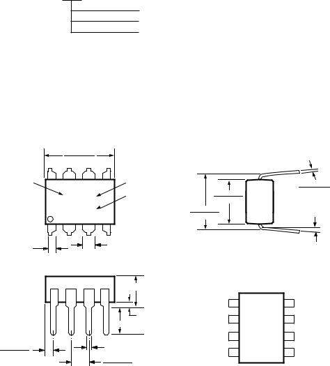
Package Outline Drawings
8-pin DIP Package
|
9.40 (0.370) |
|
|
|
|
|
|
|
9.90 (0.390) |
|
|
|
|
|
|
8 |
7 |
6 |
5 |
REFERENCE VOLTAGE |
|
|
|
TYPE NUMBER |
|
|
|
|
0.18 (0.007) |
||
|
|
|
MATCHING SUFFIX* |
|
|
||
|
|
|
|
|
|
||
|
HP 7860X |
|
DATE CODE |
6.10 (0.240) |
0.33 (0.013) |
||
|
|
|
|||||
|
|
6.60 (0.260) |
|
||||
|
|
|
|
|
|
||
|
|
YYWW |
|
|
7.36 (0.290) |
|
5° TYP. |
|
|
|
|
|
7.88 (0.310) |
|
|
PIN ONE 1 |
2 |
3 |
4 |
|
|
|
|
1.19 (0.047) MAX. |
|
|
1.78 (0.070) MAX. |
|
|
|
|
|
|
|
|
|
|
|
|
|
|
|
|
4.70 (0.185) MAX. |
|
PIN DIAGRAM |
|
PIN ONE
0.76 (0.030)
1.24 (0.049)
0.51 (0.020) MIN. |
2.92 (0.115) MIN. |
0.65 (0.025) MAX. |
2.28 (0.090) |
2.80 (0.110) |
1 VDD1 VDD2 8
2 VIN+ MCLK 7
3 VIN– MDAT 6
4 GND1 GND2 5
DIMENSIONS IN MILLIMETERS AND (INCHES).
*ALL UNITS WITHIN EACH HCPL-7860 STANDARD PACKAGING INCREMENT (EITHER 50 PER TUBE OR 1000 PER REEL) HAVE A COMMON MARKING SUFFIX TO REPRESENT AN ABSOLUTE REFERENCE VOLTAGE TOLERANCE OF ± 1%.
AN ABSOLUTE REFERENCE VOLTAGE TOLERANCE OF ± 4% IS GUARANTEED BETWEEN STANDARD PACKAGING INCREMENTS.
1-267
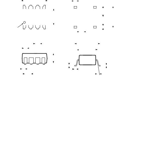
8-pin DIP Gull Wing Surface Mount Option 300
|
|
|
|
|
|
|
|
|
|
|
|
|
|
|
|
|
|
|
|
|
|
|
|
|
|
|
|
|
|
|
|
|
|
|
|
|
PIN LOCATION (FOR REFERENCE ONLY) |
||||||||||||||||||||||||||||||||||||||||||
|
|
|
|
|
|
|
|
|
9.65 ± 0.25 |
|
|
|
|
|
|
|
|
|
|
|
|
|
|
|
|
|
|
|
|
|
1.02 (0.040) |
|
|
|
|
|
|
|
|
|
|
|
|
|
|
|
|||||||||||||||||||||||||||||||||
|
|
|
|
|
|
|
|
|
|
|
|
|
|
|
|
|
|
|
|
|
|
|
|
|
|
|
|
|
|
|
|
|
|
|
|
|
|
|
|||||||||||||||||||||||||||||||||||||||||
|
|
|
|
|
|
|
(0.380 ± 0.010) |
|
|
|
|
|
|
|
|
|
|
|
|
|
|
|
|
|
|
|
|
|
|
|
|
|
|
|
|
|
|
|
|
|
|
|
|
|
|
|
|
|
|||||||||||||||||||||||||||||||
|
|
|
|
|
|
|
|
|
|
|
|
|
|
|
|
|
|
|
|
|
|
|
|
|
|
|
|
|
|
|
|
|
|
|
|
|
1.19 (0.047) |
|
|
|
|
|
|
|
|
|
|
|
|
|
|
|
|||||||||||||||||||||||||||
|
|
|
|
|
|
|
|
|
|
|
|
|
|
|
|
|
|
|
|
|
|
|
|
|
|
|
|
|
|
|
|
|
|
|
|
|
|
|
|
|
|
|
|
|
|
|
|
|
|
|
|
|
|
|
|
|
|
|
|
|
|
|
|
|
|
|
|
|
|
|
|
|
|
|
|
|
|
|
|
|
|
|
|
|
|
|
|
|
|
|
|
|
|
|
|
|
|
|
|
|
|
|
|
|
|
|
|
|
|
|
|
|
|
|
|
|
|
|
|
|
|
|
|
|
|
|
|
|
|
|
|
|
|
|
|
|
|
|
|
|
|
|
|
|
|
|
|
|
|
|
|
|
|
|
|
|
|
|
|
|
|
|
|
|
|
8 |
|
|
|
|
7 |
|
|
|
|
|
6 |
|
|
|
|
|
5 |
|
|
|
|
|
|
|
|
|
|
|
|
|
|
|
|
|
|
|
|
|
|
|
|
|
|
|
|
|
|
|
|
|
|
|
|
|
|
|
|
|
|
|
|
|
|
|
|
|
|
||||||
|
|
|
|
|
|
|
|
|
|
|
|
|
|
|
|
|
|
|
|
|
|
|
|
|
|
|
|
|
|
|
|
|
|
|
|
|
|
|
|
|
|
|
|
|
|
|
|
|
|
|
|
|
|
|
|
|
|
|
|
|
|
|
|
|
|
|
|
||||||||||||
|
|
|
|
|
|
|
|
|
|
|
|
|
|
|
|
|
|
|
|
|
|
|
|
|
|
|
|
|
|
|
|
|
|
|
|
|
|
|
|
|
|
|
|
|
|
|
|
|
|
|
|
|
|
|
|
|
|
|
|
|
|
|
|
|
|
|
|
|
|
4.83 TYP. |
|
|
|||||||
|
|
|
|
|
|
|
|
|
|
|
|
|
|
|
|
|
|
|
|
|
|
|
|
|
|
|
|
|
|
|
|
|
|
|
|
|
|
|
|
|
|
|
|
|
|
|
|
|
|
|
|
|
|
|
|
|
|
|
|
|
|
|
|
|
|
|
|
(0.190) |
|
|
|
|
|||||||
|
|
|
|
|
|
|
|
|
|
|
|
|
|
|
|
|
|
|
|
|
|
|
|
|
|
|
|
|
|
|
|
|
|
|
|
|
|
|
|
|
|
|
|
|
|
|
|
|
|
|
|
|
|
|
|
|
|
|
|
|
|
|
|
|
|
|
|
|
|
|
|
|
|
|
|
|
|
|
|
|
|
|
|
|
|
|
|
|
|
|
|
|
|
|
|
|
|
|
|
|
|
|
|
|
|
|
|
|
|
|
|
|
6.350 ± 0.25 |
|
|
|
|
|
|
|
|
|
|
|
|
|
|
|
|
|
|
|
|
|
|
|
|
|
|
|
|
|
|
|
|
|
|
|
|
|
|
|
|
|
|
|
|||
|
|
|
|
|
|
|
|
|
|
|
|
|
|
|
|
|
|
|
|
|
|
|
|
|
|
|
|
|
|
|
|
|
(0.250 ± 0.010) |
|
|
|
|
|
|
|
|
|
|
|
|
|
|
|
|
|
|
|
|
|
|
|
|
|
|
|
|
|
|
|
9.65 ± 0.25 |
||||||||||||||
|
|
|
|
|
|
|
|
|
|
|
|
|
|
|
|
|
|
|
|
|
|
|
|
|
|
|
|
|
|
|
|
|
|
|
|
|
|
|
|
|
|
|
|
|
|
|
|
|
|
|
|
|
|
|
|
|
|
|
|
|
|
|
|
|
|
|
|
(0.380 ± 0.010) |
|||||||||||
|
|
|
|
|
|
|
|
|
|
|
|
|
|
|
|
|
|
|
|
|
|
|
|
|
|
|
|
|
|
|
|
|
|
|
|
|
|
|
|
|
|
|
|
|
|
|
|
|
|
|
|
|
|
|
|
|
|
|
|
|
|
|
|
|
|
|
|
|
|
|
|
|
|
|
|
|
|
|
|
|
|
|
|
|
|
|
|
|
|
|
|
|
|
|
|
|
|
|
|
|
|
|
|
|
|
|
|
|
|
|
|
|
|
|
|
|
|
|
|
|
|
|
|
|
|
|
|
|
|
|
|
|
|
|
|
|
|
|
|
|
|
|
|
|
|
|
|
|
|
|
|
|
|
|
|
|
|
|
|
MOLDED |
1 |
2 |
|
|
|
3 |
|
|
|
|
4 |
|
|
|
|
|
|
|
|
|
|
|
|
|
|
|
|
|
|
|
|
|
|
|
|
|
|
|
|
|
|
|
|
|
|
|
|
|
|
|
|
|
|
|
|
|
|
|
|
|
|
||||||||||||||||||
|
|
|
|
|
|
|
|
|
|
|
|
|
|
|
|
|
|
|
|
|
|
|
|
|
|
|
|
|
|
|
|
|
|
|
|
|
|
|
|
|
|
|
|
|
|
|
|
|
|
|
|
|
|
|
|
|
|
|
|
|
|
|
|
|
|
|
|
|
|
|
|
|
|
|
|||||
|
|
|
|
|
|
|
|
|
|
|
|
|
|
|
|
|
|
|
|
|
|
|
|
|
|
|
|
|
|
|
|
|
|
|
|
|
|
|
|
|
|
|
|
|
|
|
|
|
|
|
|
|
|
|
|
|
|
|
|
|
|
|
|
|
|
|
|
|
|
|
|
|
|
|
|||||
|
|
|
|
|
|
|
|
|
|
|
|
|
|
|
|
|
|
|
|
|
|
|
|
|
|
|
|
|
|
|
|
|
|
|
|
|
|
|
|
|
|
|
|
|
|
|
|
|
|
|
|
|
|
|
|
|
|
|
|
|
|
|
|
|
|
|
|
|
|
|
|
|
|||||||
|
|
|
|
|
|
|
|
|
|
|
|
|
|
|
|
|
|
|
|
|
|
|
|
|
|
|
|
|
|
|
|
|
|
|
|
|
|
|
|
|
|
|
|
|
|
|
|
|
|
|
|
|
|
|
|
|
|
|
|
|
|
|
|
|
|
|
|
|
|
|
0.380 (0.015) |
||||||||
|
|
|
|
|
|
|
|
|
|
|
|
|
|
|
|
|
|
|
|
|
|
|
|
|
|
|
|
|
|
|
|
|
|
|
|
|
|
|
|
|
|
|
|
|
|
|
|
|
|
|
|
|
|
|
|
|
|
|
|
|
|
|
|
|
|
|
|
||||||||||||
|
|
|
|
|
|
|
|
|
|
|
|
|
|
|
|
|
|
|
|
|
|
|
|
|
|
|
|
|
|
|
|
|
|
|
|
1.19 (0.047) |
|
|
|
|
|
|
|
|
|
|
|
|
0.635 (0.025) |
||||||||||||||||||||||||||||||
|
|
|
|
|
|
|
|
|
|
|
|
|
|
|
|
|
|
|
|
|
|
|
|
|
|
|
|
|
|
|
|
|
|
|
|
1.78 (0.070) |
|
|
|
|
|
|
|
|
|
|
|
|
|
|
|
|
|
|
|
|
|||||||||||||||||||||||
|
|
|
|
|
|
|
|
|
|
|
|
|
|
|
|
|
|
|
|
|
|
|
|
|
|
1.780 |
|
|
|
|
|
|
|
|
|
|
|
|
9.65 ± 0.25 |
|
|
|
|
|
|
|
|
|
|
|
|
|
|
|
|
|
|
||||||||||||||||||||||
|
|
|
|
|
|
|
|
|
|
|
|
|
|
|
|
|
|
|
|
|
|
|
|
|
|
|
|
|
|
|
|
|
|
|
|
|
|
|
|
|
|
|
|
|
|
|
|
|
|
|
|
|
|
|
|
||||||||||||||||||||||||
1.19 |
|
|
|
|
|
|
|
|
|
|
|
|
|
|
|
|
|
|
|
|
|
|
|
|
|
|
(0.070) |
|
|
|
|
|
|
|
|
|
|
|
|
|
|
|
|
|
|
|
(0.380 ± 0.010) |
|
|
|
|
|
|
|
|
|
|
|
|
|
|
|
|
|
|||||||||||||||
|
|
|
|
|
|
|
|
|
|
|
|
|
|
|
|
|
|
|
|
|
|
|
|
|
|
|
|
|
|
|
MAX. |
|
|
|
|
|
|
|
|
|
|
|
|
|
|
|
|
|
7.62 ± 0.25 |
|
|
|
|
|
|
|
|
|
|
|
|
|
|
|
|
|
|
||||||||||||
|
|
|
|
|
|
|
|
|
|
|
|
|
|
|
|
|
|
|
|
|
|
|
|
|
|
|
|
|
|
|
|
|
|
|
|
|
|
|
|
|
|
|
|
|
|
|
|
|
|
|
|
|
|
|
|
|
|
|
|
||||||||||||||||||||
(0.047) |
|
|
|
|
|
|
|
|
|
|
|
|
|
|
|
|
|
|
|
|
|
|
|
|
|
|
|
|
|
|
|
|
|
|
|
|
|
|
|
|
|
|
|
|
|
|
|
|
|
|
|
|
|
|
|
|
|
|
|
|
|
|
|
|
|
|
|
||||||||||||
|
|
|
|
|
|
|
|
|
|
|
|
|
|
|
|
|
|
|
|
|
|
|
|
|
|
|
|
|
|
|
|
|
|
|
|
|
|
|
|
|
|
|
|
|
|
|
|
|
(0.300 ± 0.010) |
|
|
|
|
|
|
|
|
|
|
|
|
|
|
|
|
|
|||||||||||||
MAX. |
|
|
|
|
|
|
|
|
|
|
|
|
|
|
|
|
|
|
|
|
|
|
|
|
|
|
|
|
|
|
|
|
|
|
|
|
|
|
|
|
|
|
|
|
|
|
|
|
|
|
|
|
|
|
|
|
|
|
|
|
|
|
|
||||||||||||||||
|
|
|
|
|
|
|
|
|
|
|
|
|
|
|
|
|
|
|
|
|
|
|
|
|
|
|
|
|
|
|
|
|
|
|
|
|
|
|
|
|
|
|
|
|
|
|
|
|
|
|
|
|
|
|
|
|
|
|
|
|
|
|
|
|
0.255 (0.075) |
||||||||||||||
|
|
|
|
|
|
|
|
|
|
|
|
|
|
|
|
|
|
|
|
|
|
|
|
|
|
|
|
|
|
|
|
|
|
|
|
|
|
|
|
|
|
|
|
|
|
|
|
|
|
|
|
|
|
|
|
|
|
|
|
|
|
|
|
|
|
|
|
|
|
||||||||||
|
|
|
|
|
|
|
|
|
|
|
|
|
|
|
|
|
|
|
|
|
|
|
|
|
|
|
|
|
|
|
|
|
|
|
|
|
|
|
|
|
|
|
|
|
|
|
|
|
|
|
|
|
|
|
|
|
|
|
|
|
|
|
|
|
|
|
|
|
|
||||||||||
|
|
|
|
|
|
|
|
|
|
|
|
|
|
|
|
|
|
|
|
|
|
|
|
|
|
|
|
|
|
|
|
|
|
|
|
|
|
|
|
|
|
|
|
|
|
|
|
|
|
|
|
|
|
|
|
|
|
|
|
|
|
|
|
|
|
|
|
|
|
|
|
|
|
|
|
|
|
|
|
|
|
|
|
|
|
|
|
|
|
|
|
|
|
|
|
|
|
|
|
|
|
|
|
|
|
|
|
|
|
|
|
|
4.19 |
MAX. |
|
|
|
|
|
|
|
|
|
|
|
|
|
|
|
|
|
|
|
|
|
|
|
|
0.010 (0.003) |
||||||||||||||||||||
1.080 ± 0.320 |
|
|
|
|
|
|
|
|
|
|
|
|
|
|
|
|
|
|
|
|
|
|
|
|
|
|
|
(0.165) |
|
|
|
|
|
|
|
|
|
|
|
|
|
|
|
|
|
|
|
|
|
|
|
|
|
|
|
|
|
|
|
|
|
|
|
|
|
|
|
|
|
|
|
|
|||||||
|
|
|
|
|
|
|
|
|
|
|
|
|
|
|
|
|
|
|
|
|
|
|
|
|
|
|
|
|
|
|
|
|
|
|
|
|
|
|
|
|
|
|
|
|
|
|
|
|
|
|
|
|
|
|
|
|
|
|
|
|
|
|
|
|
|
|
|
|
|
|
|
|
|
|
|
|
|
|
|
|
|
|
|
|
|
|
|
|
|
|
|
|
|
|
|
|
|
|
|
|
|
|
|
|
|
|
|
|
|
|
|
|
|
|
|
|
|
|
|
|
|
|
|
|
|
|
|
|
|
|
|
|
|
|
|
|
|
|
|
|
|
|
|
|
|
|
|
|
|
|
|
|
|
|
|
|
|
|
|
|
|
|
|
|
|
|
|
|
|
|
|
|
|
|
|
|
|
|
|
|
|
|
|
|
|
|
|
|
|
|
|
|
|
|
|
|
|
|
|
|
|
|
|
|
|
|
|
|
|
|
|
|
|
|
|
|
|
|
|
|
|
|
|
|
|
|
|
|
|
|
|
|
|
|
|
|
|
|
|
|
|
|
|
|
|
|
|
|
|
|
|
|
|
|
|
|
|
|
|
|
|
|
|
|
|
|
|
|
|
|
|
|
|
|
|
|
|
|
|
|
|
|
|
|
|
|
0.635 ± 0.25 |
|
|
|
|
|
|
|
|
|
|
|
|
|
|
|
|
|
|
||||||||||||||
(0.043 ± 0.013) |
|
|
|
|
|
|
|
|
|
|
|
|
|
|
|
|
|
|
|
|
|
|
|
|
|
|
|
|
|
|
|
|
|
|
|
|
|
|
|
|
|
|
|
|
|
|
|
|
|
|
|
|
|
(0.025 ± 0.010) |
|
|
|
|
|
|
|
|
|
|
|
|
|
|
|
|
|
||||||||
|
|
2.540 |
|
|
|
|
|
|
|
|
|
|
|
|
|
|
|
|
|
|
|
|
|
|
0.51 ± 0.130 |
|
|
|
|
|
|
|
|
|
|
|
|
|
|
|
|
|
|
|
|
12° NOM. |
|||||||||||||||||||||||||||||||||
|
|
|
|
|
|
|
|
|
|
|
|
|
|
|
|
|
|
|
|
|
|
|
|
|
|
|
|
|
|
|
|
|
|
|
|
|
|
|
|
|
|
|
|
|
|
|
|
|
|
|
|
|
|
|
|
|
|
|
|
||||||||||||||||||||
|
|
|
|
|
|
|
|
|
|
|
|
|
|
|
|
|
|
|
|
|
|
|
|
|
|
|
|
|
(0.020 ± 0.005) |
|
|
|
|
|
|
|
|
|
|
|
|
|
|
|
|
|
|
|
|
|
|
|
|
|
|
|
|
|
|
||||||||||||||||||||
|
|
|
|
|
(0.100) |
|
|
|
|
|
|
|
|
|
|
|
|
|
|
|
|
|
|
|
|
|
|
|
|
|
|
|
|
|
|
|
|
|
|
|
|
|
|
|
|
|
|
|
|
|
|
|
|
|
|
|
|
|
|
|
|
|
|
||||||||||||||||
|
|
|
|
|
|
|
|
|
|
|
|
|
|
|
|
|
|
|
|
|
|
|
|
|
|
|
|
|
|
|
|
|
|
|
|
|
|
|
|
|
|
|
|
|
|
|
|
|
|
|
|
|
|
|
|
|
|
|
|
|
|
|
|
|
|
|
|
|
|
||||||||||
|
|
|
|
|
|
|
|
BSC |
|
|
|
|
|
|
|
|
|
|
|
|
|
|
|
|
|
|
|
|
|
|
|
|
|
|
|
|
|
|
|
|
|
|
|
|
|
|
|
|
|
|
|
|
|
|
|
|
|
|
|
|
|
|
|
|
|
|
|
|
|
|
|
||||||||
DIMENSIONS IN MILLIMETERS (INCHES). |
|
|
|
|
|
|
|
|
|
|
|
|
|||||||||||||||||||||||||||||||||||||||||||||||||||||||||||||||||||
TOLERANCES (UNLESS OTHERWISE SPECIFIED): xx.xx = 0.01 |
LEAD COPLANARITY |
||||||||||||||||||||||||||||||||||||||||||||||||||||||||||||||||||||||||||||||
|
|
|
|
|
|
|
|
|
|
|
|
|
|
|
|
|
|
|
|
|
|
|
|
|
|
|
|
|
|
|
|
|
|
|
|
|
|
|
xx.xxx = 0.005 |
MAXIMUM: 0.102 (0.004) |
|||||||||||||||||||||||||||||||||||||||
Package Characteristics
Unless otherwise noted, all specifications are at TA = +25°C.
Parameter |
Symbol |
Min. |
Typ. |
Max. |
Units |
Test Conditions |
Note |
Input-Output Momentary |
VISO |
3750 |
|
|
Vrms |
RH ≤ 50%, t = 1 min. |
14,15 |
Withstand Voltage |
|
|
|
|
|
|
|
(See note ** below) |
|
|
|
|
|
|
|
|
|
|
|
|
|
|
|
Resistance (Input - Output) |
RI-O |
1012 |
1013 |
|
Ω |
VI-O = 500 Vdc |
15 |
|
|
|
|
|
|
|
|
|
|
1011 |
|
|
|
TA = 100°C |
|
|
|
|
|
|
|
||
Capacitance |
CI-O |
|
0.7 |
|
pF |
f = 1 MHz |
|
|
|
|
|||||
(Input - Output) |
|
|
|
|
|
|
|
|
|
|
|
|
|
|
|
Input IC Junction-to-Case |
θjci |
|
96 |
|
°C/W |
Thermocouple located at |
|
Thermal Resistance |
|
|
|
|
|
center underside of |
|
|
|
|
|
|
|
package |
|
Output IC Junction-to-Case |
θjco |
|
114 |
|
°C/W |
|
|
Thermal Resistance |
|
|
|
|
|
|
|
** The Input-Output Momentary Withstand Voltage is a dielectric voltage rating that should not be interpreted as an input-output continuous voltage rating. For the continuous voltage rating refer to your equipment level safety specification or HP Application Note 1074, Optocoupler Input-Output Endurance Voltage.
1-268
Loading...