


HIT HA17324A Datasheet
HA17324/A Series
Quad Operational Amplifier
ADE-204-031 (Z)
1st Edition
Apr. 2000
Description
HA17324 series and HA17324A series are quad operational amplifier that provide high gain and internal
phase compensation, with single power supply. They can be widely used to control equipments.
Features
• Wide range of supply voltage, and single power supply used
• Internal phase compensation
• Wide range of common mode voltage, and possible to operate with an input about 0V
Features only for “A” series
• Low electro-magnetic interference level
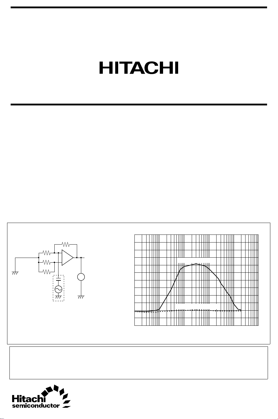
5.0
4.0
3.0
(arb. unit)
2.0
1.0
Output offset voltage
−1.0
100E+3 1E+6 10E+6 100E+6 1E+9 10E+9
Vcc = +7.5 V
Vee = −7.5 V
RF signal source
(for quasi-RF noise)
Rs
Rs
Rf
0.01 µ
Vin
−10 dBm
Rf
−
+
Vout
V
_
(= 100∗Vio)
Notice: The example of an applied circuit or combination with other equipment shown herein indicates
characteristics and performance of semiconductor -applied products.
The company shall assume no responsibility for any problem involving a patent caused when
applying the descriptions in the example.
Output Offset Voltage vs. Input InterferenceMeasurement Condition
HA17324 series
0
HA17324A series
Input RF frequency (Hz)
HA17324/A Series
Ordering Information
HA17324 Series
Type No. Application Package
HA17324P Industrial use DP-14
HA17324FP FP-14DA
HA17324 Commercial use DP-14
HA17324F FP-14DA
HA17324A Series
Type No. Application Package
HA17324AP Industrial use DP-14
HA17324ARP FP-14DN
HA17324AFP FP-14DA
2

Pin Arrangement
HA17324/A Series
Circuit Schematic (1/4)
Vin(−)
Vin(+)
Q1 Q4
Vout1
Vin(−)1
Vin(+)1
V
CC
Vin(+)2
Vin(−)2
Vout2
Q2 Q3
Q8 Q9
1
2
3
4
5
6
7
1
+
−
+
−
2
(Top view)
C
+
+
Q10
14
Vout4
13
Q11
12
11
10
9
8
Q12
Vin(−)4
Vin(+)4
V
EE
Vin(+)3
Vin(−)3
Vout3
Q7
Q5
Q6
Q13
R
1
Vout
4
−
−
3
3
HA17324/A Series
Absolute Maximum Ratings (Ta = 25°C)
Ratings
Item Symbol HA17324/P/AP HA17324F/FP/ARP/AFP Unit
Supply voltage V
CC
Sink current Isink 50 50 mA
Power dissipation P
Common mode input voltage V
T
CM
Differential input voltage Vin (diff) ±V
Operating temperature Topr –20 to +75 –20 to +75 °C
Storage temperature Tstg –55 to +125 –55 to +125 °C
Notes: 1. This is the allowable values up to Ta = 50°C. Derate by 8.3 mW/°C.
2. Tjmax = θj-a · P
max + Ta (θj-a; Thermal resistor between junction and ambient at set board
C
use).
The wiring density and the material of the set board must be chosen for thermal conductance of
efficacy board.
And P
max cannot be over the value of PT.
C
32 32 V
1
625 *
–0.3 to V
CC
CC
2
625 *
–0.3 to V
±V
CC
CC
mW
V
V
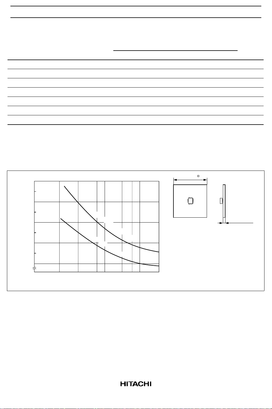
(°C)
Thermal resistor θj-a
240
220
200
180
160
140
120
100
80
ab
SOP14 − with compound
SOP14
−
no compound
0.5 1 2 5 10 20
Thermal conductance of efficacy board (W/m °C)
40 mm
1.5 t epoxy
a. Class epoxy board of 10% wiring density
b. Class epoxy board of 30% wiring density
4
 Loading...