

HIT HM62256AFP-10T, HM62256AFP-12T, HM62256AFP-15T, HM62256AFP-8T, HM62256ALFP-10SLT Datasheet
...
HM62256A Series
32,768-word × 8-bit High Speed CMOS Static RAM
Maintenance only
The Hitachi HM62256A is a CMOS static RAM
organized 32-kword × 8-bit. It realizes higher
performance and low power consumption by
employing 0.8 µm Hi-CMOS process technology.
The device, packaged in a 8 × 14 mm TSOP with
thickness of 1.2 mm, 450-mil SOP (foot print pitch
width), 600-mil plastic DIP, or 300-mil plastic DIP,
is available for high density mounting. TSOP
package is suitable for cards, and reverse type
TSOP is also provided. It offers low power
standby power dissipation; therefore, it is suitable
for battery back up system.
Features
• High speed: Fast Access time 85/100/120/150 ns
(max)
• Low Power
Standby: 5 µW (typ) (L/L-SL version)
Operation: 40 mW (typ) (f = 1 MHz)
• Single 5 V supply
• Completely static memory
No clock or timing strobe required
• Equal access and cycle times
• Common data input and output: Three state
output
• Directly TTL compatible: All inputs and outputs
• Capability of battery back up operation
Ordering Information
Type No. Access time Package
——————————————————————–
HM62256AP-8 85 ns 600-mil
HM62256AP-10 100 ns 28-pin
HM62256AP-12 120 ns plastic DIP
HM62256AP-15 150 ns (DP-28)
————————————————–
HM62256ALP-8 85 ns
HM62256ALP-10 100 ns
HM62256ALP-12 120 ns
HM62256ALP-15 150 ns
————————————————–
HM62256ALP-8SL 85 ns
HM62256ALP-10SL 100 ns
HM62256ALP-12SL 120 ns
HM62256ALP-15SL 150 ns
——————————————————————–
HM62256ASP-8 85 ns 300-mil
HM62256ASP-10 100 ns 28-pin
HM62256ASP-12 120 ns plastic DIP
HM62256ASP-15 150 ns (DP-28NA)
————————————————–
HM62256ALSP-8 85 ns
HM62256ALSP-10 100 ns
HM62256ALSP-12 120 ns
HM62256ALSP-15 150 ns
————————————————–
HM62256ALSP-8SL 85 ns
HM62256ALSP-10SL 100 ns
HM62256ALSP-12SL 120 ns
HM62256ALSP-15SL 150 ns
——————————————————————–
HM62256AFP-8T 85 ns 450-mil
HM62256AFP-10T 100 ns 28-pin
HM62256AFP-12T 120 ns plastic SOP
HM62256AFP-15T 150 ns (FP-28DA)
————————————————–
HM62256ALFP-8T 85 ns
HM62256ALFP-10T 100 ns
HM62256ALFP-12T 120 ns
HM62256ALFP-15T 150 ns
————————————————–
HM62256ALFP-8SLT 85 ns
HM62256ALFP-10SLT 100 ns
HM62256ALFP-12SLT 120 ns
HM62256ALFP-15SLT 150 ns
——————————————————————–
Note: This device is not available for new application.
1
HM62256A Series HM62256A Series
TSOP Series
Type No. Access time Package
——————————————————————–
HM62256ALT-8 85 ns 8 mm × 14 mm
HM62256ALT-10 100 ns 32-pin TSOP
HM62256ALT-12 120 ns (normal type)
HM62256ALT-15 150 ns (TFP-32DA)
———————————————–
HM62256ALT-8SL 85 ns
HM62256ALT-10SL 100 ns
HM62256ALT-12SL 120 ns
HM62256ALT-15SL 150 ns
——————————————————————–
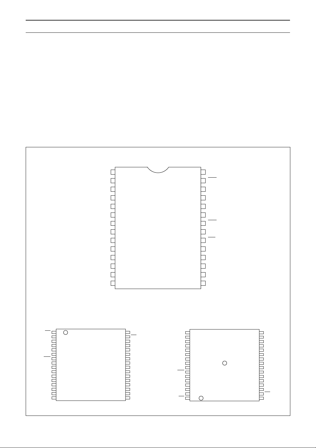
Pin Arrangement
HM62256AP/AFP/ASP Series
A7
A6
A5
A4
A3
A2
A1
A0
V
SS
1
2
3
4
5
6
7
8
9
10
11
12
13
14
A14
A12
I/O0
I/O1
I/O2
Type No. Access time Package
——————————————————————–
HM62256ALR-8 85 ns 8 mm × 14 mm
HM62256ALR-10 100 ns 32-pin TSOP
HM62256ALR-12 120 ns (reverse type)
HM62256ALR-15 150 ns (TFP-32DAR)
———————————————–
HM62256ALR-8SL 85 ns
HM62256ALR-10SL 100 ns
HM62256ALR-12SL 120 ns
HM62256ALR-15SL 150 ns
——————————————————————–
V
28
CC
WE
27
A13
26
A8
25
A9
24
A11
23
OE
22
A10
21
CS
20
I/O7
19
I/O6
18
I/O5
17
I/O4
16
I/O3
15
HM62256AT Series
OE
1
A11
2
NC
3
A9
4
A8
5
A13
6
WE
7
V
8
CC
A14
9
A12
10
A7
11
A6
12
A5
13
NC
14
A4
15
A3
16
2
(Top view)
(Top view)
HM62256AR Series
32
A10
31
CS
30
NC
29
I/O7
28
I/O6
27
I/O5
26
I/O4
25
I/O3
24
V
SS
23
I/O2
22
I/O1
21
I/O0
20
A0
19
NC
18
A1
17
A2
NC
A12
A14
V
WE
A13
NC
A11
OE
A3
16
A4
15
14
A5
13
A6
12
A7
11
10
9
8
CC
7
6
A8
5
A9
4
3
2
1
(Top view)
A2
17
A1
18
NC
19
A0
20
I/O0
21
I/O1
22
I/O2
23
V
24
SS
I/O3
25
I/O4
26
I/O5
27
I/O6
28
I/O7
29
NC
30
CS
31
A10
32

HM62256A Series HM62256A Series
Pin Description
Symbol Function
——————————————————————–
A0 – A14 Address
——————————————————————–
I/O0 – I/O7 Input/output
——————————————————————–
CS Chip select
——————————————————————–
WE Write enable
——————————————————————–
Block Diagram
A5
A4
A3
A11
A9
A8
A12
•
•
•
•
•
•
•
Row
Decoder
•
•
•
Symbol Function
——————————————————————–
OE Output enable
——————————————————————–
NC No connection
——————————————————————–
V
CC
Power supply
——————————————————————–
V
SS
Ground
——————————————————————–
V
CC
V
SS
Memory Matrix
×
512 512
A7
A6
I/O0
I/O7
CS
WE
OE
•
•
•
•
•
•
•
•
•
•
•
Input
Data
Control
•
Column I/O
Column Decoder
A1 A2 A10 A14A13
A0
•
•
•
•
•
•
•
•
•
Timing Pulse Generator
Read/Write Control
3

HM62256A Series HM62256A Series
Function Table
WE CS OE Mode VCCcurrent I/O pin Ref. cycle
———————————————————————————————————————————————–
X H X Not selected I
———————————————————————————————————————————————–
H L H Output disable I
———————————————————————————————————————————————–
H L L Read I
———————————————————————————————————————————————–
L L H Write I
———————————————————————————————————————————————–
LLLWrite I
———————————————————————————————————————————————–
Note: X: H or L
Absolute Maximum Ratings
Parameter Symbol Value Unit
———————————————————————————————————————————————–
Voltage on any pin relative to V
SS
———————————————————————————————————————————————–
Power dissipation P
———————————————————————————————————————————————–
Operating temperature Topr 0 to +70 °C
———————————————————————————————————————————————–
Storage temperature Tstg –55 to +125 °C
———————————————————————————————————————————————–
Storage temperature under bias Tbias –10 to +85 °C
———————————————————————————————————————————————–
Note: 1. V
min = –3.0 V for pulse half-width ≤ 50 ns
T
V
T
T
SB
CC
CC
CC
CC
, I
SB1
–0.5*1to +7.0 V
1.0 W
High-Z —
High-Z —
Dout Read cycle (1)–(3)
Din Write cycle (1)
Din Write cycle (2)
Recommended DC Operating Conditions (Ta = 0 to +70°C)
Parameter Symbol Min Typ Max Unit
———————————————————————————————————————————————–
Supply voltage V
CC
———————————————————————————————–
V
SS
———————————————————————————————————————————————–
Input high (logic 1) voltage V
IH
———————————————————————————————————————————————–
Input low (logic 0) voltage V
IL
———————————————————————————————————————————————–
Note: 1. V
min = –3.0 V for pulse half-width ≤ 50 ns
IL
4
4.5 5.0 5.5 V
000V
2.2 — 6.0 V
*1
–0.5
— 0.8 V

HM62256A Series HM62256A Series
DC Characteristics (Ta = 0 to +70°C, VCC= 5 V ± 10%, VSS= 0 V)
Parameter Symbol Min Typ*1Max Unit Test conditions
———————————————————————————————————————————————–
Input leakage current |I
———————————————————————————————————————————————–
Output leakage current |I
———————————————————————————————————————————————–
Operating V
current I
CC
——————————————————————————————————————————
HM62256A-8 I
HM62256A-10 — 30 50 CS = V
HM62256A-12 — 27 45
HM62256A-15 — 24 40
——————————————————————————————————————————
———————————————————————————————————————————————–
Standby V
current I
CC
———————————————————————————————————————————————–
Output low voltage V
———————————————————————————————————————————————–
Output high voltage V
———————————————————————————————————————————————–
Notes: 1. Typical values are at V
2. This characteristics is guaranteed only for L-version.
3. This characteristics is guaranteed only for L-SL version.
| — — 1 µA Vin = VSSto V
LI
|——1 µACS = VIHor OE = VIHor WE = VIL,
LO
CC
— 6 15 mA CS = VIL, others = VIH/V
V
I/O
= VSSto V
CC
CC
IL
Iout = 0 mA
CC1
I
CC2
SB
— 33 50 mA min cycle, duty = 100%, I
, others = VIH/V
IL
— 5 15 mA Cycle time = 1µs, I
CS = V
— 0.3 2 mA CS = V
, VIH= VCC, VIL= 0
IL
IH
I/O
I/O
IL
= 0 mA
= 0 mA
———————————————————————————————————
I
SB1
— 0.01 1 mA Vin ≥ 0 V
—————————————— CS ≥ V
— 0.3
*2
100*2µA
CC
– 0.2 V
——————————————
OL
OH
— 0.3
*3
— — 0.4 V IOL= 2.1 mA
2.4 — — V IOH= –1.0 mA
= 5.0 V, Ta = +25°C and not guaranteed.
CC
50
*3
µA
Capacitance (Ta = 25°C, f = 1 MHz)
*1
Parameter Symbol Min Typ Max Unit Test conditions
———————————————————————————————————————————————–
Input capacitance Cin — — 6 pF Vin = 0 V
———————————————————————————————————————————————–
Input/output capacitance C
I/O
——8 pFV
I/O
= 0 V
———————————————————————————————————————————————–
Note: 1. This parameter is sampled and not 100% tested.
5

HM62256A Series HM62256A Series
AC Characteristics (Ta = 0 to +70°C, VCC= 5 V ± 10%, unless otherwise noted.)
Test Conditions
• Input pulse levels: 0.8 V to 2.4 V
• Input and output timing refernce levels: 1.5 V
• Input rise and fall times: 5 ns
• Output load: 1 TTL Gate + CL(100 pF)
(Including scope & jig)
Read Cycle
HM62256A-8 HM62256A-10 HM62256A-12 HM62256A-15
—————– —————– —————– —————–
Parameter Symbol Min Max Min Max Min Max Min Max Unit Note
———————————————————————————————————————————————–
Read cycle time t
———————————————————————————————————————————————–
Address access time t
———————————————————————————————————————————————–
Chip select t
access time
———————————————————————————————————————————————–
Output enable to t
output valid
———————————————————————————————————————————————–
Chip selection to t
output in low-Z
———————————————————————————————————————————————–
Output enable to t
output in low-Z
———————————————————————————————————————————————–
Chip deselection to t
output in high-Z
———————————————————————————————————————————————–
Output disable to t
output in high-Z
———————————————————————————————————————————————–
Output hold from t
address change
———————————————————————————————————————————————–
RC
AA
ACS
OE
CLZ
OLZ
CHZ
OHZ
OH
85 — 100 — 120 — 150 — ns
— 85 — 100 — 120 — 150 ns
— 85 — 100 — 120 — 150 ns
— 45 — 50 — 60 — 70 ns
10 — 10 — 10 — 10 — ns 2
5—5—5—5—ns2
0 30 0 35 0 40 0 50 ns 1, 2
0 30 0 35 0 40 0 50 ns 1, 2
5 — 10 — 10 — 10 — ns
6

HM62256A Series HM62256A Series
Read Timing Waveform (1)
Address
CS
OE
Dout
Read Timing Waveform (2)
*3
*3 *4 *6
t
t
CLZ
AA
t
t
OE
t
ACS
*2
OLZ
t
RC
t
OH
*2
*1 *2
t
OHZ
*1 *2
t
CHZ
Valid Data
Address
Dout
t
RC
t
t
t
OH
AA
OH
Valid Data
7

HM62256A Series HM62256A Series
Read Timing Waveform (3)
*3 *5 *6
CS
t
Dout
Notes: 1. t
CHZ
and t
ACS
*2
t
CLZ
Valid Data
are defined as the time at which the outputs achieve the open circuit
OHZ
t
CHZ
*1,*2
conditions and are not referenced to output voltage levels.
2. This parameter is sampled and not 100% tested.
3. WE is high for read cycle.
4. Device is continuously selected, CS = V
.
IL
5. Address Valid prior to or coincident with CS transition Low.
6. OE = V
.
IL
Write Cycle
HM62256A-8 HM62256A-10 HM62256A-12 HM62256A-15
—————– —————– —————– —————–
Parameter Symbol Min Max Min Max Min Max Min Max Unit Note
———————————————————————————————————————————————–
Write cycle time t
WC
———————————————————————————————————————————————–
Chip selection to t
CW
end of write
———————————————————————————————————————————————–
Address setup time t
AS
———————————————————————————————————————————————–
Address valid to t
AW
end of write
———————————————————————————————————————————————–
Write pulse width t
WP
———————————————————————————————————————————————–
Write recovery time t
WR
———————————————————————————————————————————————–
WE to output in high-Z t
WHZ
———————————————————————————————————————————————–
Data to write time t
DW
overlap
———————————————————————————————————————————————–
Data hold from t
DH
write time
———————————————————————————————————————————————–
Output active from t
OW
end of write
———————————————————————————————————————————————–
Output disable to t
OHZ
output in high-Z
———————————————————————————————————————————————–
85 — 100 — 120 — 150 — ns
75 — 80 — 85 — 100 — ns 2
0—0—0—0—ns3
75 — 80 — 85 — 100 — ns
55 — 60 — 70 — 90 — ns 1
0—0—0—0—ns4
0 30 0 35 0 40 0 50 ns 10
40 — 40 — 50 — 60 — ns
0—0—0—0—ns
5—5—5—5—ns10
0 30 0 35 0 40 0 50 ns 10, 11
8

HM62256A Series HM62256A Series
Write Timing Waveform (1) (OEClock)
t
WC
Address
OE
CS
WE
Dout
Din
t
AW
*2
t
CW
*6
*3
t
AS
*5 *10
t
OHZ
t
WP
t
*1
DW
t
WR
t
*4
DH
Valid Data
9

HM62256A Series HM62256A Series
Write Timing Waveform (2) (OELow Fixed)
t
WC
Address
*2
t
CW
*4
t
WR
CS
*6
t
AW
*1
t
WP
t
WE
*3
t
AS
t
WHZ
*5 *10
t
OW
OH
*10
*7
Dout
Din
t
DW
Valid Data
t
DH
*9
Notes: 1. A write occurs during the overlap of a low CS and a low WE. A write begins at the later
transition of CS going low or WE going low. A write ends at the earlier transition of CS
going high or WE going high. t
is measured from the beginning of write to the end of
WP
write.
2. t
3. t
4. t
is measured from CS going low to the end of write.
CW
is measured from the address valid to the beginning of write.
AS
is measured from the earlier of WE or CS going high to the end of write cycle.
WR
5. During this period, I/O pins are in the output state so that the input signals of the opposite
phase to the outputs must not be applied.
6. If the CS low transition occurs simultaneously with the WE low transition or after the WE
transition, the output remain in a high impedance state.
7. Dout is the same phase of the write data of this write cycle.
8. Dout is the read data of next address.
9. If CS is low during this period, I/O pins are in the output state. Therefore, the input signals
of the opposite phase to the output must not be applied to them.
10. This parameter is sampled and not 100% tested.
11. t
OHZ
and t
are defined as the time at which the outputs achieve the open circuit
WHZ
conditions and are not referenced to output voltage levels.
*8
10

HM62256A Series HM62256A Series
Low VCCData Retention Characteristics (Ta = 0 to +70°C)
This characteristics is guaranteed only for L/L-SL version.
Parameter Symbol Min Typ*1Max Unit Test conditions
———————————————————————————————————————————————–
V
for data retention V
CC
DR
———————————————————————————————————————————————–
Data retention current I
CCDR
———————————————————————————————————————————————–
Chip deselect to data retention time t
CDR
——————————————————————————————————––
Operation recovery time t
R
———————————————————————————————————————————————–
Low VCCData Retention Timing Waveform
V
CC
4.5 V
2 ——VCS ≥VCC– 0.2 V, Vin ≥ 0 V
— 0.2 30
*2
µA VCC= 3.0 V, Vin ≥ 0 V
——————————————–
— 0.2 10
*3
µA CS ≥ VCC– 0.2 V
0 — — ns See retention waveform
*4
t
RC
——ns
Data retention mode
t
CDR
2.2 V
V
DR
CS
0 V
≥
CS V – 0.2 V
CC
Notes: 1 Typical values are at VCC= 3.0 V, Ta = +25°C and not guaranteed.
2. 20 µA max at Ta = 0 to +40°C. (only for L-version)
3. 3 µA max at Ta = 0 to +40°C. (only for L-SL version)
4. t
= read cycle time.
RC
5. CS controls address buffer, WE buffer, OE buffer, and Din buffer. If CS controls data
retention mode, Vin levels (address, WE, OE, I/O) can be in the high impedance state.
t
R
11
 Loading...