


HA13155
33 W × 4-Channel BTL Power IC
ADE-207-187A (Z) 2nd Edition Jul. 1999
Description
The HA13155 is four-channel BTL amplifier IC designed for car audio, featuring high output and low distortion, and applicable to digital audio equipment. It provides 33 W output per channel, with a 13.7 V power supply and at Max distortion.
Functions
•4 ch BTL power amplifiers
•Built-in standby circuit
•Built-in muting circuit
•Built-in protection circuit (surge, T.S.D, and ASO)
Features
•Requires few external parts
•Popping noise minimized
•Low output noise
•Built-in high reliability protection circuit
•Pin to pin with HA13150A/HA13151/HA13152/HA13153

HA13155
Block Diagram
|
|
|
|
|
C11 |
|
|
|
|
|
|
|
0.1 μ/16 V |
|
VCC |
|
|
|
|
|
C9 |
|
|
|
|
|
|
|
|
13.2 V |
|
|
|
|
|
|
4400 μ/16 V |
|
|
|
|
14 |
|
6 |
|
|
|
|
|
18 |
|
|
|
||
2 |
STBY |
IN VCC |
PVCC2 |
PVCC1 |
3 |
|
|
|
|
|
|
|
|||
|
|
|
|
|
R1 |
|
|
|
IN-1 |
|
|
|
2.2 |
C1 |
|
1 |
|
Buffer & Mute-1 |
Amp-1 |
4 |
|
||
|
|
|
|
|
|
0.1 μ |
|
|
|
|
|
|
5 |
|
|
|
|
|
|
|
R2 |
C2 |
|
|
|
|
|
|
2.2 |
0.1 μ |
|
|
|
|
|
|
7 |
|
|
|
IN-2 |
|
|
|
R3 |
|
|
11 |
|
|
|
|
2.2 |
C3 |
|
|
Buffer & Mute-2 |
Amp-2 |
8 |
|
|||
|
|
|
|
|
|
0.1 μ |
|
|
|
|
|
|
9 |
|
|
|
|
|
|
|
R4 |
C4 |
|
|
|
|
|
|
2.2 |
0.1 μ |
|
|
|
|
|
|
15 |
|
|
|
IN-3 |
|
|
|
R5 |
|
|
|
|
|
|
2.2 |
|
|
|
|
|
|
|
Amp-3 |
C5 |
|
|
13 |
|
Buffer & Mute-3 |
16 |
|
|||
|
|
|
|
|
|
0.1 μ |
|
|
|
|
|
|
17 |
|
|
|
|
|
|
|
R6 |
C6 |
|
|
|
|
|
|
2.2 |
0.1 μ |
|
|
|
|
|
|
19 |
|
|
|
IN-4 |
|
|
|
R7 |
|
|
|
|
|
|
2.2 |
|
|
|
23 |
|
Buffer & Mute-4 |
Amp-4 |
C7 |
|
||
|
20 |
|
|||||
|
|
|
|
|
|
0.1 μ |
|
|
MUTE |
Protector |
|
|
21 |
|
|
10 |
|
(ASO, Surge, TSD) |
|
R8 |
C8 |
|
|
R9 |
|
|
|
|
|
||
|
|
|
|
2.2 |
0.1 μ |
|
|
7.5 k |
|
12 |
|
22 |
|
||
|
C10 |
TAB |
|
|
|||
|
|
|
|
|
|
R: Ω |
|
|
|
|
10 μ/10 V |
|
|
Unit |
|
|
|
|
|
|
|
|
C: F |
C1 to C8 should be polyester film capacitors with no secondary resonance (non-inductive), to assure stable operation.
Notes: |
1. |
Standby |
5 V |
|
2 |
|
|||
|
|
Power is turned on when a signal of |
37.5 k |
Q1 ON |
|
|
3.5 V or 0.05 mA is impressed at pin 2. |
23.5 k |
↓ |
|
|
When pin 2 is open or connected to |
BIAS ON |
|
|
|
|
|
|
|
|
GND, standby is turned on (output off). |
|
|
2. Muting |
5 V |
|
|
|
|
|
|
|
|
|
|
|
|
|
|
Muting is turned off (output on) when |
|
|
|
10 |
|
|
|
|
|
|
|
|
|||
a signal of 3.5 V or 0.2 mA is impressed |
|
|
|
|
|
|
|
|
|
|
|
|
|
Q2 ON |
|
|
|
|
|
|
|
|
|
|
|
|
|
|
|
||
at pin 10. |
|
|
|
|
|
|
25 k |
|
|
|
|
|
|
↓ |
|
|
|
|
|
|
|
|
|
|
|
|
|
|
|||
When pin 10 is open or connected to |
|
|
|
|
|
|
|
|
|
|
MUTE ON |
|
|||
|
|
|
|
|
|
|
|
|
|
|
|
|
|
|
|
GND, muting is turned on (output off). |
|
|
|
|
|
|
|
|
|
|
|
|
|
|
|
|
|
|
|
|
|
|
|
|
|
|
|
|
|
|
|
|
|
|
|
|
|
|
|
|
|
|
|
|
|
|
|
|
|
|
|
|
|
|
|
|
|
|
|
|
|
|
|
3. TAB (header of IC) connected to GND.
2
HA13155
Absolute Maximum Ratings
Item |
Symbol |
Rating |
Unit |
Operating supply voltage |
VCC |
18 |
V |
Supply voltage when no signal*1 |
VCC (DC) |
26 |
V |
|
|
|
|
Peak supply voltage*2 |
VCC (PEAK) |
50 |
V |
|
|
|
|
Output current*3 |
IO (PEAK) |
4 |
A |
|
|
|
|
Power dissipation*4 |
PT |
83 |
W |
|
|
|
|
Junction temperature |
Tj |
150 |
°C |
Operating temperature |
Topr |
–30 to +85 |
°C |
Storage temperature |
Tstg |
–55 to +125 |
°C |
Notes: 1. Tolerance within 30 seconds.
2.Tolerance in surge pulse waveform.
3.Value per 1 channel.
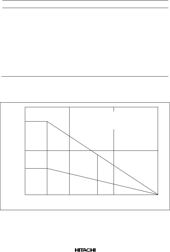
4.Value when attached on the infinite heat sink plate at Ta = 25 °C. The derating carve is as shown in the graph below.
|
100 |
|
|
|
|
|
|
|
83 W |
|
A: When heat sink is infinite (θj-a = 1.5°C/W) |
|
|
|
|
|
B: When θf (thermal resistance of heat sink) = 3°C/W |
|||
|
|
|
|
(θj-a = 4.5°C/W) |
|
|
(W) |
|
|
|
|
|
|
T |
|
|
|
A |
|
|
P |
|
|
|
|
|
|
|
|
|
|
|
|
|
dissipation |
50 |
|
|
|
|
|
|
|
|
|
|
|
|
Power |
|
28 W |
|
|
|
|
|
|
|
|
|
|
|
|
|
|
|
B |
|
|
|
0 |
25 |
50 |
85 |
100 |
150 |
|
|
|
Ambient temperature Ta |
(°C) |
|
|
3

HA13155
Electrical Characteristics (VCC = 13.2 V, f = 1 kHz, RL = 4 Ω, Rg = 600 Ω, Ta = 25°C)
Item |
Symbol |
Min |
|
|
|
Typ |
|
Max |
Unit |
|
Test Conditions |
||||||||||||
Quiescent current |
IQ1 |
— |
300 |
|
|
|
|
|
— |
mA |
Vin = 0 |
|
|||||||||||
|
|
|
|
|
|
|
|
|
|
|
|
|
|
||||||||||
Output offset voltage |
VQ |
–250 |
0 |
|
|
|
|
|
+250 |
mV |
|
|
|
||||||||||
|
|
|
|
|
|
|
|
|
|
|
|
|
|
|
|
|
|||||||
Gain |
GV |
30.5 |
|
|
|
|
32 |
|
|
|
|
33.5 |
dB |
|
|
|
|||||||
|
|
|
|
|
|
|
|
|
|
|
|
|
|
||||||||||
Gain difference between |
GV |
–1.0 |
0 |
|
|
|
|
|
+1.0 |
dB |
|
|
|
||||||||||
channels |
|
|
|
|
|
|
|
|
|
|
|
|
|
|
|
|
|
|
|
|
|
|
|
|
|
|
|
|
|
|
|
|
|
|
|
|
|
||||||||||
Rated output power |
Po |
— |
19 |
|
|
|
|
|
|
— |
W |
V |
CC = 13.2 V |
||||||||||
|
|
|
|
|
|
|
|
|
|
|
|
|
|
|
|
|
|
|
|
|
|
THD = 10%, RL = 4 Ω |
|
|
|
|
|
|
|
|
|
|
|
|
|
|
|
||||||||||
Max output power |
Pomax |
— |
33 |
|
|
|
|
|
|
— |
W |
V |
CC = 13.7 V, RL = 4 Ω |
||||||||||
|
|
|
|
|
|
|
|
|
|
|
|
|
|||||||||||
Total harmonic distortion |
T.H.D. |
— |
0.02 |
|
|
|
|
|
— |
% |
Po = 3 W |
|
|||||||||||
|
|
|
|
|
|
|
|
|
|
|
|
|
|||||||||||
Output noise voltage |
WBN |
— |
0.15 |
|
|
|
|
|
— |
mVrms |
Rg = 0 |
Ω |
|||||||||||
|
|
|
|
|
|
|
|
|
|
|
|
|
|
|
|
|
|
|
|
|
|
BW = 20 to 20 kHz |
|
|
|
|
|
|
|
|
|
|
|
|
|
|
|||||||||||
Ripple rejection |
SVR |
— |
55 |
|
|
|
|
|
|
— |
dB |
Rg = 600 Ω, f = 120 Hz |
|||||||||||
|
|
|
|
|
|
|
|
|
|
|
|
|
|
||||||||||
Channel cross talk |
C.T. |
— |
70 |
|
|
|
|
|
|
— |
dB |
Rg = 600 |
Ω |
||||||||||
|
|
|
|
|
|
|
|
|
|
|
|
|
|
|
|
|
|
|
|
|
|
Vout = 0 dBm |
|
|
|
|
|
|
|
|
|
|
|
|
|
|
|
|
|||||||||
Input impedance |
Rin |
— |
25 |
|
|
|
|
|
|
— |
k Ω |
|
|
|
|||||||||
|
|
|
|
|
|
|
|
|
|
||||||||||||||
Standby current |
IQ2 |
— |
|
— |
10 |
µA |
|
|
|
||||||||||||||
|
|
|
|
|
|
|
|
|
|
|
|
|
|
|
|
|
|||||||
Standby control voltage |
VSTH |
3.5 |
|
|
|
|
|
|
|
— |
|
V CC |
V |
|
|
|
|||||||
(high) |
|
|
|
|
|
|
|
|
|
|
|
|
|
|
|
|
|
|
|
|
|
|
|
|
|
|
|
|
|
|
|
|
|
|
|
|
|
|
|
||||||||
Standby control voltage |
VSTL |
0 |
|
|
|
|
|
|
|
— |
1.5 |
V |
|
|
|
||||||||
(low) |
|
|
|
|
|
|
|
|
|
|
|
|
|
|
|
|
|
|
|
|
|
|
|
|
|
|
|
|
|
|
|
|
|
|
|
|
|
|
|
|
|||||||
Muting control voltage |
VMH |
3.5 |
|
|
|
|
|
|
|
— |
|
V CC |
V |
|
|
|
|||||||
(high) |
|
|
|
|
|
|
|
|
|
|
|
|
|
|
|
|
|
|
|
|
|
|
|
|
|
|
|
|
|
|
|
|
|
|
|
|
|
|
|
||||||||
Muting control voltage |
VML |
0 |
|
|
|
|
|
|
|
— |
1.5 |
V |
|
|
|
||||||||
(low) |
|
|
|
|
|
|
|
|
|
|
|
|
|
|
|
|
|
|
|
|
|
|
|
|
|
|
|
|
|
|
|
|
|
|
|
|
|||||||||||
Muting attenuation |
ATTM |
— |
70 |
|
|
|
|
|
|
— |
dB |
Vout = 0 dBm |
|||||||||||
|
|
|
|
|
|
|
|
|
|
|
|
|
|
|
|
|
|
|
|
|
|
|
|
|
|
|
|
|
|
|
|
|
|
|
|
|
|
|
|
|
|
|
|
|
|
|
|
4
 Loading...