


HIT 4AK19 Datasheet
Features
• Low on-resistance
N Channel: R
≤ 0.5 Ω, VGS = 10 V, ID = 2.5 A
DS(on)
R
≤ 0.6 Ω, VGS = 4 V, ID = 2.5 A
DS(on)
• 4 V gate drive devices.
• High density mounting
Outline
4AK19
Silicon N Channel MOS FET
High Speed Power Switching
ADE-208-727 (Z)
1st. Edition
February 1999
SP-10
G
2
1
1
2
3
10
4
5
6
7
8
9
10
1, 10. Source
2, 4, 6, 8. Gate
3, 5, 7, 9. Drain
3
D
4
G
S
5
D
6
G
7
D
8
G
9
D
S

4AK19
Absolute Maximum Ratings (Ta = 25°C)
Item Symbol Ratings Unit
Drain to source voltage V
Gate to source voltage V
Drain current I
Drain peak current I
Body-drain diode reverse drain current I
DSS
GSS
D
D(pulse)
DR
Note1
Channel dissipation Pch(Tc = 25°C)
Channel dissipation Pch
Note2
Channel temperature Tch 150 °C
Storage temperature Tstg –55 to +150 °C
Note: 1. PW ≤ 10 µs, duty cycle ≤ 1%
2. 4 devices poeration
Electrical Characteristics (Ta = 25°C)
Item Symbol Min Typ Max Unit Test Conditions
Drain to source breakdown voltage V
Gate to source breakdown voltage V
Zero gate voltege drain current I
Gate to source leak current I
Gate to source cutoff voltage V
Static drain to source on state
(BR)DSS
(BR)GSS
DSS
GSS
GS(off)
R
DS(on)
resistance
Static drain to source on state
R
DS(on)
resistance
Forward transfer admittance |yfs|35—SI
Input capacitance Ciss — 25 — pF VDS = 10 V
Output capacitance Coss — 140 — pF VGS = 0
Reverse transfer capacitance Crss — 3 — pF f = 1 MHz
Gate series resistance Rg — 2.5 — kΩ VDS = 0, VGS = 0, f = 1 MHz
Turn-on delay time t
Rise time t
Turn-off delay time t
Fall time t
Body–drain diode forward voltage V
Body–drain diode reverse
t
d(on)
r
d(off)
f
DF
rr
recovery time
Note: 3. Pulse test
120 — — V ID = 10 mA, VGS = 0
±20——V I
— — 100 µAVDS = 100 V, VGS = 0
——±10 µAVGS = ±16 V, VDS = 0
1.0 — 2.0 V ID = 1 mA, VDS = 10 V
— 0.3 0.5 Ω ID = 2.5 A, VGS = 10 V
— 0.35 0.6 Ω ID = 2.5 A, VGS = 4 V
— 0.3 — µsVGS = 10 V, ID = 2.5 A
— 0.45 — µsR
— 6.6 — µs
— 1.4 — µs
— 1.1 — V IF = 5 A, VGS = 0
— 600 — ns IF = 5 A, VGS = 0
120 V
±20 V
5A
10 A
5A
Note2
28 W
3.5 W
= ±100 µA, VDS = 0
G
= 2.5 A, VDS = 10 V
D
= 12 Ω
L
diF/ dt = 50A/ µs
Note3
Note3
Note3
2
Main Characteristics
4AK19
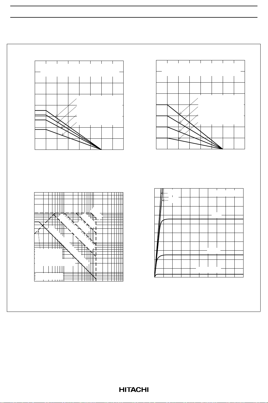
Maximum Channel Dissipation Curve
8
Condition : Channel dissipation of
each die is idetical
6
4 Device Operation
4
3 Device Operation
2 Device Operation
1 Device Operation
2
Channel Dissipation Pch (W)
0
50 100 150 200
Ambient Temperature Ta (°C)
Maximum Safe Operation Area
50
20
10
D
5
PW = 10 ms (1shot)
DC Operation (Tc = 25°C)
10 µs
100 µs
1 ms
2
1
0.5
Operation in
Drain Current I (A)
this area is
0.2
limited by R
DS(on)
0.1
Ta = 25 °C
0.05
1 3 10 30 100 300 1000
Drain to Source Voltage V (V)
DS
Maximum Channel Dissipation Curve
46
Condition : Channel dissipation of
each die is idetical
32
4 Device Operation
28
3 Device Operation
2 Device Operation
1 Device Operation
14
Channel Dissipation Pch (W)
0
50 100 150 200
Case Temperature Tc (°C)
Typical Output Characteristics
5
10 V
4 V
4
D
3
2
2.5 V
Drain Current I (A)
1
V = 2 V
GS
0
4 8 12 16 20
Drain to Source Voltage V (V)
Pulse Test
3 V
DS
3
 Loading...