


HIT HA12199F, HA12198F, HA12197F, HA12194F, HA12193F Datasheet
...
HA12192F/HA12197F/HA12212F Series
Audio Signal Processor for Car Deck
(Decode only Dolby B-type NR with PB Amp.)
ADE-207-167D (Z)
5th Edition
Jun. 1999
Description
HA12192F/HA12197F/HA12212F series are silicon monolithic bipolar ICs providing Dolby noise
reduction system*, music sensor, PB equalizer system in one chip.
Functions
• PB equalizer × 2 channel
• Music sensor × 1 channel
• Decode only Dolby B-NR × 2 channel
Note: HA12197F series is not built in Dolby B-NR.
Features
• Different type of PB equalizer characteristics selection (120µ / 70µ position) is available with fully
electronic control switching built-in.
• Changeable to Forward, Reverse-mode for PB head with fully electronic control switching built-in.
• Available to change music sensing level by external resistor.
• Available to change frequency response of music sensor by external capacitor.
• NR ON/OFF fully electronic control switching built-in. (HA12192F/HA12212F series only )
• Available to connect direct with MPU.
• HA12192F series, HA12197F series and HA12212F available to allow common PCB designs.
• HA12212F only changes by package from HA12192F series. It is the same electrical characteristics
that HA12192F series.
* Dolby is a trademark of Dolby Laboratories Licensing Corporation.
A license from Dolby Laboratories Licensing Co r por ation is required for the use of this IC.
HA12192F/HA1 2197F/HA12212F Series
Ordering Information
Function Operating Voltage
Product Package PB-OUT Level PB-EQ Dolby B-NR MS Min Max
HA12192F FP-28TB 300mVrms !! !6.5V 15V
HA12197F !
HA12193F 387.5mVrms
HA12198F
HA12194F 450mVrms !! !7.2V
HA12199F !
HA12212F FP-40B 300mVrms !! !6.5V
Note: These ICs are designed to operate on single supply.
!! !
!
××××
××××
××××
!
6.8V
!
!
Rev.5, Jun. 1999, page 2 of 89

HA12192F/HA1 2197F/HA12212F Series
Pin Description and Equivalent Circuit (VCC = 9V, single supply, Ta = 25°C, No
signal, The value in the table show typical value.)
Pin No.
FP-28TB FP-40B Pin Name Note Equivalent Circuit Description
13 19 MSI V = VCC / 2
18 28 DIN (L) V = VCC / 2
3 3 DIN (R)
2
16 *
22 DET (L) V = 2.5V
V
100k
V
Ri1
100k
Ri2
MS input *
HA12192/
3/4
HA12212F
HA12197
CC
/2
HA12198
HA12199
V
Deck input
/2
V
CC
V
Time constant pin
CC
for rectifier
1
Ri1
0
22.6k
33.3k
Ri2
100k
77.4k
66.7k
V
GND
2
5 *
9DET (R)
23 33 RIP V = VCC / 2 Ripple filter
2
6 *
10 BIAS V = 0.28V
Dolby bias current
input
V
GND
Note: 1. MS : Music Sensor
2. Non connection regarding HA12197F series.
Rev.5, Jun. 1999, page 3 of 89

HA12192F/HA1 2197F/HA12212F Series
Pin Description and Equivalent Circuit (VCC = 9V, single supply, Ta = 25°C, No
signal, The value in the table show typical value.) (cont)
Pin No.
FP-28TB FP-40B Pin Name Note Equivalent Circuit Description
12 18 MSDET I = 0µA
17 23 PBOUT (L) V = VCC / 2
I
GND
V
CC
V
Time constant pin
for rectifier
PB output
GND
4 8 PBOUT (R)
14 20 MAOUT V = VCC / 2
V
V
CC
GND
MS amp. output *
26 38 VREF Reference output
19 29 EQOUT (L) Equalizer output
2 2 EQOUT (R) (120µ)
Note: 1. MS : Music Sensor
1
Rev.5, Jun. 1999, page 4 of 89
HA12192F/HA1 2197F/HA12212F Series
Pin Description and Equivalent Circuit (VCC = 9V, single supply, Ta = 25°C, No
signal, The value in the table show typical value.) (cont)
Pin No.
FP-28TB FP-40B Pin Name Note Equivalent Circuit Description
20 30 M-OUT (L) V = VCC / 2
V
11M-OUT (R)
11 17 V
CC
V = V
CC
— 35, 36 TAB V = 0V GND pin
— 4,5,6,7,
— — NC pin
15,16,24,
25,26,27
24 34 FIN (L) V = VCC / 2
V
CC
GND
Equalizer output
(70µ)
Power supply
Equalizer input
(FORWARD)
V
25 37 FIN (R)
22 32 RIN (L) Equalizer input
27 39 RIN (R) (REVERSE)
21 31 NFI (L) Negative feedback
28 40 NFI (R)
1
7 *
11 NR OFF /ONI = 20µA
22k
100k
I
GND
Mode control input
GND
8 12 120 / 70
9 13 F / R
Note: 1. Non connection regarding HA12197F series.
Rev.5, Jun. 1999, page 5 of 89
HA12192F/HA1 2197F/HA12212F Series
Pin Description and Equivalent Circuit (VCC = 9V, single supply, Ta = 25°C, No
signal, The value in the table show typical value.) (cont)
Pin No.
FP-28TB FP-40B Pin Name Note Equivalent Circuit Description
10 14 MSOUT I = 0µA
15 21 MSG
V
V = VCC / 2
Note: 1. MS : Music Sensor
200
100k
V
90k
MS V
I
GND
MS output (to MPU)
CC
1
*
MS gain terminal *
1
Rev.5, Jun. 1999, page 6 of 89
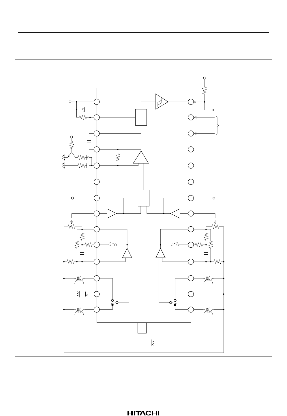
Block Diagram
HA12192F Series
HA12192F/HA1 2197F/HA12212F Series
CC
D V
CC
V
MSIMSG
MAOUT MSDET
V
(L)
DET
(L)
PBOUT
(L)
DIN
(L)
EQOUT
(L)
M-OUT
(L)
NFI
+
11121314151617192021222324 18
MS
DET
109876542128
MSOUT
F/R120/70
Micro computer
NR
+
MA
−
+
OFF/ON
BIAS
(R)
DET
(R)
PBOUT
(R)
DIN
(R)
EQOUT
(R)
M-OUT
(R)
NFI
I.A.
70µ
ON
Dolby B-NR
Decode only
−
+
LPF
Dolby B-NR
Decode only
70µ
−
+
I.A.
ON
3
RIN
RIP
FIN
(L)
(L)
2726
+
R
FR
F
25
RIN
V
FIN
(R)
REF
(R)
TAB
GND
Rev.5, Jun. 1999, page 7 of 89
HA12192F/HA1 2197F/HA12212F Series
HA12197F Series
CC
D V
CC
V
MSIMSG
MAOUT MSDET
V
NC
(L)
PBOUT
(L)
DIN
(L)
EQOUT
(L)
M-OUT
(L)
NFI
+
11121314151617192021222324 18
MS
DET
1098765421282726
MSOUTNCNC
F/R120/70
Micro computer
NC
+
I.A.
ON
70µ
−
+
MA
−
+
LPF
3
I.A.
ON
70µ
−
+
(R)
PBOUT
(R)
DIN
(R)
EQOUT
(R)
M-OUT
(R)
NFI
(L)
RIN
RIP
(L)
FIN
Rev.5, Jun. 1999, page 8 of 89
(R)
RIN
+
R
FR
F
25
V
FIN
REF
(R)
TAB
GND
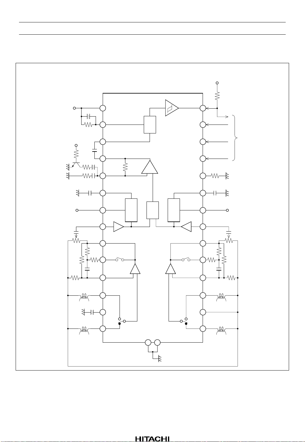
HA12212F
HA12192F/HA1 2197F/HA12212F Series
CC
D V
CC
V
MSIMSG
MAOUT MSDET
V
(L)
DET
(L)
PBOUT
(L)
DIN
(L)
EQOUT
(L)
M-OUT
(L)
NFI
+
17181920212223293031323334 28
MS
DET
1413121110982140
MSOUT
F/R120/70
Micro computer
NR
+
MA
−
+
OFF/ON
BIAS
(R)
DET
(R)
PBOUT
(R)
DIN
(R)
EQOUT
(R)
M-OUT
(R)
NFI
I.A.
70µ
ON
Dolby B-NR
Decode only
−
+
LPF
Dolby B-NR
Decode only
70µ
−
+
I.A.
ON
3
RIN
RIP
FIN
(L)
(L)
3938
+
R
FR
35
36
F
37
RIN
V
FIN
(R)
REF
(R)
Rev.5, Jun. 1999, page 9 of 89
HA12192F/HA1 2197F/HA12212F Series
Functional Description
Power Supply Range
HA12192F series and HA12197F series are provided with three line output level, which will permit on
optimum overload margin for power supply conditions. And these series are designed to operate on single
supply only.
Table 1 Spply Voltage Range
Product Single Supply
HA12192F, HA12197F 6.5V to 15.0V
HA12193F, HA12198F 6.8V to 15.0V
HA12194F, HA12199F 7.2V to 15.0V
Note: The lower limit of supply voltage depends on the line output reference level.
The minimum value of the overload margin is specified as 12dB by Dolby Laboratories.
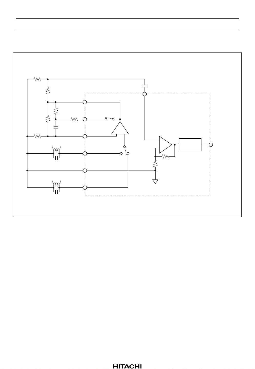
Reference Voltage
These devices provide the reference voltage of half the supply voltage that is the signal grounds. As the
peculiarity of these devices, the capacitor for the ripple filter is very small about 1/100 compared with their
usual value. The block diagram is shown as figure 1.
11
V
CC
23
RIP
+
C15
1µ
Note: HA12197F series is not built-in Dolby block.
: internal reference voltage
Figure 1 The Block Diagram of Reference Supply Voltage
+
−
+
−
+
−
+
−
MS block
26
V
REF
L, R channel
EQ block
L channel
Dolby block
R channel
Dolby block
Rev.5, Jun. 1999, page 10 of 89
HA12192F/HA1 2197F/HA12212F Series
Operating Mode Control
HA12192F series and HA12197F series provides fully electronic switching circuits. And each operating
mode control are controlled by parallel data (DC voltage).
Table 2 Threshold Voltage (V
Pin No. Lo Hi Unit Test Condition
7*1, 8, 9 –0.2 to 1.0 3.5 to 5.3 V
Table 3 Switching Truth Table
Pin No. Lo Hi
1
7*
8 120µ (NORMAL) 70µ (MATAL or CHROME)
9 FORWARD REVERSE
*1. Non connection regarding HA12197F series.
)
TH
NR-OFF NR-ON
Input Pin
Measure
V
Note: 1. Each pins are on pulled down with 100kΩ internal resistor. Therefore, it will be low-level when
each pins are open.
2. Over shoot level and under shoot level of input signal must be the standardi ze d.
(High: 5.3V, Low: –0.2V)
3. Reducing pop noise is so much better for 10kΩ to 22kΩ resistor and 1µF to 22µF capacitor
shown figure 2.
Input Pin
10 to 22kΩ
+
1 to 22µF
MPU
Figure 2 Interface for Reduction of Pop Noise
Rev.5, Jun. 1999, page 11 of 89
HA12192F/HA1 2197F/HA12212F Series
Input Block Diagram and Lev e l Diagram
PBOUT Level
HA12192F/HA12197F : 300mVrms
HA12193F/HA12198F : 387.5mVrms
HA12194F/HA12199F : 450mVrms
(−8.2dBs)
(−6.0dBs)
(−4.7dBs)
R6
5.1kΩ
R2
330kΩ
R1
180Ω
Note: 1. HA12197F series is not built-in Dolby B-NR.
R5
5.1kΩ
0.01µF
R4
12kΩ
C1
R3
18kΩ
EQ OUT
M-OUT
EQ Amp.
NFI
RIN
V
REF
FIN
−
Figure 3 Input Block Diagram
+
0.6mVrms
(−62.2dBs)
C2
0.1µF
DIN
30mVrms
(−28.2dBs)
Input Amp.
+
−
The each level shown above is typical value
when offering PBOUT level to PBOUT pin.
(EQ Amp. G
NR circuit
= 40dB, f=1kHz)
V
1
*
PBOUT
Adjustment of Playback Dolby Level
After replace R5 and R6 with a half-fix volume of 10kΩ, adjust playback Dolby level.
Rev.5, Jun. 1999, page 12 of 89
HA12192F/HA1 2197F/HA12212F Series
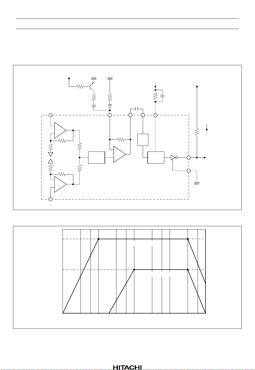
The Sensitivity Adjustment o f Music Sensor
Adjusting MS Amp. gain by external resistor, the sensitivity of music sensor can set up.
The music sensor block diagram is shown in figure 4, and frequency response is shown in figure 5.
DIN(L)
+
−
SER/REP
Input Amp.
REX2
2.7kΩ
CEX2
1µF
REP
mode
+
MSG
SER
mode
V
REX1
24kΩ
CEX1
0.01µF
90kΩ
−
−6dB
LPF
+
25kHz
−
+
Input Amp.
DIN(R)
Note: Input impedance of MSI is 100 kΩ typical.
Figure 4 Music Sensor Block Diagram
0.01µF
MA
OUT
MS Amp.
C8
330kΩ
MSI
ATT
R11
V
CC
DET
MS
DET
+
C6
0.33µF
MSOUT
GND
D V
CC
Micro
computer
I
L
R
L
G
[dB]
f
G
V2
V
G
V1
3
Repeat mode
f
1
Search mode (FF or REW)
10 100 1k 10k 25k 100k
f [Hz]
Figure 5 Frequency Response
Rev.5, Jun. 1999, page 13 of 89
f
4
f
2
HA12192F/HA1 2197F/HA12212F Series
Product GVIA ATT GVIA + ATT
HA12192F series 20dB 0dB 20dB
HA12197F 20dB 0dB 20dB
HA12198F 22.2dB –2.2dB 20dB
HA12199F 23.5dB –3.5dB 20dB
1. Search mode (FF or REW)
GV1=GVIA+ 20log 1 +
90k
REX1
+ATT [dB]
f1=
1
2π·CEX1·REX1
[Hz], f2=25k [Hz]
2. Repeat mode
GV2=GVIA+ 20log 1 +
REX1 ·REX2
Z=
REX1 +REX2
f3=
1
2π·CEX2·REX2
GVIA: Input Amp. GV = 20dB
90k
+ATT [dB],
Z
[Hz], f4=25k [Hz]
The sensitivity of music sensor (S) is computed by the formula mentioned below.
– 20log
130
30
*3
=12.7–GV[dB]
V2
S=–G
*1
V
Note: 1. Search mode: GV1, Repeat mode: G
*2
2. Standard level of DIN pin (Dolby level)
3. Standard sensing level of music sensor
Item REX1, 2 CEX1, 2 G
V1, 2
Search mode 24kΩ 0.01µF 33.5dB 663Hz 25kHz –14.8dB
Repeat mode 2.7kΩ 1µF 51.6dB 58.9Hz 25kHz –33.0dB
Note: S is 6dB down in case of one-side channel. And this MS presented hysteresis lest MSOUT terminal
should turn over again Hi level or Lo level, in case of thresh S level constantly.
f
1, 3
f
2, 4
S (one-side channel)
Rev.5, Jun. 1999, page 14 of 89
HA12192F/HA1 2197F/HA12212F Series
Music Sensor Time Constant
(1) Sensing no signal to signal (Attack) is determined by C6.
0.01µF to 1µF capacitor C6 can be applicable.
Sensing no signal to signal = C6 × 45000 (sec)
(2) Sensing signal to no signal (Recovery) is determined by C6 and R11, however preceding (1), 100kΩ to
1MΩ R11 can be applicable.
Sensing signal to no signal = C6 × R11 (sec)
Music Sensor Output (MSOUT)
As for the internal circuit of music sensor block, music sensor output pin is connected to the collector of
NPN type directly, therefore, output level will be “high” when sensing no signal. And output level will be
“low” when sensing signal.
Connection with microcomputer, design I
– MSOUTLo*
DV
CC
IL=
R
L
at 1mA Typ.
L
*MSOUTLo: Sensing signal (about 1V)
Note: Supply voltage of MSOUT pin must be less than V
voltage.
CC
The Tolerances of External Components for Dolby NR-Block (Only HA12192F Series)
For adequate Dolby NR tracking response, take external components shown below.
C10
0.1µF
±10%
16
DET(L)
HA12192F series
BIAS
65
R8
18kΩ
±2%
DET(R)
C4
0.1µF
±10%
Figure 6 Tolerance of External Components
Rev.5, Jun. 1999, page 15 of 89

HA12192F/HA1 2197F/HA12212F Series
Absolute Maximum Rating (Ta=25°C)
Item Symbol Rating Unit Note
Supply voltage V
Power dissipation Pd 400 mW Ta ≤ 85°C
Operating temperature Topr –40 to +85 °C
Storage temperature Tstg –55 to +125 °C
Max 16 V
CC
Rev.5, Jun. 1999, page 16 of 89
HA12192F/HA1 2197F/HA12212F Series
Electrical Characteristics HA12192F/HA12212F Series
(Ta = 25°C, PBOUT Level, 300mVrms(HA12192F/HA12212F), 387.5mVrms (HA12193F),
450mVrms(HA12194F), V
Item Symbol Min Typ Max Unit Test Condition Remark
Quiescent current I
Imput Amp. gain
(HA12192F/HA12212F)
Imput Amp. gain
(HA12193F)
Imput Amp. gain
(HA12194F)
B-type Decode boost DEC-2k (1) 2.8 4.3 5.8 dB Vout = –20dB, f = 2kHz
Signal handling Vo max 12.0 13.0 — dB THD = 1%, f = 1kHz *1
Signal to noise ratio S / N 70.0 80.0 — dB Rg = 5.1kΩ, CCIR / ARM
THD THD — 0.05 0.3 % Vin = 0dB, f = 1kHz
Channel separation CT RL (1) 65 80.0 — dB Vin = 10dB, f = 1kHz DIN IN
PB-EQ gain GV EQ 1k 37.0 40.0 43.0 dB Vin = 0.6mVrms, f = 1kHz 120µ
PB-EQ maximum output VoM 300 600 — mVrms THD = 1%, f = 1kHz *1
PB-EQ THD THD-EQ — 0.05 0.3 % Vin = 0.6mVrms, f = 1kHz
Noise voltage level
converted in input
MS sensing level V
MS output low level V
MS output leak current I
Control voltage V
Note: 1. VCC = 6.5V (HA12192F/HA12212F)
VCC = 6.8V (HA12193F)
VCC = 7.2V (HA12194F)
= 9.0V)
CC
Q
—9.5—mANR-ON, 70µ, No signal
GVIA 19.0 20.0 21.0 dB Vin = 0dB, f = 1kHz
GVIA 21.2 22.2 23.2
GVIA 22.5 23.5 24.5
DEC-2k (2) 7.0 8.5 10.0 Vout = –30dB, f = 2kHz
DEC-5k (1) 1.7 3.2 4.7 Vout = –20dB, f = 5kHz
DEC-5k (2) 6.7 8.2 9.7 Vout = –30dB, f = 5kHz
CT RL (2) 50 60.0 — EQ IN
GV EQ 10k(1) 33.0 36.0 39.0 Vin = 0.6mVrms, f = 10kHz
GV EQ 10k(2) 29.0 32.0 35.0 70µ
V
N
ON
OL
OH
IL
V
IH
—0.71.5µVrms Rg = 680Ω, DIN-AUDIO
–18.0 –14. 0 –10.0 dB f = 5kHz
—1.01.5V
—0.02.0µA
–0.2 — 1.0 V
3.5 — 5.3
Rev.5, Jun. 1999, page 17 of 89
HA12192F/HA1 2197F/HA12212F Series
Electrical Characteristics HA12197F Series
(Ta = 25°C, PBOUT Level, 300mVrms(HA12197F), 387.5mVrms(HA12198F), 450mVrms(HA12199F),
= 9.0V)
V
CC
Item Symbol Min Typ Max Unit Test Condition Remark
Quiescent current I
Imput Amp. gain
Q
GVIA 19.0 20.0 21.0 dB Vin = 0dB, f = 1kHz
(HA12197F)
Imput Amp. gain
GVIA 21.2 22.2 23.2
(HA12198F)
Imput Amp. gain
GVIA 22.5 23.5 24.5
(HA12199F)
Signal handling Vo max 12.0 13.0 — dB THD = 1%, f = 1kHz *1
Signal to noise ratio S / N 70.0 80.0 — dB Rg = 5.1kΩ, CCIR / ARM
THD THD — 0.05 0.3 % Vin = 0dB, f = 1kHz
Channel separation CT RL (1) 65 80.0 — dB Vin = 10dB, f = 1kHz DIN IN
CT RL (2) 50 60.0 — EQ IN
PB-EQ gain GV EQ 1k 37.0 40.0 43.0 dB Vin = 0.6mVrms, f = 1kHz 120µ
GV EQ 10k(1) 33.0 36.0 39.0 Vin = 0.6mVrms, f = 10kHz
GV EQ 10k(2) 29.0 32.0 35.0 70µ
PB-EQ maximum output VoM 300 600 — mVrms THD = 1%, f = 1kHz *1
PB-EQ THD THD-EQ — 0.05 0.3 % Vin = 0.6mVrms, f = 1kHz
Noise voltage level
V
N
converted in input
MS sensing level V
MS output low level V
MS output leak current I
Control voltage V
ON
OL
OH
IL
V
IH
Note: 1. VCC = 6.5V (HA12197F)
VCC = 6.8V (HA12198F)
V
= 7.2V (HA12199F)
CC
—4.77.1mA70µ, No signal
—0.71.5µVrms Rg = 680Ω, DIN-AUDIO
–18.0 –14. 0 –10.0 dB f = 5kHz
—1.01.5V
—0.02.0µA
–0.2 — 1.0 V
3.5 — 5.3
Rev.5, Jun. 1999, page 18 of 89
Test Circuit
HA12192F/HA12197F Series
HA12192F/HA1 2197F/HA12212F Series
NOISE METER
with CCIR/ARM filter
9V
5V
and DIN-AUDIO filter
EQ
PB
SW5
R25
10k
L
DC VM
SW10
SW8
EQ
MS
PB
R14
R18
R19
R
C9
R13
C20
5.1k
330k
180
10k
0.47µ
NOISE
R
PB
EQ
METER
SCOPE
OSCILLO
ANALYZER
DISTORTION
AC VM2
F
C18
70
8
120/70
RIN(R)
27
22µ
DC SOURCE3
ON
OFF
120
R9
22k
+
7
NR OFF/ON
NFI(R)
28
680
R23
C5
22µ
R8
18k
BIAS
C4
0.1µ
DET(R)
+
PBOUT(R)
C3
2.2µ
TAB
DIN(R)
D
3 456
EQOUT(R)
C2
R5
5.1k
0.1µ
2
M-OUT(R)
R4
12k
1
R3
18k
C1
0.01µ
+
R7
C19
10k
µ
0.47
R6
R2
R1
PB
5.1k
330k
180
SW9
EQ
L
R24
SW7
SW6
10k
DC SOURCE1
C7
100µ
+
330k
12
MSDET
RIP
23
1µ
+ +
C15
22µ
680
R21
+
C6
0.33µ
11
CC
V
FIN(L)
24
22µ
C16
C8
0.01µ
R11
13
14
0.01µ
24k
R12
V
C10
0.1µ
16 15
+
17
C11
2.2µ
TAB
+
D
18
C12
0.1µ
R15
5.1k
19
12k
R16
20
18k
R17
C13
0.01µ
MAOUT
MSG
DET(L)
DIN(L)
NFI(L)
21
R20
MSI
PBOUT(L)
EQOUT(L)
M-OUT(L)
RIN(L)
22
+
680
C14
DC SOURCE2
R
R10
3.9k
TAB
10
MSOUT
9
F/R
FP-28TB
HA12192F/HA12197F series
REF
V
FIN(R)
26
25
TAB
+
C17
+
680
R22
22µ
R
F
D
SW3
F
R
SW4
D
OFFON
RL
SW2
SW1
AC VM1 AUDIO SG
Resistor tolerance ±1%
Note: 1.
Capacitor tolerance ±1%
2.
Unit R: Ω C: F
3.
Rev.5, Jun. 1999, page 19 of 89

HA12192F/HA1 2197F/HA12212F Series
HA12212F
9V
5V
NOISE METER
with CCIR/ARM filter
and DIN-AUDIO filter
EQ
PB
SW5
R25
L
10k
DC VM
SW10
SW8
EQ
MS
PB
R14
R18
R19
R
330k
C9
R13
C20
5.1k
180
0.01µ
10k
0.47µ
NOISE
R
PB
EQ
METER
SCOPE
OSCILLO
ANALYZER
DISTORTION
AC VM2
F
70
12
120/70
RIN(R)
39
22µ
DC SOURCE3
ON
OFF
120
R9
22k
+
11
NR OFF/ON
NFI(R)
40
680
R23
C5
22µ
R8
18k
BIAS
C4
0.1µ
DET(R)
PBOUT(R)
+
R7
C3
NC
2.2µ
NC
NC
NC
4 5 6 7
DIN(R)
38910
EQOUT(R)
2
M-OUT(R)
1
µ
C19
0.47
+
D
C2
R5
5.1k
0.1µ
R4
12k
R3
18k
C1
0.01µ
10k
R6
R2
R1
PB
5.1k
330k
180
SW9
EQ
L
R24
SW7
SW6
10k
15
NC
MSOUT
FP-40B
HA12212F
FIN(R)
36 GND
+
22µ
C17
DC SOURCE2
R
R10
3.9k
13
14
F/R
REF
V
38
37
+
680
R22
C18
DC SOURCE1
C7
100µ
330k
22µ
+
18
MSDET
RIP
33
C15
1µ
R21
C6
680
17
34
+
0.33µ
V
FIN(L)
C16
16
CC
NC
35 GND
22µ
C8
0.01µ
R11
19
20
24k
R12
V
22 21
+
23
2.2µ
D
C12
R16
R17
C13
12k
18k
0.01µ
NC
NC
NC
NC
27 26 25 24
28
0.1µ
29
30
C11
+
R15
5.1k
MAOUT
MSG
DET(L)
DIN(L)
NFI(L)
31
R20
M-OUT(L)
MSI
PBOUT(L)
EQOUT(L)
RIN(L)
32
+
+ +
680
C14
Rev.5, Jun. 1999, page 20 of 89
R
F
D
SW3
F
SW4
R
D
OFFON
RL
SW2
SW1
AC VM1 AUDIO SG
Resistor tolerance ±1%
Note: 1.
Capacitor tolerance ±1%
2.
Unit R: Ω C: F
3.
Characteristic Curves
HA12192F Series
HA12192F/HA1 2197F/HA12212F Series
Quiescent Current vs. Supply
10
(mA)
CC
Quiescent Current I
Voltage (HA12192F/3F/4F)
9
8
No-Signal
NR-OFF (120/µ)
NR-OFF (70/µ)
NR-ON (120/µ)
NR-ON (70/µ)
7
6 8 10 12 14 16
Supply Voltage (V)
26
22
18
Gain (dB)
14
10
6
10 100 1 k 10 k 100 k 1 M
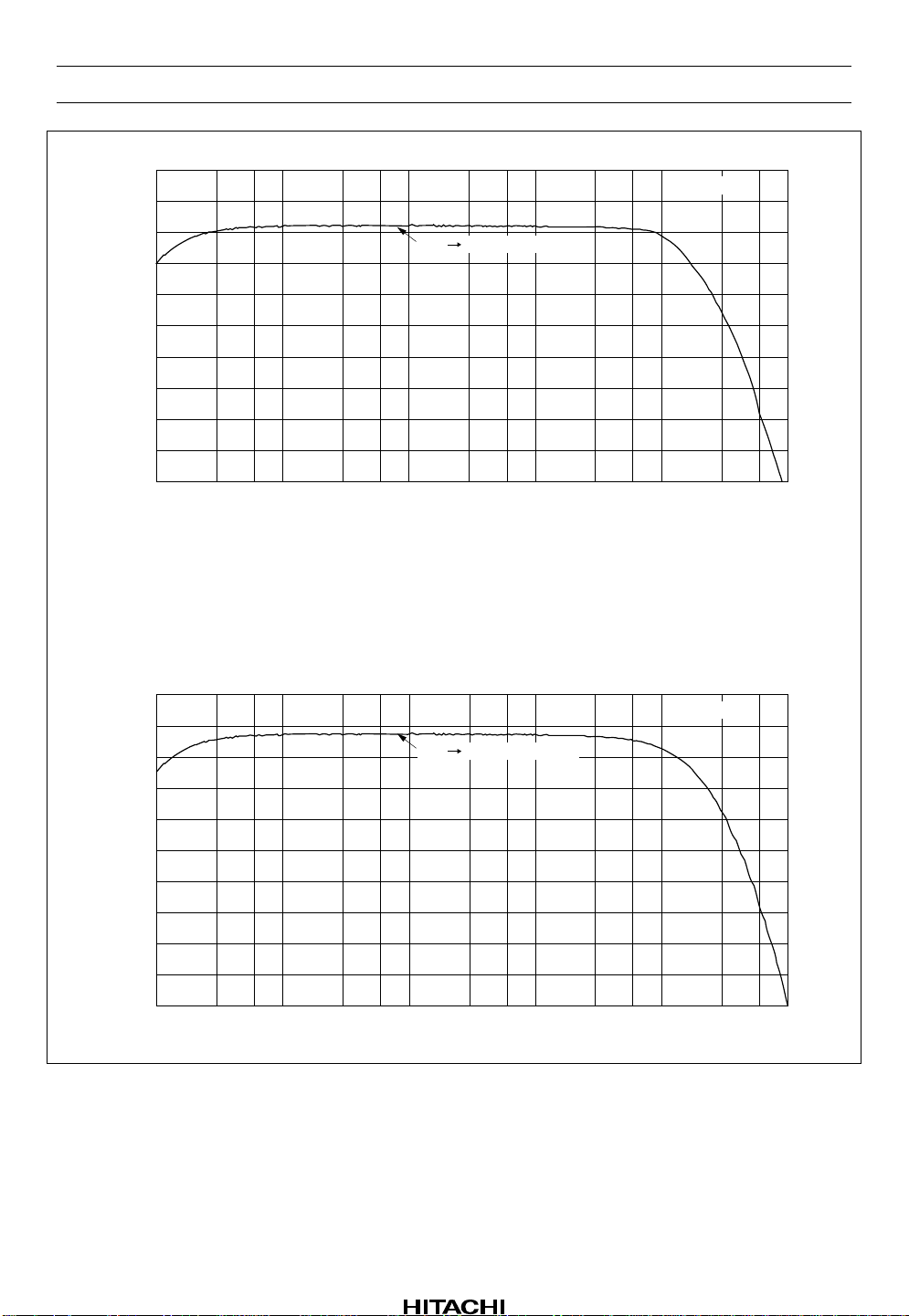
Input Amp Gain vs. Frequency (HA12192F)
VCC = 9 V
DIN PBout (NR-OFF)
Frequency (Hz)
Rev.5, Jun. 1999, page 21 of 89
HA12192F/HA1 2197F/HA12212F Series
26
22
18
Gain (dB)
14
10
6
10 100 1 k 10 k 100 k 1 M
26
DIN Input Amp. Gain vs. Frequency (HA12193F)
VCC = 9 V
DIN PBOUT, NR-OFF
Frequency (Hz)
DIN Input Amp. Gain vs. Frequency (HA12194F)
VCC = 9 V
22
18
Gain (dB)
14
10
6
10 100 1 k 10 k 100 k 1 M
DIN PBOUT, NR-OFF
Frequency (Hz)
Rev.5, Jun. 1999, page 22 of 89

–2
–4
HA12192F/HA1 2197F/HA12212F Series
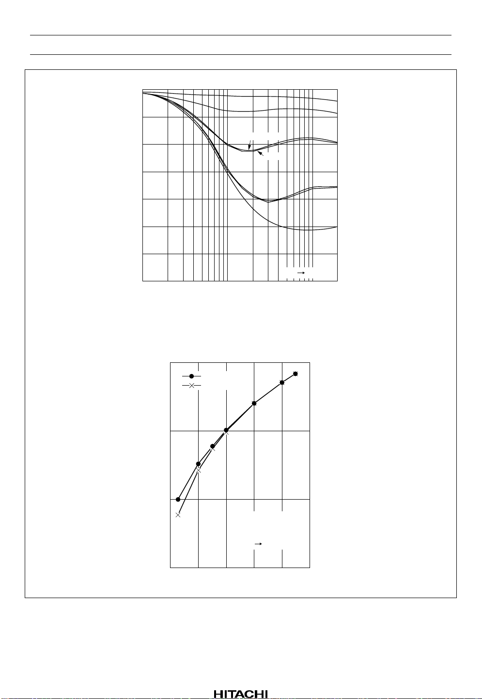
Decode Cut vs. Frequency (HA12192F)
0
VCC = 6.5 V, 9 V
Vout
0 dB
–10 dB
–20 dB
–6
–8
Decode Cut (dB)
–10
–12
–14
100 200 500 1 k 2 k 5 k 10 k 20 k
Frequency (Hz)
Decode Cut vs. Frequency (HA12193F)
0
–2
–4
–6
15 V
DIN PBOUT
VCC = 6.8 V, 9 V
15 V
–30 dB
–40 dB
Vout
0 dB
–10 dB
–20 dB
–8
Decode Cut (dB)
–10
–12
DIN PBOUT
–14
100 200 500 1 k 2 k 5 k 10 k 20 k
Frequency (Hz)
–30 dB
–40 dB
Rev.5, Jun. 1999, page 23 of 89
HA12192F/HA1 2197F/HA12212F Series
0
–2
–4
–6
–8
Decode Cut (dB)
–10
–12
–14
100 200 500 1 k 2 k 5 k 10 k 20 k
Decode Cut vs. Frequency (HA12194F)
VCC = 7.2 V, 9V
15 V
DIN PBOUT
Frequency (Hz)
Maximum Output Level
vs. Supply Voltage (HA12192F)
25
NR-OFF
NR-ON
Vout
0 dB
–10 dB
–20 dB
–30 dB
–40 dB
Rev.5, Jun. 1999, page 24 of 89
20
15
Maximum Output Level Vomax (dB)
10
6 8 10 12 14 16
Supply Voltage (V)
f = 1 kHz
0 dB = 300 mVrms
T.H.D. = 1.0%
DIN PBout
HA12192F/HA1 2197F/HA12212F Series
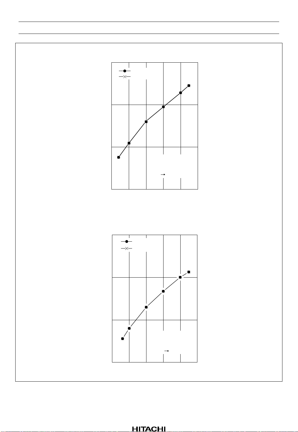
Maximum Output Level
vs. Supply Voltage (HA12193F)
25
NR-OFF
NR-ON
20
15
Maximum Output Level Vomax (dB)
10
6 8 10 12 14 16
Supply Voltage (V)
Maximum Output Level
vs. Supply Voltage (HA12194F)
25
20
15
f = 1 kHz
0 dB = 387.5 mVrms
T.H.D. = 1.0%
DIN PBout
NR-OFF
NR-ON
Maximum Output Level Vomax (dB)
10
6 8 10 12 14 16
Supply Voltage (V)
f = 1 kHz
Vout = 450 mVrms
T.H.D = 1.0 %
DIN PBOUT
Rev.5, Jun. 1999, page 25 of 89

HA12192F/HA1 2197F/HA12212F Series
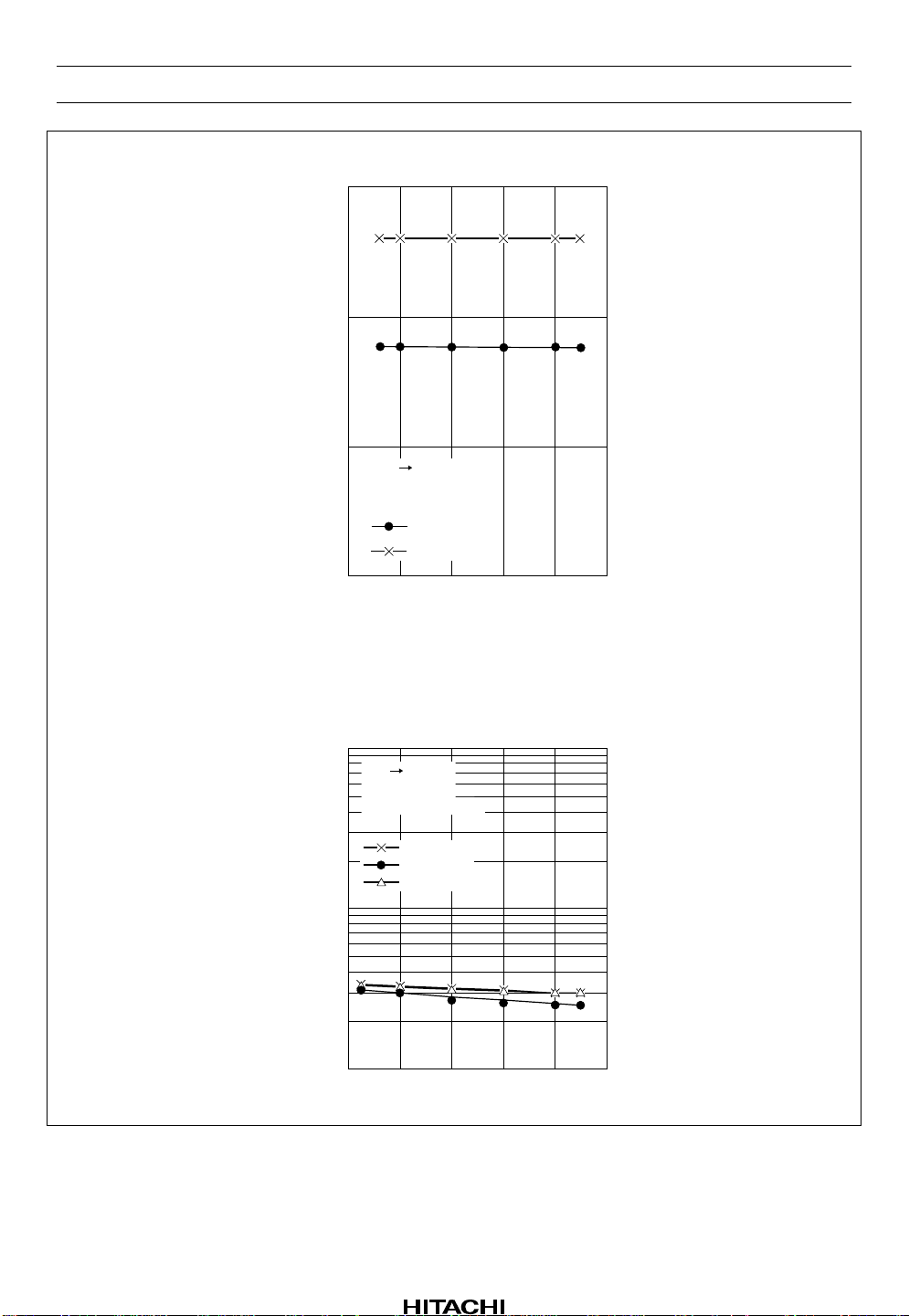
Signal to Noise Ratio
vs. Supply Voltage (HA12192F)
85
80
75
Signal to Noise Ratio S/N (dB)
DIN PBout
CCIR/ARM
S = 300 mVrms
NR-OFF
NR-ON
70
6 8 10 12 14 16
Supply Voltage (V)
Signal to Noise Ratio
vs. Supply Voltage (HA12193F)
85
80
75
Signal to Noise Ratio S/N (dB)
DIN PBout
CCIR/ARM
S = 387.5 mVrms
NR-OFF
NR-ON
70
6 8 10 12 14 16
Supply Voltage (V)
Rev.5, Jun. 1999, page 26 of 89
HA12192F/HA1 2197F/HA12212F Series
Signal to Noise Ratio
vs. Supply Voltage (HA12194F)
85
80
75
Signal to Noise Ratio S/N (dB)
DIN PBOUT
CCIR/ARM
S = 450 mVrms
NR-OFF
NR-ON
70
6 8 10 12 14 16
Supply Voltage (V)
Total Harmonic Distortion vs.
Supply Voltage (1) (HA12192F)
1.0
DIN PBout
NR-OFF
Vout = 300 mVrms
f = 100 Hz
f = 1 kHz
f = 10 kHz
0.1
Total Harmonic Distortion T.H.D. (%)
0.01
6 8 10 12 14 16
Supply Voltage (V)
Rev.5, Jun. 1999, page 27 of 89
 Loading...