


ANPEC APL1117-VC-TU, APL1117-VC-TR, APL1117-UC-TU, APL1117-UC-TR, APL1117-33FC-TR Datasheet
...APL1117
1A Low Dropout Fast Response Positive Adjustable Regulator and Fixed 1.8V, 2.5V, 2.85V and 3.3V
Features
•Guaranteed Output Voltage Accuracy within 2%
•Fast Transient Response
•Guaranteed Dropout Voltage at Multiple Currents
•Load Regulation : 0.1% Typ.
•Line Regulation : 0.03% Typ.
•Low Dropout Voltage : 1.1V Typ. at IOUT =1A
•Current Limit : 1A Typ. at TJ=25° C
•On-Chip Thermal Limiting : 150° C Typ.
•Adjustable Output : 1.25~10.7V
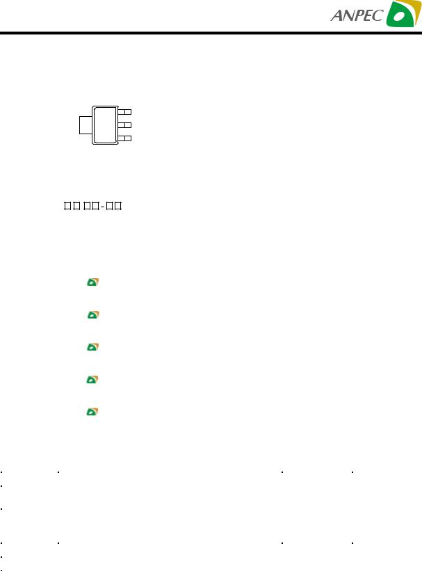
•Standard 3-pin TO-220, TO-252, TO-263 and SOT-223 Power Packages
General Description
The APL1117 is a low dropout three-terminal adjustable regulators with 1A output current capability. In order to obtain lower dropout voltage and faster transient response, which is critical for low voltage applications , the APL1117 has been optimized. The device is available in an adjustable version and fixed output voltages of 1.8V, 2.5V, 2.85V and 3.3V. The output available voltage range of an adjustable version is from 1.25~10.7V with an input supply below 12V. Dropout voltage is guaranteed at a maximum of 1.3V at 1A. Current limit is trimmed to ensure specified output current and controlled short-circuit current. On-chip thermal limiting provides protection against any combination of overload that would create excessive junction temperatures. The APL1117 is available in the industry standard 3-pin TO-220, TO-252, TO263, and the low profile surface mount SOT-223 power packages which can be used in applications where space is limited.
Applications |
Pin Description |
|
||||
• |
Active SCSI Terminators |
|
|
Front View for TO-220 |
|
|
• Low Voltage Logic Supplies |
|
|
|
|
||
|
|
3 |
|
VIN |
||
|
|
|
||||
|
|
|
||||
• |
Battery-Powered Circuitry |
|
|
2 |
|
VOUT |
|
|
|
||||
|
|
|
||||
• Post Regulator for Switching Power Supply |
|
|
1 |
|
ADJ/GND |
|
|
|
|
||||
|
|
|
||||
Front View for TO-263
|
|
3 |
|
|
VIN |
|
|
|
|
||
TAB is V |
OUT |
2 |
|
|
VOUT |
|
|
||||
|
|
||||
|
|
1 |
|
|
ADJ/GND |
|
|
|
|
||
|
|
|
|
||
|
|
|
|
|
|
Front View for TO-252
|
3 |
VIN |
TAB IS VOUT |
2 |
V |
|
|
OUT |
|
1 |
ADJ/GND |
|
|
ANPEC reserves the right to make changes to improve reliability or manufacturability without notice, and advise customers to obtain the latest version of relevant information to verify before placing orders.
Copyright ANPEC Electronics Corp. |
1 |
www.anpec.com.tw |
Rev. B.8 - Jun., 2003 |
|
|
APL1117
Pin Description (Cont.)
Front View for SOT-223
T A B IS V O U T |
|
3 |
IN |
|
|||
2 |
O U T |
||
|
1 |
A D J /G N D |
|
Ordering and Marking Information
A P L 1 1 1 7 - |
|
|
|
|
|
|
|
|
|
|
|
|
P a c k a g e C o d e |
|
|
|
|
|||||
|
|
|
|
|
|
|
|
|
|
|
|
F : T O -2 2 0 |
G : T O -2 6 3 |
U : T O -2 5 2 |
V : S O T -2 2 3 |
|||||||
|
|
|
|
|
|
|
|
|
|
|
|
|
|
|
|
|
|
|||||
|
|
|
|
|
|
|
|
|
|
|
|
|
|
|
|
|
H a n d lin g C o d e |
T e m p . R a n g e |
|
|
|
|
|
|
|
|
|
|
|
|
|
|
|
|
|
|
|
|
|
C : 0 to 7 0 ° C |
|
|
|
|
|
|
|
|
|
|
|
|
|
|
|
|
|
|
|
|
|
|
|
|
|
|||
|
|
|
|
|
|
|
|
|
|
|
|
|
|
|
|
|
T e m p . R a n g e |
H a n d lin g C o d e |
|
|
|
|
|
|
|
|
|
|
|
|
|
|
|
|
|
|
|
|
|
T U : T u b e |
T R : T a p e & R e e l |
|
|||
|
|
|
|
|
|
|
|
|
|
|
|
|
|
|
|
|
P a c k a g e C o d e |
|
||||
|
|
|
|
|
|
|
|
|
|
|
|
|
|
|
|
|
V o lta g e C o d e |
|
|
|
|
|
|
|
|
|
|
|
|
|
|
|
|
|
|
|
|
|
|
|
|
|
|||
|
|
|
|
|
|
|
|
|
|
|
|
|
|
|
|
|
|
|
|
|
|
|
|
|
|
|
|
|
|
|
|
|
|
|
|
|
|
|
|
V o lta g e C o d e |
1 8 : 1 .8 V |
2 5 : 2 .5 V |
2 8 : 2 .8 5 V |
3 3 : 3 .3 V |
|
|
|
|
|
|
|
|
|
|
|
|
|
|
|
|
|
|
|
B la n k : A d ju s ta b le V e rs io n |
|
|
||
|
|
|
|
|
|
|
|
|
|
|
|
|
|
|
|
|
|
|
|
|
|
|
A P L 1 1 1 7 F /G /U : |
|
|
|
|
|
|
|
|
|
|
X X X X X - D a te C o d e |
A P L 1 1 1 7 V : |
|
A P L 1 1 1 7 |
X X X X X - D a te C o d e |
|||||||
|
A P L 1 1 1 7 |
|
|
X X X X X |
||||||||||||||||||
|
|
|
|
|
|
|
|
|
|
|
|
|
|
|||||||||
|
|
|
|
|
|
X X X X X |
|
|
|
|
|
|
|
|
|
|||||||
|
|
|
|
|
|
|
|
|
|
|
|
|
|
|
||||||||
|
|
|
|
|
|
|
|
|
|
|
|
|
|
|
|
|
|
|
|
|
|
|
|
|
|
|
|
|
|
|
|
|
|
|
|
|
|
|
|||||||
A P L 1 1 1 7 -1 8 F /G /U : |
|
1 8 |
|
X X X X X - D a te C o d e |
A P L 1 1 1 7 -1 8 V : |
|
A P L 1 1 1 7 |
X X X X X - D a te C o d e |
||||||||||||||
|
A P L 1 1 1 7 |
|
|
X X X X X 1 8 |
||||||||||||||||||
|
|
|
|
|
|
|
|
|
|
|
|
|
|
|||||||||
|
|
|
|
|
|
X X X X X |
|
|
|
|
|
|
|
|
|
|||||||
|
|
|
|
|
|
|
|
|
|
|
|
|
|
|
||||||||
|
|
|
|
|
|
|
|
|
|
|
|
|
|
|
|
|
|
|
|
|
|
|
|
|
|
|
|
|
|
|
|
|
|
|
|
|
|
|
|
|
|
|
|
|
|
|
|
|
|
|
|
2 5 |
|
|
|
|
|
|
|
|
|
|||||||
A P L 1 1 1 7 -2 5 F /G /U : |
|
|
X X X X X - D a te C o d e |
A P L 1 1 1 7 -2 5 V : |
|
A P L 1 1 1 7 |
X X X X X - D a te C o d e |
|||||||||||||||
A P L 1 1 1 7 |
|
|
||||||||||||||||||||
|
|
X X X X X 2 5 |
||||||||||||||||||||
|
|
|
|
|
|
X X X X X |
|
|
|
|
|
|
|
|
||||||||
|
|
|
|
|
|
|
|
|
|
|
|
|
|
|
|
|||||||
|
|
|
|
|
|
|
|
|
|
|
|
|
|
|
|
|||||||
|
|
|
|
|
|
|
|
|
|
|
|
|
|
|
|
|||||||
|
|
|
|
|
|
2 8 |
|
|
|
|
|
|
|
|
|
|||||||
A P L 1 1 1 7 -2 8 F /G /U : |
|
|
|
X X X X X - D a te C o d e |
A P L 1 1 1 7 -2 8 V : |
|
A P L 1 1 1 7 |
X X X X X - D a te C o d e |
||||||||||||||
|
|
|
|
|
|
|
|
|
|
|
|
|||||||||||
|
A P L 1 1 1 7 |
|
|
X X X X X 2 8 |
||||||||||||||||||
|
|
|
|
|
|
|
|
|
|
|
|
|
|
|||||||||
|
|
|
|
|
|
X X X X X |
|
|
|
|
|
|
|
|
|
|||||||
|
|
|
|
|
|
|
|
|
|
|
|
|
|
|
||||||||
|
|
|
|
|
|
|
|
|
|
|
|
|
|
|
|
|
|
|
|
|
|
|
|
|
|
|
|
|
|
|
|
|
|
|
|
|
|
|
|||||||
|
|
|
|
|
|
3 3 |
|
|
|
|
|
|
|
|
|
|||||||
A P L 1 1 1 7 -3 3 F /G /U : |
|
|
X X X X X - D a te C o d e |
A P L 1 1 1 7 -3 3 V : |
|
A P L 1 1 1 7 |
X X X X X - D a te C o d e |
|||||||||||||||
A P L 1 1 1 7 |
|
|
||||||||||||||||||||
|
|
X X X X X 3 3 |
||||||||||||||||||||
|
|
|
|
|
|
X X X X X |
|
|
|
|
|
|
|
|
||||||||
|
|
|
|
|
|
|
|
|
|
|
|
|
|
|
||||||||
|
|
|
|
|
|
|
|
|
|
|
|
|
|
|
|
|
|
|
|
|
|
|
Absolute Maximum Ratings
Symbol |
|
Parameter |
Rating(Note) |
|
Unit |
VI |
Input Voltage |
APL1117, APL1117-33 |
15 |
|
V |
|
APL1117-18, APL1117-25, APL1117-28 |
9 |
|
|
|
|
|
|
|
|
|
TJ |
Operating Junction Temperature Range |
|
|
° C |
|
|
|
Control Section |
0 to 125 |
|
|
|
|
Power Transistor |
0 to 150 |
|
|
TSTG |
Storage Temperature Range |
-65 to +150 |
|
° C |
|
TL |
Lead Temperature (Soldering, 10 second) |
260 |
|
° C |
|
Note : The values here show the absolute maximum rating, and for normal usage please refer the test condition in Electrical |
|||||
Characteristics Table. |
|
|
|
|
|
|
|
|
|
|
|
Copyright ANPEC Electronics Corp. |
2 |
|
www.anpec.com.tw |
||
Rev. B.8 - Jun., 2003 |
|
|
|
|
|

APL1117
Electrical Characteristics (Cont.)
|
Symbol |
Parameter |
|
Test Conditions |
APL1117 |
Unit |
|||||||
|
|
|
|
|
|
|
|
|
|
Min. |
Typ. |
Max. |
|
|
VREF |
Reference Voltage |
10mA≤ |
IOUT ≤ 1A, 1.4V≤ (VIN -VOUT) ≤ 10.75V, |
1.225 |
1.250 |
1.275 |
V |
|||||
|
|
|
|
TJ =0~125° C |
|
|
|
|
|
||||
|
|
|
|
|
|
|
|
|
|
|
|
||
|
|
|
|
|
|
|
|
|
|
|
|
|
|
|
VOUT |
Output Voltage |
|
|
|
|
|
|
|
|
|
|
|
|
|
|
APL1117-18 |
TJ =0~125° C, |
|
|
|
|
|
|
|
||
|
|
|
|
0≤ IOUT≤ |
1.5A, 3.5V≤ VIN≤ 9V, |
1.764 |
1.800 |
1.836 |
|
||||
|
|
|
APL1117-25 |
TJ =0~125° C, |
|
|
|
|
|
|
|
||
|
|
|
|
0≤ IOUT≤ |
1A, 4V≤ VIN≤ 9V, |
2.450 |
2.500 |
2.550 |
V |
||||
|
|
|
APL1117-28 |
TJ =0~125° C, |
|
|
|
|
|
|
|||
|
|
|
|
|
|
|
|
|
|||||
|
|
|
|
|
|
|
|
|
|
||||
|
|
|
|
0≤ IOUT≤ |
1A, 4.25V≤ VIN≤ 9V, |
2.790 |
2.850 |
2.910 |
|
||||
|
|
|
APL1117-33 |
TJ =0~125° C, |
|
|
|
|
|
|
|
||
|
|
|
|
0≤ IOUT≤ |
1A, 4.75V≤ |
|
VIN≤ 12V, |
3.235 |
3.300 |
3.365 |
|
||
|
|
|
|
|
|
|
|
|
|
|
|
|
|
|
REGLINE |
Line Regulation |
IOUT=10mA, 1.5V≤ (VIN -VOUT )≤ 10.75V (Note1) |
|
|
|
|
||||||
|
|
|
APL1117 |
|
0.03 |
0.2 |
% |
||||||
|
|
|
APL1117-18 |
IOUT=0A, 3.5V≤ VIN≤ 9V (Note1) |
|
1 |
6 |
mV |
|||||
|
|
|
APL1117-25 |
IOUT=0A, 4V≤ VIN≤ 5.5V (Note1) |
|
1 |
6 |
|
|||||
|
|
|
APL1117-28 |
IOUT=0A, 4.25V≤ |
VIN ≤ |
5.15V (Note1) |
|
1 |
6 |
|
|||
|
|
|
APL1117-33 |
IOUT=0A, 4.75V≤ |
VIN ≤ |
7.75V (Note1) |
|
1 |
6 |
|
|||
|
REGLOAD |
Load Regulation |
(VIN -VOUT)=3V, 0≤ IOUT ≤ 1A (Note1) |
|
|
|
|
||||||
|
|
|
APL1117 |
|
0.1 |
0.4 |
% |
||||||
|
|
|
APL1117-18 |
VIN=3.5V, 0≤ |
IOUT ≤ 1A (Note1) |
|
1 |
10 |
mV |
||||
|
|
|
APL1117-25 |
VIN =4V, 0≤ IOUT ≤ 1A (Note1) |
|
1 |
10 |
|
|||||
|
|
|
APL1117-28 |
VIN=4.25V, 0≤ |
IOUT ≤ |
1A (Note1) |
|
1 |
10 |
|
|||
|
|
|
APL1117-33 |
VIN=4.75V, 0≤ |
IOUT ≤ |
1A (Note1) |
|
1 |
10 |
|
|||
|
VD |
Dropout Voltage |
IOUT=100mA (Note2) |
|
|
|
1 |
1.1 |
|
||||
|
|
|
|
IOUT=500mA (Note2) |
|
|
|
1.05 |
1.2 |
V |
|||
|
|
|
|
IOUT=1A (Note2) |
|
|
|
|
|
1.1 |
1.3 |
|
|
|
ILIMIT |
Current Limit |
(VIN -VOUT)=5V, TJ=25° C |
1000 |
|
|
mA |
||||||
|
IADJ |
Adjust Pin Current |
(VIN -VOUT)=3V, IOUT=10mA |
|
60 |
120 |
A |
||||||
|
|
|
APL1117 |
|
|
|
|
|
|
|
|
|
|
|
|
|
|
|
|
|
|
|
|
|
|
||
|
∆ IADJ |
Adjust |
Pin Current |
10mA≤ |
IOUT ≤ 1A, |
|
|
|
0.2 |
5 |
A |
||
|
|
Change APL1117 |
1.4V≤ (VIN -VOUT) ≤ 10.75V |
|
|
|
|
||||||
|
IO |
Minimum Load |
(VIN -VOUT)=10.75V (Note3) |
|
1.7 |
|
mA |
||||||
|
|
Current |
APL1117 |
|
|
|
|
|
|
|
|
|
|
|
PSRR |
Ripple Rejection |
fRIPPLE=120Hz, VRIPPLE=1VP-P, |
60 |
75 |
|
dB |
||||||
|
|
|
|
(VIN -VOUT)=3V |
|
|
|
|
|
|
|
||
|
TR |
Thermal Regulation |
TJ=25° C, 30ms Pulse |
|
0.01 |
0.02 |
%/ W |
||||||
|
TS |
Temperature |
|
|
|
|
|
|
|
0.5 |
|
% |
|
|
|
Stability |
|
|
|
|
|
|
|
|
|
|
|
|
LS |
Long -Term |
TJ =125° C,1000Hrs. |
|
0.3 |
|
% |
||||||
|
|
Stability |
|
|
|
|
|
|
|
|
|
|
|
|
|
|
|
|
|
|
|
|
|
|
|
|
|
Copyright ANPEC Electronics Corp. |
|
|
3 |
|
|
www.anpec.com.tw |
|||||||
Rev. B.8 - Jun., 2003 |
|
|
|
|
|
|
|
|
|
|
|
||

APL1117
Electrical Characteristics (Cont.)
Symbol |
Parameter |
Test Conditions |
APL1117 |
|
Unit |
||
Min. |
Typ. |
Max. |
|||||
VN |
RMS Output Noise |
TJ=25° C,10Hz≤ F≤ 10kHz, (% of VOUT) |
|
0.003 |
|
|
% |
|
|
|
|
|
|
|
|
θ th |
Thermal Resistance |
Junction to Case, at Tab |
|
15 |
|
|
° C/ W |
|
|
Junction to Ambient |
|
50 |
|
|
|
OT |
Over Temperature |
|
|
150 |
|
|
° C |
|
Point |
|
|
|
|
|
|
IQ |
Quiescent Current |
|
|
|
|
|
|
|
APL1117-18 |
VIN≤ 9V |
|
5.5 |
|
10 |
mA |
|
APL1117-25 |
VIN≤ 9V |
|
5.5 |
|
10 |
|
|
APL1117-28 |
VIN≤ 9V |
|
5.5 |
|
10 |
|
|
APL1117-33 |
VIN≤ 12V |
|
5.5 |
|
10 |
|
Note 1 : See thermal regulation specifications for changes in output voltage due to heating effects. Load line regulations are measured at a constant junction temperature by low duty cycle pulse testing.
Note 2 : Dropout voltage is specified over the full output current range of the device. Dropout voltage is defined as the minimum input/output differential measured at the specified output current. Test points and limits are also shown on the Dropout Voltage curve.
Note 3 : Minimum load current is defined as the minimum output current required to maintain regulation.
Copyright ANPEC Electronics Corp. |
4 |
www.anpec.com.tw |
Rev. B.8 - Jun., 2003 |
|
|
APL1117
Application Circuits
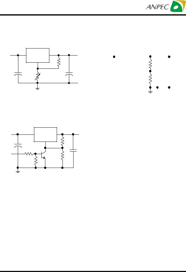
1.25V to 10.7V Adjustable Regulator
|
|
APL1117 |
|
|
|
|
|
VIN |
|
IN |
OUT |
|
|
V |
|
|
|
|
|
R1 |
|
|
OUT1 |
|
|
ADJ |
|
|
|
||
|
|
|
|
|
|
||
|
|
|
|
121Ω |
|
|
|
+ 10µ |
F |
|
|
+ 100µ |
F |
||
|
C1* |
R2 |
|
|
C2 |
|
|
|
|
|
1k |
|
|
|
|
* Needed if device is far from filter capacitors |
|
|
|||||
|
VOUT = 1.250V X R1 + R2 |
|
|
||||
|
|
|
|
|
R1 |
|
|
|
5V Regulator with Shutdown |
|
|
||||
|
|
APL1117 |
|
|
|
||
VIN |
|
IN |
|
OUT |
121Ω |
5V |
|
+ |
|
|
ADJ |
|
|
||
10µ |
F |
|
|
1% |
|
|
|
|
|
|
+ |
|
|
||
|
|
1k |
|
|
100µ |
F |
|
TTL |
|
|
|
365Ω |
|||
|
|
|
|
|
|
||
|
|
1k |
|
1% |
|
|
|
|
|
|
|
|
|
||
Improving Ripple Rejection
|
|
|
|
|
|
|
|
|
|
|
APL1117 |
|
|
|
|
|
|
|
|
|
|
|
||
VIN |
|
|
|
|
|
|
|
|
|
|
IN |
|
OUT |
|
|
|
|
|
|
|
|
V |
|
|
|
+ |
|
|
|
|
|
|
R1 |
|
|
|
OUT |
||||||||||||
|
|
|
|
|
|
|
|
|
ADJ |
|
|
|
|
|
|
|
||||||||
|
|
|
|
|
|
|
|
|
121Ω |
|
|
|
|
|
|
|
||||||||
1 0 µ |
F |
|
|
|
|
|
|
|
|
|
|
|
|
|
|
|
|
|||||||
|
|
|
|
|
|
|
|
|
|
|
|
|
|
|
1% |
|
|
|
|
150µ F |
||||
|
|
|
|
|
|
|
|
|
|
|
|
|
|
|
|
|
|
|
|
|
|
|||
|
|
|
|
|
|
|
|
|
|
|
|
|
|
|
|
|
|
|
|
|
|
|||
|
|
|
|
|
|
|
|
|
|
|
|
|
R2 |
|
+ |
|
|
C1 |
|
|
|
|
|
|
|
|
|
|
|
|
|
|
|
|
|
|
|
365Ω |
|
|
|
|
1 0 µ |
F |
|
|
|
|
|
|
|
|
|
|
|
|
|
|
|
|
|
1% |
|
|
|
|
|
|
|
|
|
|
||
|
|
|
|
|
|
|
|
|
|
|
|
|
|
|
|
|
|
|
|
|
|
|
|
|
* C1 improves ripple rejection. XC should be approximately equal to R1 at ripple frequency
Copyright ANPEC Electronics Corp. |
5 |
www.anpec.com.tw |
Rev. B.8 - Jun., 2003 |
|
|

APL1117
Typical Characteristics
Load Transietn Response |
Line Transient Response |
|
5 |
|
|
|
|
APL1117-33 |
0.02 |
|
6 |
|
|
|
|
|
|
|
|
|
|
|
|
|
4.5 |
|
|
|
|
|
|
|
|
|
|
4 |
|
|
|
|
|
|
0.01 |
|
5 |
Output Current (A) |
3.5 |
|
|
|
|
|
|
|
Input Voltage (V) |
4 |
3 |
|
|
|
|
|
|
0 |
|||
|
|
|
|
|
|
|
||||
2.5 |
CIN=10 F |
|
|
|
|
|
3 |
|||
|
|
|
|
|
|
|||||
2 |
|
|
|
|
-0.01 |
|
||||
COUT=10 |
F Tantalum |
|
|
|
||||||
1.5 |
VIN=5V |
|
|
|
|
|
2 |
|||
|
|
|
|
|
|
|
||||
1 |
|
|
|
|
|
|
-0.02 |
|
||
|
|
|
|
|
|
|
|
1 |
||
|
0.5 |
|
|
|
|
|
|
|
|
|
|
|
|
|
|
|
|
|
|
|
|
|
0 |
|
|
|
|
|
|
-0.03 |
|
0 |
|
-100 |
100 |
300 |
500 |
700 |
900 |
|
|
||
|
|
|
|
APL1117-33 |
0.15 |
|
|
|
|
|
0.1 |
|
CIN=10 F |
|
|
|
|
|
COUT=10 |
F Tantalum |
|
|
|
|
IOUT=0.1A |
|
|
0.05 |
|
|
|
|
|
|
0 |
|
|
|
|
|
-0.05 |
-20 |
30 |
80 |
130 |
180 |
|
Time ( S) |
Time ( S) |
Dropout Voltage vs. Output Current
|
1.25 |
|
|
|
|
APL1117-33 |
|
|
|
|
|
|
|
|
1.2 |
|
|
|
|
|
(V) |
1.15 |
|
|
|
|
|
Voltage |
1.1 |
|
|
|
|
|
|
|
|
|
|
|
|
Dropout |
1.05 |
|
|
|
|
|
1 |
|
|
|
|
|
|
|
|
|
|
|
|
|
|
0.95 |
|
|
|
|
|
|
0.9 |
|
|
|
|
|
|
0 |
0.2 |
0.4 |
0.6 |
0.8 |
1 |
Output Voltage vs. Input Voltage
|
3.5 |
|
|
|
|
|
|
|
|
|
|
3 |
|
|
|
|
|
|
|
|
|
(V) |
2.5 |
|
|
|
|
|
|
|
|
|
|
|
|
|
|
|
|
|
|
|
|
Voltage |
2 |
|
|
|
|
|
|
|
|
|
1.5 |
|
|
|
|
|
|
|
|
|
|
Output |
|
|
|
|
|
|
|
|
|
|
1 |
|
|
|
|
|
|
|
|
|
|
|
|
|
|
|
|
|
|
|
|
|
|
0.5 |
|
|
|
|
|
|
|
|
|
|
0 |
|
|
|
|
|
|
|
|
|
|
0 |
1 |
2 |
3 |
4 |
5 |
6 |
7 |
8 |
9 |
Output Current (A) |
Input Voltage (V) |
Copyright ANPEC Electronics Corp. |
6 |
www.anpec.com.tw |
Rev. B.8 - Jun., 2003 |
|
|
 Loading...