


AMD MACH210AQ-20JC, MACH210AQ-15JC, MACH210AQ-12JC, MACH210A-7VC, MACH210A-7JC Datasheet
...FINAL |
COM'L: -7/10/12/15/20, Q-12/15/20 IND: -12/14/18/24 |
|
MACH210A-7/10/12
MACH210-12/15/20
MACH210AQ-12/15/20
High-Density EE CMOS Programmable Logic
Advanced
Micro
Devices
DISTINCTIVE CHARACTERISTICS
44 Pins
64 Macrocells
7.5 ns tPD Commercial
12 ns tPD Industrial
133 MHz fCNT
38 Inputs; 210A Inputs have built-in pull-up resistors
Peripheral Component Interconnect (PCI) compliant
32 Outputs
64 Flip-flops; 2 clock choices
4 “PAL22V16” blocks with buried macrocells
Pin-compatible with MACH110, MACH111, MACH211, and MACH215
GENERAL DESCRIPTION
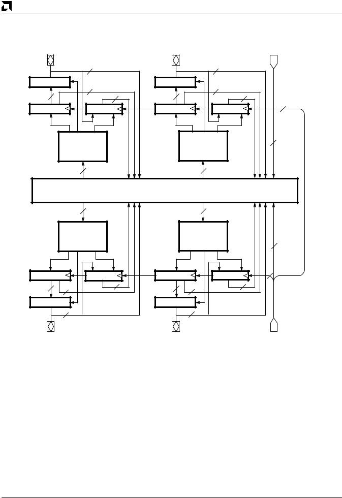
The MACH210 is a member of AMD's high-performance EE CMOS MACH 2 device family. This device has approximately six times the logic macrocell capability of the popular PAL22V10 without loss of speed.
The MACH210 consists of four PAL blocks interconnected by a programmable switch matrix. The four PAL blocks are essentially “PAL22V16” structures complete with product-term arrays and programmable macrocells, including additional buried macrocells. The switch matrix connects the PAL blocks to each other and to all input pins, providing a high degree of connectivity between the fully-connected PAL blocks. This allows designs to be placed and routed efficiently.
The MACH210 has two kinds of macrocell: output and buried. The MACH210 output macrocell provides regis-
tered, latched, or combinatorial outputs with programmable polarity. If a registered configuration is chosen, the register can be configured as D-type or T-type to help reduce the number of product terms. The register type decision can be made by the designer or by the software. All output macrocells can be connected to an I/O cell. If a buried macrocell is desired, the internal feedback path from the macrocell can be used, which frees up the I/O pin for use as an input.
The MACH210 has dedicated buried macrocells which, in addition to the capabilities of the output macrocell, also provide input registers or latches for use in synchronizing signals and reducing setup time requirements.
Publication# 14128 Rev. I Amendment /0
Issue Date: May 1995
AMD
BLOCK DIAGRAM
|
|
|
|
I0–I 1, |
|
I/O0–I/O 7 |
|
I/O8–I/O 15 |
|
I3–I 4 |
|
|
8 |
|
8 |
|
|
I/O Cells |
8 |
I/O Cells |
8 |
|
|
|
|
|
|||
8 |
8 |
8 |
8 |
|
|
Macrocells |
Macrocells |
Macrocells |
Macrocells |
2 |
|
|
|||||
|
OE |
|
OE |
|
|
|
44 x 68 |
|
44 x 68 |
4 |
|
AND Logic Array |
AND Logic Array |
||||
|
|||||
|
and |
|
and |
|
|
Logic Allocator |
Logic Allocator |
|
|||
|
22 |
|
22 |
|
|
Switch Matrix
|
|
22 |
|
|
22 |
|
|
|
44 x 68 |
|
|
44 x 68 |
|
|
AND Logic Array |
|
AND Logic Array |
|
||
|
|
and |
|
|
and |
2 |
|
Logic Allocator |
|
Logic Allocator |
|||
|
|
|
||||
|
|
OE |
|
|
OE |
|
Macrocells |
Macrocells |
Macrocells |
Macrocells |
2 |
||
|
||||||
8 |
8 |
8 |
8 |
8 |
8 |
|
|
|
|
|
|
||
I/O Cells |
|
I/O Cells |
|
|
||
|
8 |
|
|
8 |
|
|
I/O24–I/O 31 |
|
I/O16–I/O 23 |
|
CLK0/I2, |
||
|
|
|
|
|
|
CLK1/I5 |
|
|
|
|
|
|
14128I-1 |
2 |
MACH210-7/10/12/15/20, Q-12/15/20 |
AMD 
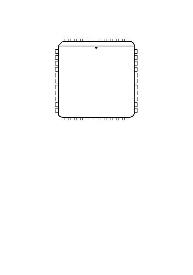
CONNECTION DIAGRAM
Top View
|
|
|
|
|
PLCC |
|
|
|
|
|
||
|
4 |
3 |
2 |
1 |
0 |
GND |
CC |
31 |
30 |
29 |
28 |
|
|
I/O |
I/O |
I/O |
I/O |
I/O |
V |
I/O |
I/O |
I/O |
I/O |
|
|
|
6 |
5 |
4 |
3 |
2 |
1 |
44 |
43 42 |
41 |
40 |
|
|
I/O5 |
7 |
|
|
|
|
|
|
|
|
|
39 |
I/O27 |
|
|
|
|
|
|
|
|
|
|
|||
I/O6 |
8 |
|
|
|
|
|
|
|
|
|
38 |
I/O26 |
I/O7 |
9 |
|
|
|
|
|
|
|
|
|
37 |
I/O25 |
I0 |
10 |
|
|
|
|
|
|
|
|
|
36 |
I/O24 |
I1 |
11 |
|
|
|
|
|
|
|
|
|
35 |
CLK1/I5 |
GND |
12 |
|
|
|
|
|
|
|
|
|
34 |
GND |
CLK0/I2 |
13 |
|
|
|
|
|
|
|
|
|
33 |
I4 |
I/O8 |
14 |
|
|
|
|
|
|
|
|
|
32 |
I3 |
I/O9 |
15 |
|
|
|
|
|
|
|
|
|
31 |
I/O23 |
I/O10 |
16 |
|
|
|
|
|
|
|
|
|
30 |
I/O22 |
I/O11 |
17 |
|
20 |
21 22 |
23 |
24 |
25 |
26 |
|
29 |
I/O21 |
|
|
18 19 |
27 28 |
|
|||||||||
|
12 |
13 |
14 |
15 |
CC |
GND |
16 |
17 |
18 |
19 |
20 |
|
|
I/O |
I/O |
I/O |
I/O |
V |
I/O |
I/O |
I/O |
I/O |
I/O |
|
|
|
|
|
|
|
|
|
|
|
|
|
|
14128I-2 |
Note:
Pin-compatible with MACH110, MACH111, MACH211, and MACH215.
MACH210-7/10/12/15/20, Q-12/15/20 |
3 |
AMD
CONNECTION DIAGRAM
Top View
TQFP
|
|
|
|
I/O4 |
I/O3 |
I/O2 |
I/O1 |
I/O0 |
GND |
V |
I/O31 |
I/O30 |
I/O29 |
I/O28 |
|
|
|||||||||||||||||
|
|
|
|
|
|
|
|
|
|
|
|
|
|
|
|
|
|
|
CC |
|
|
|
|
|
|
|
|
|
|
|
|
|
|
|
|
|
|
|
|
|
|
|
|
|
|
|
|
|
|
|
|
|
|
|
|
|
|
|
|
|
|
|
|
|
|
|
|
|
|
|
|
|
|
|
|
|
|
|
|
|
|
|
|
|
|
|
|
|
|
|
|
|
|
|
|
|
|
|
|
|
|
|
|
|
|
|
|
|
|
|
|
|
|
|
|
|
|
|
|
|
|
|
|
|
|
|
|
|
|
|
|
|
|
|
|
|
|
|
|
44 |
43 |
42 |
41 |
40 |
39 |
38 |
37 |
36 |
35 |
34 |
|
|
|
|
|||||||||||||||
|
|
|
|
|
|
||||||||||||||||||||||||||||
I/O5 |
|
|
|
1 |
|
|
|
|
|
|
|
|
|
|
|
|
|
|
|
|
|
|
|
|
|
|
33 |
|
|
|
I/O27 |
||
|
|
|
|
|
|
|
|
|
|
|
|
|
|
|
|
|
|
|
|
|
|
|
|
|
|
|
|||||||
I/O6 |
|
|
|
2 |
|
|
|
|
|
|
|
|
|
|
|
|
|
|
|
|
|
|
|
|
|
|
32 |
|
|
|
I/O26 |
||
|
|
|
|
|
|
|
|
|
|
|
|
|
|
|
|
|
|
|
|
|
|
|
|
|
|
|
|||||||
I/O7 |
|
|
|
3 |
|
|
|
|
|
|
|
|
|
|
|
|
|
|
|
|
|
|
|
|
|
|
31 |
|
|
|
I/O25 |
||
|
|
|
|
|
|
|
|
|
|
|
|
|
|
|
|
|
|
|
|
|
|
|
|
|
|
|
|||||||
|
|
|
|
|
|
|
|
|
|
|
|
|
|
|
|
|
|
|
|
|
|
|
|
|
|
|
|||||||
I0 |
|
|
|
4 |
|
|
|
|
|
|
|
|
|
|
|
|
|
|
|
|
|
|
|
|
|
|
30 |
|
|
|
I/O24 |
||
|
|
|
|
|
|
|
|
|
|
|
|
|
|
|
|
|
|
|
|
|
|
|
|
|
|
|
|||||||
|
|
|
|
|
|
|
|
|
|
|
|
|
|
|
|
|
|
|
|
|
|
|
|
|
|
|
|||||||
I1 |
|
|
|
5 |
|
|
|
|
|
|
|
|
|
|
|
|
|
|
|
|
|
|
|
|
|
|
29 |
|
|
|
CLK1/I5 |
||
|
|
|
|
|
|
|
|
|
|
|
|
|
|
|
|
|
|
|
|
|
|
|
|
|
|
|
|||||||
GND |
|
|
|
6 |
|
|
|
|
|
|
|
|
|
|
|
|
|
|
|
|
|
|
|
|
|
|
28 |
|
|
|
GND |
||
|
|
|
|
|
|
|
|
|
|
|
|
|
|
|
|
|
|
|
|
|
|
|
|
|
|
|
|||||||
|
|
|
|
|
|
|
|
|
|
|
|
|
|
|
|
|
|
|
|
|
|
|
|
|
|
|
|||||||
CLK0/I2 |
|
|
|
7 |
|
|
|
|
|
|
|
|
|
|
|
|
|
|
|
|
|
|
|
|
|
|
27 |
|
|
|
I4 |
||
|
|
|
|
|
|
|
|
|
|
|
|
|
|
|
|
|
|
|
|
|
|
|
|
|
|
|
|||||||
I/O8 |
|
|
|
8 |
|
|
|
|
|
|
|
|
|
|
|
|
|
|
|
|
|
|
|
|
|
|
26 |
|
|
|
I3 |
||
|
|
|
|
|
|
|
|
|
|
|
|
|
|
|
|
|
|
|
|
|
|
|
|
|
|
|
|||||||
I/O9 |
|
|
|
9 |
|
|
|
|
|
|
|
|
|
|
|
|
|
|
|
|
|
|
|
|
|
|
25 |
|
|
|
I/O23 |
||
|
|
|
|
|
|
|
|
|
|
|
|
|
|
|
|
|
|
|
|
|
|
|
|
|
|
|
|||||||
I/O10 |
|
|
|
10 |
|
|
|
|
|
|
|
|
|
|
|
|
|
|
|
|
|
|
|
|
|
|
24 |
|
|
|
I/O22 |
||
|
|
|
|
|
|
|
|
|
|
|
|
|
|
|
|
|
|
|
|
|
|
|
|
|
|
|
|||||||
I/O11 |
|
|
|
11 |
|
|
|
|
|
|
|
|
|
|
|
|
|
|
|
|
|
|
|
|
|
|
23 |
|
|
|
I/O21 |
||
|
|
|
|
|
|
|
|
|
|
|
|
|
|
|
|
|
|
|
|
|
|
|
|
|
|
|
|||||||
|
|
|
|
|
|
|
|
|
|
|
|
|
|
|
|
|
|
|
|
|
|
|
|
|
|
|
|||||||
|
|
|
|
12 |
13 |
|
14 |
15 |
16 |
|
17 |
18 |
|
19 |
20 |
21 |
22 |
|
|
|
|
|
|||||||||||
|
|
|
|
|
|
|
|
|
|
|
|
|
|
|
|
|
|
|
|
|
|
|
|
|
|
|
|
|
|
|
|
|
|
|
|
|
|
|
|
|
|
|
|
|
|
|
|
|
|
|
|
|
|
|
|
|
|
|
|
|
|
|
|
|
|
|
|
|
|
|
|
I/O12 |
I/O13 |
I/O14 |
I/O15 |
V |
GND |
I/O16 |
I/O17 |
I/O18 |
I/O19 |
I/O20 |
|
|
|||||||||||||||||
|
|
|
|
|
|
|
|
|
|
|
|
|
|
CC |
|
|
|
|
|
|
|
|
|
|
|
|
|
|
|
|
|
|
|
14128I-3
Note:
Pin-compatible with MACH111 and MACH211.
PIN DESIGNATIONS
CLK/I = Clock or Input
GND = Ground
I = Input
I/O = Input/Output
VCC = Supply Voltage
4 |
MACH210-7/10/12/15/20, Q-12/15/20 |
AMD 
ORDERING INFORMATION
Commercial Products
AMD programmable logic products for commercial applications are available with several ordering options. The order number (Valid Combination) is formed by a combination of:
MACH 210A -7 J C
FAMILY TYPE
MACH = Macro Array CMOS High-Speed
DEVICE NUMBER
210 = 64 Macrocells, 44 Pins
210A = 64 Macrocells, 44 Pins, Input Pull-Up Resistors 210AQ = 64 Macrocells, 44 Pins, Input Pull-Up Resistors,
Quarter Power
SPEED
-7 = 7.5 ns tPD -10 = 10 ns tPD -12 = 12 ns tPD -15 = 15 ns tPD -20 = 20 ns tPD
OPTIONAL PROCESSING
Blank = Standard Processing
OPERATING CONDITIONS
C = Commercial (0°C to +70°C)
PACKAGE TYPE
J = 44-Pin Plastic Leaded Chip
Carrier (PL 044)
V= 44-Pin Thin Quad Flat Pack (PQT044)
Valid Combinations
MACH210A-7
JC, MACH210A-10 VC
MACH210A-12
MACH210-12
MACH210-15
MACH210-20
JC
MACH210AQ-12
MACH210AQ-15
MACH210AQ-20
Valid Combinations
The Valid Combinations table lists configurations planned to be supported in volume for this device. Consult the local AMD sales office to confirm availability of specific valid combinations or to check on newly released combinations.
MACH210-7/10/12/15/20, Q-12/15/20 (Com'l) |
5 |

AMD
ORDERING INFORMATION
Industrial Products
AMD programmable logic products for industrial applications are available with several ordering options. The order number (Valid Combination) is formed by a combination of:
|
|
|
|
|
|
|
|
|
|
MACH |
210A -12 |
J |
I |
|||||||||||||||||
FAMILY TYPE |
|
|
|
|
|
|
|
|
|
|
|
|
|
|
|
|
|
|
|
|
|
|
|
|
|
OPTIONAL PROCESSING |
||||
|
|
|
|
|
|
|
|
|
|
|
|
|
|
|
|
|
|
|
|
|
|
|
|
|
||||||
MACH = |
Macro Array CMOS High-Speed |
|
|
|
|
|
|
|
|
|
|
|
|
|
|
|
|
|
Blank = Standard Processing |
|||||||||||
DEVICE NUMBER |
|
|
|
|
|
|
|
|
|
|
|
|
|
|
|
|
|
|
|
|
|
|
|
|
|
|||||
|
|
|
|
|
|
|
|
|
|
|
|
|
|
|
|
|
|
|
|
|
|
|
|
|
||||||
210 |
|
= |
64 Macrocells, 44 Pins |
|
|
|
|
|
|
|
|
|
|
|
|
|
|
|
|
|
|
|
|
|
|
OPERATING CONDITIONS |
||||
210A |
= |
64 Macrocells, 44 Pins, Input Pull-Up Resistors |
|
|
|
|
|
|
|
|
|
|
|
|
|
|
|
|
|
|||||||||||
|
|
|
|
|
|
|
|
|
|
|
|
|
|
|
|
|
I = Industrial (–40 °C to +85°C) |
|||||||||||||
|
|
|
|
|
|
|
|
|
|
|
|
|
|
|
|
|
|
|
|
|
|
|
|
|
|
|
|
|
|
|
SPEED |
|
|
|
|
|
|
|
|
|
|
|
|
|
|
|
|
|
|
|
|
|
|
|
|
|
|
|
PACKAGE TYPE |
||
|
|
|
|
|
|
|
|
|
|
|
|
|
|
|
|
|
|
|
|
|
|
|
|
|
|
|
||||
-12 |
= |
12 ns tPD |
|
|
|
|
|
|
|
|
|
|
|
|
|
|
|
|
|
|
|
|
|
|
J = 44-Pin Plastic Leaded Chip |
|||||
|
|
|
|
|
|
|
|
|
|
|
|
|
|
|
|
|
|
|
|
|
|
Carrier (PL 044) |
||||||||
-14 |
= |
14.5 ns tPD |
|
|
|
|
|
|
|
|
|
|
|
|
|
|
|
|
|
|
|
|
|
|
||||||
|
|
|
|
|
|
|
|
|
|
|
|
|
|
|
|
|
|
|
|
|
|
|
||||||||
-18 |
= |
18 ns tPD |
|
|
|
|
|
|
|
|
|
|
|
|
|
|
|
|
|
|
|
|
|
|
|
|||||
-24 |
= |
24 ns tPD |
|
|
|
|
|
|
|
|
|
|
|
|
|
|
|
|
|
|
|
|
|
|
|
|||||
|
|
|
|
|
|
|
|
|
|
|
|
|
|
|
|
|
|
|
|
Valid Combinations |
||||||||||
|
|
|
|
Valid Combinations |
|
|
|
|
|
|
|
|
|
|
|
|
|
|
|
|
|
|||||||||
|
|
|
|
MACH210A-12 |
|
|
|
|
|
|
|
|
|
|
|
The |
Valid |
Combinations table lists configurations |
||||||||||||
|
|
|
|
|
|
|
|
|
|
|
|
|
|
|
planned to be supported in volume for this device. Con- |
|||||||||||||||
|
|
|
|
MACH210A-14 |
|
|
|
|
|
|
|
|
|
|
|
|||||||||||||||
|
|
|
|
|
|
|
|
|
|
|
|
|
|
|
sult the local AMD sales office to confirm availability of |
|||||||||||||||
|
|
|
|
MACH210-14 |
|
JI |
|
|
|
|
|
|
|
|
|
specific valid combinations or to check on newly re- |
||||||||||||||
|
|
|
|
|
|
|
|
|
|
|
|
|
|
|
|
|
|
leased combinations. |
||||||||||||
|
|
|
|
MACH210-18 |
|
|
|
|
|
|
|
|
|
|
|
|||||||||||||||
|
|
|
|
|
|
|
|
|
|
|
|
|
|
|
|
|
|
|
|
|
|
|
|
|
|
|
|
|||
|
|
|
|
MACH210-24 |
|
|
|
|
|
|
|
|
|
|
|
|
|
|
|
|
|
|
|
|
|
|
|
|
||
6 |
MACH210-12/14/18/24 (Ind) |

|
|
|
|
|
|
AMD |
|
||
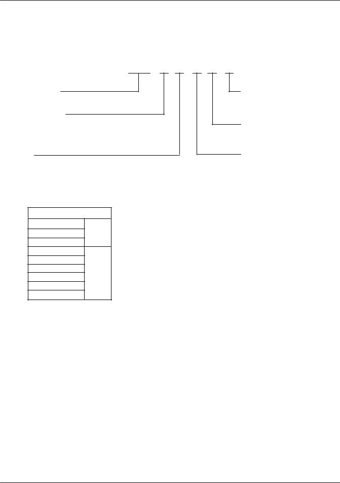
FUNCTIONAL DESCRIPTION |
Table 1 illustrates which product term clusters are |
||||||||
The MACH210 consists of four PAL blocks connected |
available to each macrocell within a PAL block. Refer to |
||||||||
Figure 1 for cluster and macrocell numbers. |
|||||||||
by a switch matrix. There are 32 I/O pins and 4 |
|||||||||
|
|
|
|
|
|
|
|
||
dedicated input pins feeding the switch matrix. These |
|
Table 1. Logic Allocation |
|||||||
signals are distributed to the four PAL blocks for efficient |
|
||||||||
|
|
|
|
|
|
|
|
||
design implementation. There are two clock pins that |
|
Macrocell |
|
Available |
|
|
|||
can also be used as dedicated inputs. |
|
Output |
|
Buried |
|
Clusters |
|
|
|
The MACH210A inputs and I/O pins have built-in pull-up |
|
M0 |
|
|
|
C0, C1, C2 |
|
|
|
resistors. While it is always a good design practice to tie |
|
|
|
M1 |
|
C0, C1, C2, C3 |
|
||
unused pins high, the 210A pull-up resistors provide |
|
|
|
|
|
|
|
|
|
|
M2 |
|
|
|
C1, C2, C3, C4 |
|
|
||
design security and stability in the event that unused |
|
|
|
|
|
||||
|
|
|
M3 |
|
C2, C3, C4, C5 |
|
|||
pins are left disconnected. |
|
|
|
|
|
|
|
|
|
|
M4 |
|
|
|
C3, C4, C5, C6 |
|
|
||
|
|
|
|
|
|
||||
The PAL Blocks |
|
|
|
M5 |
|
C4, C5, C6, C7 |
|
||
|
|
|
|
|
|
|
|
||
|
M6 |
|
|
|
C5, C6, C7, C8 |
|
|
||
Each PAL block in the MACH210 (Figure 1) contains a |
|
|
|
|
|
||||
|
|
|
M7 |
|
C6, C7, C8, C9 |
|
|
||
64-product-term logic array, a logic allocator, 8 output |
|
|
|
|
|
||||
|
|
|
|
|
|
|
|
||
|
M8 |
|
|
|
C7, C8, C9, C10 |
|
|
||
macrocells, 8 buried macrocells, and 8 I/O cells. The |
|
|
|
|
|
||||
|
|
|
M9 |
|
C8, C9, C10, C11 |
|
|
||
switch matrix feeds each PAL block with 22 inputs. This |
|
|
|
|
|
||||
|
M10 |
|
|
|
C9, C10, C11, C12 |
|
|
||
makes the PAL block look effectively like an independ- |
|
|
|
|
|
||||
ent “PAL22V16” with 8 buried macrocells. |
|
|
|
M11 |
|
C10, C11, C12, C13 |
|
||
In addition to the logic product terms, two output enable |
|
M12 |
|
|
|
C11, C12, C13, C14 |
|
|
|
|
|
|
M13 |
|
C12, C13, C14, C15 |
|
|
||
product terms, an asynchronous reset product term, |
|
|
|
|
|
||||
|
M14 |
|
|
|
C13, C14, C15 |
|
|
||
and an asynchronous preset product term are provided. |
|
|
|
|
|
||||
One of the two output enable product terms can be |
|
|
|
M15 |
|
C14, C15 |
|
||
chosen within each I/O cell in the PAL block. All flip-flops |
|
|
|
|
|
|
|
|
|
within the PAL block are initialized together. |
The Macrocell |
|
|
|
|
|
|||
|
|
|
|
|
|
||||
The Switch Matrix |
The MACH210 has two types of macrocell: output and |
||||||||
The MACH210 switch matrix is fed by the inputs and |
buried. The output macrocells can be configured as |
||||||||
either registered, latched, or combinatorial, with pro- |
|||||||||
feedback signals from the PAL blocks. Each PAL block |
|||||||||
grammable polarity. The macrocell provides internal |
|||||||||
provides 16 internal feedback signals and 8 I/O |
|||||||||
feedback whether configured with or without the flip- |
|||||||||
feedback signals. The switch matrix distributes these |
|||||||||
flop. The registers |
can be |
configured as D-type or |
|||||||
signals back to the PAL blocks in an efficient manner |
|||||||||
T-type, allowing for product-term optimization. |
|||||||||
that also provides for high performance. The design |
|||||||||
|
|
|
|
|
|
|
|
||
software automatically configures the switch matrix |
The flip-flops can individually select one of two clock/ |
||||||||
when fitting a design into the device. |
gate pins, which are also available as data inputs. The |
||||||||
The Product-term Array |
registers are clocked on the LOW-to-HIGH transition of |
||||||||
the clock signal. The latch holds its data when the gate |
|||||||||
The MACH210 product-term array consists of 64 |
input is HIGH, and is transparent when the gate input is |
||||||||
product terms for logic use, and 4 special-purpose |
LOW. The flip-flops can also be asynchronously initial- |
||||||||
product terms. Two of the special-purpose product |
ized with the common asynchronous reset and preset |
||||||||
terms provide programmable output enable; one pro- |
product terms. |
|
|
|
|
|
|||
vides asynchronous reset, and one provides asynchro- |
The buried macrocells are the same as the output |
||||||||
nous preset. |
macrocells if they are used for generating logic. In that |
||||||||
The Logic Allocator |
case, the only thing that distinguishes them from the |
||||||||
output macrocells is the fact that there is no I/O cell |
|||||||||
|
|||||||||
The logic allocator in the MACH210 takes the 64 logic |
connection, and the signal is only used internally. The |
||||||||
product terms and allocates them to the 16 macrocells |
buried macrocell can also be configured as an input |
||||||||
as needed. Each macrocell can be driven by up to 16 |
register or latch. |
|
|
|
|
|
|||
product terms. The design software automatically |
|
|
|
|
|
|
|
|
|
configures the logic allocator when fitting the design into the device.
MACH210-7/10/12/15/20, Q-12/15/20 |
7 |

AMD
The I/O Cell
The I/O cell in the MACH210 consists of a three-state output buffer. The three-state buffer can be configured in one of three ways: always enabled, always disabled, or controlled by a product term. If product term control is chosen, one of two product terms may be used to provide the control. The two product terms that are available are common to all I/O cells in a PAL block.
These choices make it possible to use the macrocell as an output, an input, a bidirectional pin, or a three-state output for use in driving a bus.
PCI Compliance
The MACH210A-7/10 is fully compliant with the PCI Local Bus Specification published by the PCI Special Interest Group. The MACH210A-7/10's predictable timing ensures compliance with the PCI AC specifications independent of the design. On the other hand, in CPLD and FPGA architectures without predictable timing, PCI compliance is dependent upon routing and product term distribution.
8 |
MACH210-7/10/12/15/20, Q-12/15/20 |

AMD 
0 |
4 |
8 |
12 |
16 |
20 |
24 |
28 |
32 |
36 |
40 |
43 |
Output Enable
Output Enable
Asynchronous Reset
Asynchronous Preset
|
|
|
|
|
|
|
|
|
|
|
|
|
|
|
|
I/O |
I/O |
|
|
|
|
|
|
|
|
|
|
|
|
|
|
|
Output |
Cell |
|
|
|
|
|
|
|
|
|
|
|
|
|
|
|
|
|
||
|
|
|
|
|
|
|
|
|
|
|
|
|
M0 |
|
|
||
|
|
|
|
|
|
|
|
|
|
|
|
|
Macro |
|
|
||
|
|
|
|
|
|
|
|
|
|
|
|
|
cell |
|
|
||
|
|
|
|
|
|
|
|
|
|
|
|
|
|
|
2 |
|
|
|
|
|
|
|
|
|
|
|
|
|
|
|
|
|
Buried |
|
|
|
|
|
|
|
|
|
|
|
|
|
|
|
M1 |
Macro |
|
|
|
|
|
|
|
|
|
|
|
|
|
|
|
|
cell |
|
|
||
|
|
|
|
|
|
|
|
|
|
|
|
|
|
|
2 |
|
|
|
|
|
|
|
|
|
|
|
|
|
|
|
|
|
|
I/O |
I/O |
|
|
|
|
|
|
|
|
|
|
|
|
|
|
|
Output |
Cell |
|
|
|
|
|
|
|
|
|
|
|
|
|
|
M2 |
|
|
||
|
|
|
|
|
|
|
|
|
|
|
|
|
Macro |
|
|
||
|
|
|
|
|
|
|
|
|
|
|
|
|
cell |
|
|
||
|
|
|
|
|
|
|
|
|
|
|
|
|
|
|
2 |
|
|
|
|
|
|
|
|
|
|
|
|
|
|
|
M3 |
Buried |
|
|
|
|
|
|
|
|
|
|
|
|
|
|
|
|
Macro |
|
|
||
|
|
|
|
|
|
|
|
|
|
|
|
|
cell |
|
|
||
0 |
|
|
|
|
|
|
|
|
|
|
|
|
|
|
2 |
|
|
|
|
|
|
|
|
|
|
|
|
C0 |
|
|
|
|
|
|
|
|
|
|
|
|
|
|
|
|
|
|
|
|
|
|
I/O |
I/O |
|
|
|
|
|
|
|
|
|
|
|
|
|
|
|
|
Output |
Cell |
|
|
|
|
|
|
|
|
|
|
|
|
C1 |
|
M4 |
|
|
||
|
|
|
|
|
|
|
|
|
|
|
|
Macro |
|
|
|||
|
|
|
|
|
|
|
|
|
|
|
|
cell |
|
|
|||
|
|
|
|
|
|
|
|
|
|
|
|
|
|
|
2 |
|
|
|
|
|
|
|
|
|
|
|
|
|
C2 |
|
|
|
|
|
|
|
|
|
|
|
|
|
|
|
|
|
C3 |
|
M5 |
Buried |
|
|
|
|
|
|
|
|
|
|
|
|
|
|
|
Macro |
|
|
|||
|
|
|
|
|
|
|
|
|
|
|
|
cell |
|
|
|||
|
|
|
|
|
|
|
|
|
|
|
|
|
|
|
2 |
|
|
|
|
|
|
|
|
|
|
|
|
|
C4 |
|
|
|
|
I/O |
I/O |
|
|
|
|
|
|
|
|
|
|
|
|
Allocator |
|
|
|
Cell |
|
|
|
|
|
|
|
|
|
|
|
|
C5 |
M6 |
Output |
|
|
||
|
|
|
|
|
|
|
|
|
|
|
Macro |
|
|
||||
|
|
|
|
|
|
|
|
|
|
|
cell |
|
|
||||
|
|
|
|
|
|
|
|
|
|
|
|
|
|
2 |
|
|
|
|
|
|
|
|
|
|
|
|
|
|
C6 |
|
|
|
|
|
|
Switch |
|
|
|
|
|
|
|
|
|
|
C7 |
M7 |
Buried |
|
|
||
|
|
|
|
|
|
|
|
|
|
Logic |
Macro |
|
|
||||
Matrix |
|
|
|
|
|
|
|
|
|
|
cell |
|
|
||||
|
|
|
|
|
|
|
|
|
|
|
|
|
|
2 |
|
|
|
|
|
|
|
|
|
|
|
|
|
|
C8 |
|
|
|
I/O |
I/O |
|
|
|
|
|
|
|
|
|
|
|
|
|
|
|
|
Output |
Cell |
|
|
|
|
|
|
|
|
|
|
|
|
C9 |
|
M8 |
|
|
||
|
|
|
|
|
|
|
|
|
|
|
|
Macro |
|
|
|||
|
|
|
|
|
|
|
|
|
|
|
|
cell |
|
|
|||
|
|
|
|
|
|
|
|
|
|
|
|
|
|
|
2 |
|
|
|
|
|
|
|
|
|
|
|
|
|
C10 |
|
|
|
|
|
|
|
|
|
|
|
|
|
|
|
|
|
C11 |
|
M9 |
Buried |
|
|
|
|
|
|
|
|
|
|
|
|
|
|
|
Macro |
|
|
|||
|
|
|
|
|
|
|
|
|
|
|
|
cell |
|
|
|||
|
|
|
|
|
|
|
|
|
|
|
|
|
|
|
2 |
|
|
|
|
|
|
|
|
|
|
|
|
|
C12 |
|
|
|
|
I/O |
I/O |
|
|
|
|
|
|
|
|
|
|
|
|
|
|
|
|
Cell |
|
|
|
|
|
|
|
|
|
|
|
|
C13 |
|
M10 |
Output |
|
||
|
|
|
|
|
|
|
|
|
|
|
|
|
|
||||
|
|
|
|
|
|
|
|
|
|
|
|
Macro |
|
|
|||
|
|
|
|
|
|
|
|
|
|
|
|
cell |
|
|
|||
|
|
|
|
|
|
|
|
|
|
|
C14 |
|
|
|
2 |
|
|
|
|
|
|
|
|
|
|
|
|
|
|
|
|
|
|
|
|
|
|
|
|
|
|
|
|
|
|
|
C15 |
|
|
|
Buried |
|
|
|
|
|
|
|
|
|
|
|
|
|
|
M |
|
Macro |
|
|
|
|
|
|
|
|
|
|
|
|
|
|
|
11 |
cell |
|
|
||
63 |
|
|
|
|
|
|
|
|
|
|
|
|
|
2 |
|
|
|
|
|
|
|
|
|
|
|
|
|
|
|
|
|
|
|
||
|
|
|
|
|
|
|
|
|
|
|
|
|
|
|
|
I/O |
I/O |
|
|
|
|
|
|
|
|
|
|
|
|
|
|
|
Output |
Cell |
|
|
|
|
|
|
|
|
|
|
|
|
|
|
M12 |
|
|
||
|
|
|
|
|
|
|
|
|
|
|
|
|
Macro |
|
|
||
|
|
|
|
|
|
|
|
|
|
|
|
|
cell |
|
|
||
|
|
|
|
|
|
|
|
|
|
|
|
|
|
|
2 |
|
|
|
|
|
|
|
|
|
|
|
|
|
|
|
M13 |
Buried |
|
|
|
|
|
|
|
|
|
|
|
|
|
|
|
|
Macro |
|
|
||
|
|
|
|
|
|
|
|
|
|
|
|
|
cell |
|
|
||
|
|
|
|
|
|
|
|
|
|
|
|
|
|
|
2 |
|
|
|
|
|
|
|
|
|
|
|
|
|
|
|
|
|
|
I/O |
I/O |
|
|
|
|
|
|
|
|
|
|
|
|
|
|
|
|
Cell |
|
|
|
|
|
|
|
|
|
|
|
|
|
|
M14 |
Output |
|
|
|
|
|
|
|
|
|
|
|
|
|
|
|
|
Macro |
|
|
||
|
|
|
|
|
|
|
|
|
|
|
|
|
cell |
|
|
||
|
|
|
|
|
|
|
|
|
|
|
|
|
|
|
2 |
|
|
|
|
|
|
|
|
|
|
|
|
|
|
|
M15 |
Buried |
|
|
|
|
|
|
|
|
|
|
|
|
|
|
|
|
Macro |
|
|
||
|
|
|
|
|
|
|
|
|
|
|
|
|
cell |
|
|
||
|
|
|
|
|
|
|
|
|
|
|
|
|
|
|
2 |
|
|
0 |
4 |
8 |
12 |
16 |
20 |
24 |
28 |
32 |
36 |
40 |
43 |
|
|
CLK0 |
CLK1 |
|
|
|
|
|
|
|
|
|
|
|
|
|
|
|
|
|
|
||
|
|
16 |
|
|
|
|
|
|
|
|
|
|
|
|
|
|
|
|
|
|
8 |
|
|
|
|
|
|
|
|
|
|
|
|
|
|
|
|
|
|
|
|
|
|
|
|
|
|
|
|
|
|
|
14128I-4 |
Figure 1. MACH210 PAL Block
MACH210-7/10/12/15/20, Q-12/15/20 |
9 |

 AMD
AMD
ABSOLUTE MAXIMUM RATINGS
Storage Temperature . . . . . . . . |
. . . –65 °C to +150°C |
|
Ambient Temperature |
–55 °C to +125°C |
|
with Power Applied . . . . . . . . . . |
||
Supply Voltage with |
|
|
Respect to Ground . . . . . . . . . . |
. . . –0.5 V to +7.0 V |
|
DC Input Voltage . . . . . . . . . . . |
–0.5 V to V CC + 0.5 |
V |
DC Output or |
|
|
I/O Pin Voltage . . . . . . . . . . . . |
–0.5 V to V CC + 0.5 |
V |
Static Discharge Voltage . . . . . . |
. . . . . . . . . . . 2001 |
V |
Latchup Current |
|
|
(TA = 0°C to +70°C) . . . . . . . . . . |
. . . . . . . . . . 200 mA |
|
Stresses above those listed under Absolute Maximum Ratings may cause permanent device failure. Functionality at or above these limits is not implied. Exposure to Absolute Maximum Ratings for extended periods may affect device reliability. Programming conditions may differ.
OPERATING RANGES
Commercial (C) Devices
Temperature (TA) Operating
in Free Air . . . . . . . . . . . . . . . . . . . . . . . 0°C to +70°C
Supply Voltage (VCC) with
Respect to Ground . . . . . . . . . . . . +4.75 V to +5.25 V
Operating ranges define those limits between which the functionality of the device is guaranteed.
DC CHARACTERISTICS over COMMERCIAL operating ranges unless otherwise specified
Parameter |
|
|
|
|
|
|
Symbol |
Parameter Description |
Test Conditions |
Min |
Typ |
Max |
Unit |
|
|
|
|
|
|
|
VOH |
Output HIGH Voltage |
IOH = –3.2 mA, V CC = Min |
2.4 |
|
|
V |
|
|
VIN = VIH or VIL |
|
|
|
|
|
|
|
|
|
|
|
VOL |
Output LOW Voltage |
IOL = 16 mA, VCC = Min |
|
|
0.5 |
V |
|
|
VIN = VIH or VIL |
|
|
|
|
|
|
|
|
|
|
|
VIH |
Input HIGH Voltage |
Guaranteed Input Logical HIGH |
2.0 |
|
|
V |
|
|
Voltage for all Inputs (Note 1) |
|
|
|
|
|
|
|
|
|
|
|
VIL |
Input LOW Voltage |
Guaranteed Input Logical LOW |
|
|
0.8 |
V |
|
|
Voltage for all Inputs (Note 1) |
|
|
|
|
|
|
|
|
|
|
|
IIH |
Input HIGH Leakage Current |
VIN = 5.25 V, VCC = Max (Note 2) |
|
|
10 |
μA |
IIL |
Input LOW Leakage Current |
VIN = 0 V, VCC = Max (Note 2) |
|
|
–100 |
μA |
|
|
|
|
|
|
|
IOZH |
Off-State Output Leakage |
VOUT = 5.25 V, VCC = Max |
|
|
10 |
μA |
|
Current HIGH |
VIN = VIH or VIL (Note 2) |
|
|
|
|
|
|
|
|
|
|
|
IOZL |
Off-State Output Leakage |
VOUT = 0 V, VCC = Max |
|
|
–100 |
μA |
|
Current LOW |
VIN = VIH or VIL (Note 2) |
|
|
|
|
|
|
|
|
|
|
|
ISC |
Output Short-Circuit Current |
VOUT = 0.5 V, VCC = Max (Note 3) |
–30 |
|
–160 |
mA |
|
|
|
|
|
|
|
ICC |
Supply Current |
VIN = 0 V, Outputs Open (IOUT = 0 mA) |
|
130 |
|
mA |
|
|
VCC = 5.0 V, f = 25 MHz, TA = 25°C |
|
|
|
|
|
|
(Note 4) |
|
|
|
|
|
|
|
|
|
|
|
Notes: |
|
|
|
|
|
|
1.These are absolute values with respect to device ground and all overshoots due to system or tester noise are included.
2.I/O pin leakage is the worst case of IIL and IOZL (or IIH and IOZH).
3.Not more than one output should be shorted at a time and duration of the short-circuit should not exceed one second. VOUT = 0.5 V has been chosen to avoid test problems caused by tester ground degradation.
4.This parameter is measured with a 16-bit up/down counter pattern. This pattern is programmed in each PAL block and capable of being loaded, enabled, and reset.
10 |
MACH210A-7 (Com'l) |
|
|
|
|
|
|
AMD |
|
|
|
|
|
|
|
|
|
CAPACITANCE (Note 1) |
|
|
|
|
|
|
|
Parameter |
|
|
|
|
|
|
|
Symbol |
Parameter Description |
Test Conditions |
|
Typ |
|
Unit |
|
|
|
|
|
|
|
|
|
CIN |
Input Capacitance |
VIN = 2.0 V |
|
VCC = 5.0 V, TA = 25°C, |
6 |
|
pF |
|
|
|
|
|
|
|
|
COUT |
Output Capacitance |
VOUT = 2.0 V |
|
f = 1 MHz |
8 |
|
pF |
SWITCHING CHARACTERISTICS over COMMERCIAL operating ranges
Parameter |
|
|
|
|
|
-7 |
|
|
Symbol |
Parameter Description |
|
Min |
|
Max |
Unit |
||
|
|
|
|
|
|
|
|
|
tPD |
Input, I/O, or Feedback to Combinatorial Output |
|
|
|
7.5 |
ns |
||
|
|
|
|
|
|
|
|
|
tS |
Setup Time from Input, I/O or Feedback to Clock |
D-Type |
5.5 |
|
|
ns |
||
|
|
|
|
T-Type |
6.5 |
|
|
ns |
|
|
|
|
|
|
|
|
|
tH |
Register Data Hold Time |
|
0 |
|
|
ns |
||
|
|
|
|
|
|
|
|
|
tCO |
Clock to Output |
|
|
|
5 |
ns |
||
|
|
|
|
|
|
|
|
|
tWL |
Clock Width |
LOW |
3 |
|
|
ns |
||
|
|
|
|
|
|
|
|
|
tWH |
|
|
|
HIGH |
3 |
|
|
ns |
|
|
|
|
|
|
|
|
|
|
|
|
External Feedback |
D-Type |
100 |
|
|
MHz |
|
|
|
|
|
|
|
|
|
|
Maximum |
T-Type |
91 |
|
|
MHz |
||
|
|
|
|
|
||||
fMAX |
|
|
|
|
|
|
|
|
|
D-Type |
133 |
|
|
MHz |
|||
Frequency |
|
|
|
|||||
|
|
|
Internal Feedback (fCNT) |
|
|
|
|
|
|
|
|
T-Type |
125 |
|
|
MHz |
|
|
|
|
|
|
|
|||
|
|
|
|
|
|
|
|
|
|
|
|
No Feedback |
|
166.7 |
|
|
MHz |
|
|
|
|
|
|
|
|
|
tSL |
Setup Time from Input, I/O, or Feedback to Gate |
|
5.5 |
|
|
ns |
||
|
|
|
|
|
|
|
||
tHL |
Latch Data Hold Time |
|
0 |
|
|
ns |
||
|
|
|
|
|
|
|
||
tGO |
Gate to Output |
|
|
|
6 |
ns |
||
|
|
|
|
|
|
|
||
tGWL |
Gate Width LOW |
|
3 |
|
|
ns |
||
tPDL |
Input, I/O, or Feedback to Output Through |
|
|
|
9.5 |
ns |
||
|
Transparent Input or Output Latch |
|
|
|
|
|
||
|
|
|
|
|
|
|
|
|
tSIR |
Input Register Setup Time |
|
2 |
|
|
ns |
||
|
|
|
|
|
|
|
|
|
tHIR |
Input Register Hold Time |
|
2 |
|
|
ns |
||
|
|
|
|
|
|
|
||
tICO |
Input Register Clock to Combinatorial Output |
|
|
|
11 |
ns |
||
|
|
|
|
|
|
|
||
tICS |
Input Register Clock to Output Register Setup |
D-Type |
9 |
|
|
ns |
||
|
|
|
|
|
|
|
|
|
|
|
|
|
T-Type |
10 |
|
|
ns |
|
|
|
|
|
|
|
||
tWICL |
Input Register Clock Width |
LOW |
3 |
|
|
ns |
||
|
|
|
|
|
|
|
|
|
|
|
|
|
HIGH |
3 |
|
|
ns |
tWICH |
|
|
|
|
|
|||
|
|
|
|
|
|
|
|
|
fMAXIR |
Maximum Input Register Frequency |
|
166.7 |
|
|
MHz |
||
|
|
|
|
|
|
|
||
tSIL |
Input Latch Setup Time |
|
2 |
|
|
ns |
||
|
|
|
|
|
|
|
||
tHIL |
Input Latch Hold Time |
|
2 |
|
|
ns |
||
|
|
|
|
|
|
|
||
tIGO |
Input Latch Gate to Combinatorial Output |
|
|
|
12 |
ns |
||
|
|
|
|
|
|
|
||
tIGOL |
Input Latch Gate to Output Through Transparent Output Latch |
|
|
|
14 |
ns |
||
|
|
|
|
|
|
|
||
tSLL |
Setup Time from Input, I/O, or Feedback Through |
|
7.5 |
|
|
ns |
||
|
Transparent Input Latch to Output Latch Gate |
|
|
|
|
|
||
|
|
|
|
|
|
|
|
|
MACH210A-7 (Com'l) |
11 |

 AMD
AMD
SWITCHING CHARACTERISTICS over COMMERCIAL operating ranges (continued)
Parameter |
|
|
-7 |
|
|
Symbol |
Parameter Description |
Min |
|
Max |
Unit |
|
|
|
|
|
|
tIGS |
Input Latch Gate to Output Latch Setup |
10 |
|
|
ns |
|
|
|
|
|
|
tWIGL |
Input Latch Gate Width LOW |
3 |
|
|
ns |
|
|
|
|
|
|
tPDLL |
Input, I/O, or Feedback to Output Through Transparent |
|
|
11.5 |
ns |
|
Input and Output Latches |
|
|
|
|
|
|
|
|
|
|
tAR |
Asynchronous Reset to Registered or Latched Output |
|
|
12 |
ns |
|
|
|
|
|
|
tARW |
Asynchronous Reset Width |
8 |
|
|
ns |
|
|
|
|
|
|
tARR |
Asynchronous Reset Recovery Time |
8 |
|
|
ns |
|
|
|
|
|
|
tAP |
Asynchronous Preset to Registered or Latched Output |
|
|
12 |
ns |
|
|
|
|
|
|
tAPW |
Asynchronous Preset Width |
8 |
|
|
ns |
|
|
|
|
|
|
tAPR |
Asynchronous Preset Recovery Time |
8 |
|
|
ns |
|
|
|
|
|
|
tEA |
Input, I/O, or Feedback to Output Enable |
|
|
7.5 |
ns |
|
|
|
|
|
|
tER |
Input, I/O, or Feedback to Output Disable |
|
|
7.5 |
ns |
|
|
|
|
|
|
Note:
1.These parameters are not 100% tested, but are evaluated at initial characterization and at any time the design is modified where capacitance may be affected.
12 |
MACH210A-7 (Com'l) |

AMD 
ABSOLUTE MAXIMUM RATINGS
Storage Temperature . . . . . . . . . . . –65 °C to +150°C
Ambient Temperature
with Power Applied . . . . . . . . . . . . . –55 °C to +125°C
Supply Voltage with
Respect to Ground . . . . . . . . . . . . . –0.5 V to +7.0 V DC Input Voltage . . . . . . . . . . . –0.5 V to V CC + 0.5 V DC Output or
I/O Pin Voltage . . . . . . . . . . . . –0.5 V to V CC + 0.5 V Static Discharge Voltage . . . . . . . . . . . . . . . . . 2001 V Latchup Current (TA = 0°C to +70°C) . . . . . . 200 mA
Stresses above those listed under Absolute Maximum Ratings may cause permanent device failure. Functionality at or above these limits is not implied. Exposure to Absolute Maximum Ratings for extended periods may affect device reliability. Programming conditions may differ.
OPERATING RANGES
Commercial (C) Devices
Temperature (TA) Operating
in Free Air . . . . . . . . . . . . . . . . . . . . . . . 0°C to +70°C
Supply Voltage (VCC) with
Respect to Ground . . . . . . . . . . . . +4.75 V to +5.25 V
Operating ranges define those limits between which the functionality of the device is guaranteed.
DC CHARACTERISTICS over COMMERCIAL operating ranges unless otherwise specified
Parameter |
|
|
|
|
|
|
Symbol |
Parameter Description |
Test Conditions |
Min |
Typ |
Max |
Unit |
|
|
|
|
|
|
|
VOH |
Output HIGH Voltage |
IOH = –3.2 mA, V CC = Min |
2.4 |
|
|
V |
|
|
VIN = VIH or VIL |
|
|
|
|
|
|
|
|
|
|
|
VOL |
Output LOW Voltage |
IOL = 16 mA, VCC = Min |
|
|
0.5 |
V |
|
|
VIN = VIH or VIL |
|
|
|
|
|
|
|
|
|
|
|
VIH |
Input HIGH Voltage |
Guaranteed Input Logical HIGH |
2.0 |
|
|
V |
|
|
Voltage for all Inputs (Note 1) |
|
|
|
|
|
|
|
|
|
|
|
VIL |
Input LOW Voltage |
Guaranteed Input Logical LOW |
|
|
0.8 |
V |
|
|
Voltage for all Inputs (Note 1) |
|
|
|
|
|
|
|
|
|
|
|
IIH |
Input HIGH Leakage Current |
VIN = 5.25 V, VCC = Max (Note 2) |
|
|
10 |
μA |
IIL |
Input LOW Leakage Current |
VIN = 0 V, VCC = Max (Note 2) |
|
|
–100 |
μA |
IOZH |
Off-State Output Leakage |
VOUT = 5.25 V, VCC = Max |
|
|
10 |
μA |
|
Current HIGH |
VIN = VIH or VIL (Note 2) |
|
|
|
|
|
|
|
|
|
|
|
IOZL |
Off-State Output Leakage |
VOUT = 0 V, VCC = Max |
|
|
–100 |
μA |
|
Current LOW |
VIN = VIH or VIL (Note 2) |
|
|
|
|
|
|
|
|
|
|
|
ISC |
Output Short-Circuit Current |
VOUT = 0.5 V, VCC = Max (Note 3) |
–30 |
|
–160 |
mA |
|
|
|
|
|
|
|
ICC |
Supply Current (Typical) |
VCC = 5V, TA = 25°C, f = 25 MHz |
|
135 |
|
mA |
|
|
(Note 4) |
|
|
|
|
|
|
|
|
|
|
|
Notes:
1.These are absolute values with respect to device ground and all overshoots due to system or tester noise are included.
2.I/O pin leakage is the worst case of IIL and IOZL (or IIH and IOZH).
3.Not more than one output should be shorted at a time and duration of the short-circuit should not exceed one second. VOUT = 0.5 V has been chosen to avoid test problems caused by tester ground degradation.
4.Measured with a 16-bit up/down counter pattern. This pattern is programmed in each PAL block and is capable of being loaded, enabled, and reset.
MACH210A-10/12 (Com'l) |
13 |

 AMD
AMD
CAPACITANCE (Note 1)
Parameter |
|
|
|
|
|
Symbol |
Parameter Description |
Test Conditions |
Typ |
Unit |
|
|
|
|
|
|
|
CIN |
Input Capacitance |
VIN = 2.0 V |
VCC = 5.0 V, TA = 25°C, |
6 |
pF |
|
|
|
|
|
|
COUT |
Output Capacitance |
VOUT = 2.0 V |
f = 1 MHz |
8 |
pF |
|
|
|
|
|
|
SWITCHING CHARACTERISTICS over COMMERCIAL operating ranges (Note 2)
Parameter |
|
|
|
|
|
|
-10 |
-12 |
|
||
Symbol |
Parameter Description |
|
|
|
Min |
Max |
Min |
Max |
Unit |
||
tPD |
Input, I/O, or Feedback to Combinatorial Output |
|
|
|
|
|
|
||||
|
(Note 3) |
|
|
|
|
|
10 |
|
12 |
ns |
|
|
|
|
|
|
|
|
|
|
|
|
|
tS |
Setup Time from Input, I/O, |
|
|
D-Type |
6.5 |
|
7 |
|
ns |
||
or Feedback to Clock |
|
|
T-Type |
7.5 |
|
8 |
|
ns |
|||
|
|
|
|
|
|||||||
|
|
|
|
|
|
|
|
||||
|
|
|
|
|
|
|
|
|
|
|
|
tH |
Register Data Hold Time |
|
|
|
0 |
|
0 |
|
ns |
||
|
|
|
|
|
|
|
|
|
|
|
|
tCO |
Clock to Output (Note 3) |
|
|
|
|
6 |
|
8 |
ns |
||
tWL |
Clock |
|
|
|
LOW |
5 |
|
6 |
|
ns |
|
tWH |
Width |
|
|
|
HIGH |
5 |
|
6 |
|
ns |
|
|
|
|
|
|
|
D-Type |
80 |
|
66.7 |
|
MHz |
|
|
|
External Feedback |
1/(tS + tCO) |
|
|
|
|
|
|
|
|
Maximum |
|
T-Type |
74 |
|
62.5 |
|
MHz |
|||
|
|
|
|
|
|
|
|||||
|
|
|
|
|
|
|
|
|
|
|
|
fMAX |
Frequency |
|
|
|
|
D-Type |
100 |
|
83.3 |
|
MHz |
|
(Note 1) |
|
Internal Feedback (fCNT) |
|
|
|
|
|
|
||
|
T-Type |
91 |
|
76.9 |
|
MHz |
|||||
|
|
|
|
|
|
|
|
||||
|
|
|
|
|
|
|
|
|
|
|
|
|
|
|
No Feedback |
1/(tS + tH) |
|
100 |
|
83.3 |
|
MHz |
|
|
|
|
|
|
|
|
|
|
|
|
|
tSL |
Setup Time from Input, I/O, or Feedback to Gate |
|
6.5 |
|
7 |
|
ns |
||||
tHL |
Latch Data Hold Time |
|
|
|
0 |
|
0 |
|
ns |
||
tGO |
Gate to Output (Note 3) |
|
|
|
|
7 |
|
10 |
ns |
||
|
|
|
|
|
|
|
|
|
|
||
tGWL |
Gate Width LOW |
|
|
|
5 |
|
6 |
|
ns |
||
tPDL |
Input, I/O, or Feedback to Output Through |
|
|
|
|
|
|
||||
|
Transparent Input or Output Latch |
|
|
12 |
|
14 |
ns |
||||
|
|
|
|
|
|
|
|
|
|
|
|
tSIR |
Input Register Setup Time |
|
|
|
2 |
|
2 |
|
ns |
||
|
|
|
|
|
|
|
|
|
|
|
|
tHIR |
Input Register Hold Time |
|
|
|
2 |
|
2 |
|
ns |
||
|
|
|
|
|
|
|
|
|
|||
tICO |
Input Register Clock to Combinatorial Output |
|
|
13 |
|
15 |
ns |
||||
tICS |
Input Register Clock to Output Register Setup |
D-Type |
10 |
|
12 |
|
ns |
||||
|
|
|
|
|
|
T-Type |
11 |
|
13 |
|
ns |
tWICL |
Input Register |
|
|
LOW |
5 |
|
6 |
|
ns |
||
tWICH |
Clock Width |
|
|
|
HIGH |
5 |
|
6 |
|
ns |
|
|
|
|
|
|
|
|
|
|
|
|
|
fMAXIR |
Maximum Input Register Frequency |
1/(tWICL + tWICH) |
100 |
|
83.3 |
|
MHz |
||||
|
|
|
|
|
|
|
|
|
|
|
|
tSIL |
Input Latch Setup Time |
|
|
|
2 |
|
2 |
|
ns |
||
tHIL |
Input Latch Hold Time |
|
|
|
2 |
|
2 |
|
ns |
||
|
|
|
|
|
|
|
|
|
|
||
tIGO |
Input Latch Gate to Combinatorial Output |
|
|
14 |
|
17 |
ns |
||||
tIGOL |
Input Latch Gate to Output Through Transparent |
|
|
|
|
|
|
||||
|
Output Latch |
|
|
|
|
|
16 |
|
19 |
ns |
|
tSLL |
Setup Time from Input, I/O, or Feedback Through |
|
|
|
|
|
|
||||
|
Transparent Input Latch to Output Latch Gate |
|
8.5 |
|
9 |
|
ns |
||||
|
|
|
|
|
|
|
|
|
|||
tIGS |
Input Latch Gate to Output Latch Setup |
|
11 |
|
13 |
|
ns |
||||
|
|
|
|
|
|
|
|
|
|
|
|
14 |
MACH210A-10/12 (Com'l) |

AMD 
SWITCHING CHARACTERISTICS over COMMERCIAL operating ranges (Note 2) (continued)
Parameter |
|
-10 |
-12 |
|
||
Symbol |
Parameter Description |
Min |
Max |
Min |
Max |
Unit |
|
|
|
|
|
|
|
tWIGL |
Input Latch Gate Width LOW |
5 |
|
6 |
|
ns |
|
|
|
|
|
|
|
tPDLL |
Input, I/O, or Feedback to Output Through Transparent |
|
|
|
|
|
|
Input and Output Latches |
|
14 |
|
16 |
ns |
|
|
|
|
|
|
|
tAR |
Asynchronous Reset to Registered or Latched Output |
|
25 |
|
16 |
ns |
|
|
|
|
|
|
|
tARW |
Asynchronous Reset Width (Note 1) |
10 |
|
12 |
|
ns |
|
|
|
|
|
|
|
tARR |
Asynchronous Reset Recovery Time (Note 1) |
10 |
|
8 |
|
ns |
|
|
|
|
|
|
|
tAP |
Asynchronous Preset to Registered or Latched Output |
|
15 |
|
16 |
ns |
|
|
|
|
|
|
|
tAPW |
Asynchronous Preset Width (Note 1) |
10 |
|
12 |
|
ns |
|
|
|
|
|
|
|
tAPR |
Asynchronous Preset Recovery Time (Note 1) |
10 |
|
8 |
|
ns |
|
|
|
|
|
|
|
tEA |
Input, I/O, or Feedback to Output Enable (Note 3) |
|
10 |
|
12 |
ns |
|
|
|
|
|
|
|
tER |
Input, I/O, or Feedback to Output Disable (Note 3) |
|
10 |
|
12 |
ns |
|
|
|
|
|
|
|
Notes:
1.These parameters are not 100% tested, but are evaluated at initial characterization and at any time the design is modified where capacitance may be affected.
2.See Switching Test Circuit, for test conditions.
3.Parameters measured with 16 outputs switching.
MACH210A-10/12 (Com'l) |
15 |

 AMD
AMD
ABSOLUTE MAXIMUM RATINGS
Storage Temperature . . . . . . . . . . . –65 °C to +150°C
Ambient Temperature
with Power Applied . . . . . . . . . . . . . –55 °C to +125°C
Supply Voltage with
Respect to Ground . . . . . . . . . . . . . –0.5 V to +7.0 V DC Input Voltage . . . . . . . . . . . –0.5 V to V CC + 0.5 V DC Output or
I/O Pin Voltage . . . . . . . . . . . . –0.5 V to V CC + 0.5 V Static Discharge Voltage . . . . . . . . . . . . . . . . . 2001 V Latchup Current (TA = 0°C to +70°C) . . . . . . 200 mA
Stresses above those listed under Absolute Maximum Ratings may cause permanent device failure. Functionality at or above these limits is not implied. Exposure to Absolute Maximum Ratings for extended periods may affect device reliability. Programming conditions may differ.
INDUSTRIAL OPERATING RANGES
Temperature (TA) Operating
in Free Air . . . . . . . . . . . . . . . . . . . . . –40 °C to +85°C
Supply Voltage (VCC) with
Respect to Ground . . . . . . . . . . . . . . +4.5 V to +5.5 V
Operating ranges define those limits between which the functionality of the device is guaranteed.
DC CHARACTERISTICS over COMMERCIAL operating ranges unless otherwise specified
Parameter |
|
|
|
|
|
|
Symbol |
Parameter Description |
Test Conditions |
Min |
Typ |
Max |
Unit |
|
|
|
|
|
|
|
VOH |
Output HIGH Voltage |
IOH = –3.2 mA, V CC = Min |
2.4 |
|
|
V |
|
|
VIN = VIH or VIL |
|
|
|
|
|
|
|
|
|
|
|
VOL |
Output LOW Voltage |
IOL = 16 mA, VCC = Min |
|
|
0.5 |
V |
|
|
VIN = VIH or VIL |
|
|
|
|
|
|
|
|
|
|
|
VIH |
Input HIGH Voltage |
Guaranteed Input Logical HIGH |
2.0 |
|
|
V |
|
|
Voltage for all Inputs (Note 1) |
|
|
|
|
|
|
|
|
|
|
|
VIL |
Input LOW Voltage |
Guaranteed Input Logical LOW |
|
|
0.8 |
V |
|
|
Voltage for all Inputs (Note 1) |
|
|
|
|
|
|
|
|
|
|
|
IIH |
Input HIGH Leakage Current |
VIN = 5.25 V, VCC = Max (Note 2) |
|
|
10 |
μA |
IIL |
Input LOW Leakage Current |
VIN = 0 V, VCC = Max (Note 2) |
|
|
–100 |
μA |
IOZH |
Off-State Output Leakage |
VOUT = 5.25 V, VCC = Max |
|
|
10 |
μA |
|
Current HIGH |
VIN = VIH or VIL (Note 2) |
|
|
|
|
|
|
|
|
|
|
|
IOZL |
Off-State Output Leakage |
VOUT = 0 V, VCC = Max |
|
|
–100 |
μA |
|
Current LOW |
VIN = VIH or VIL (Note 2) |
|
|
|
|
|
|
|
|
|
|
|
ISC |
Output Short-Circuit Current |
VOUT = 0.5 V, VCC = Max (Note 3) |
–30 |
|
–160 |
mA |
|
|
|
|
|
|
|
ICC |
Supply Current (Typical) |
VCC = 5V, TA = 25°C, f = 25 MHz |
|
135 |
|
mA |
|
|
(Note 4) |
|
|
|
|
|
|
|
|
|
|
|
Notes:
1.These are absolute values with respect to device ground and all overshoots due to system or tester noise are included.
2.I/O pin leakage is the worst case of IIL and IOZL (or IIH and IOZH).
3.Not more than one output should be shorted at a time and duration of the short-circuit should not exceed one second. VOUT = 0.5 V has been chosen to avoid test problems caused by tester ground degradation.
4.Measured with a 16-bit up/down counter pattern. This pattern is programmed in each PAL block and is capable of being loaded, enabled, and reset.
16 |
MACH210A-12/14 (Ind) |
 Loading...