


UNITRODE UC1710, UC2710, UC3710 Technical data
UC1710
UC2710
UC3710
05/99
High Current FET Driver
FEATURES
• Totem Pole Output with 6A
Source/Sink Drive
• 3ns Delay
• 20ns Rise and Fall Time into 2.2nF
• 8ns Rise and Fall Time into 30nF
• 4.7V to 18V Operation
• Inverting and Non-Inverting Outputs
• Under-Voltage Lockout with
Hysteresis
• Thermal Shutdown Protection
• MINIDIP and Power Packages
DESCRIPTION
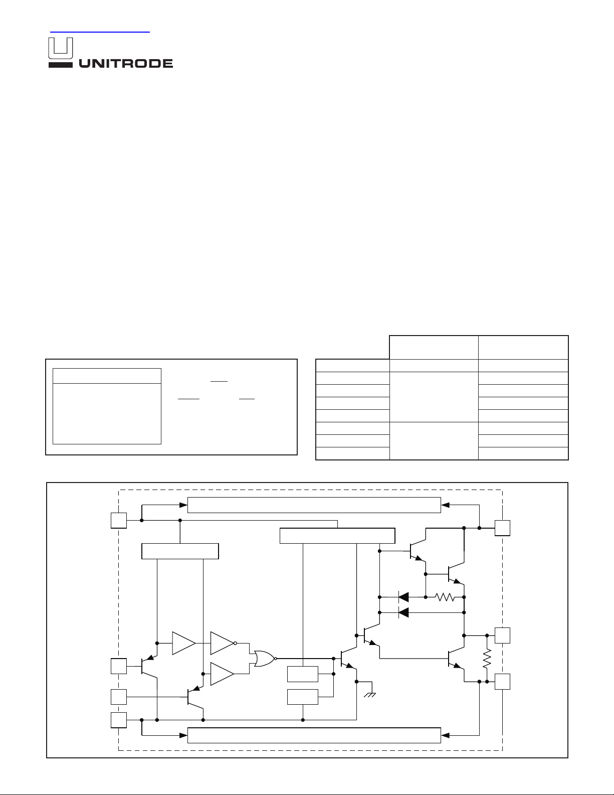
The UC1710 family of FET drivers is made with a high-speed Schottky pro-
cess to interface between low-level control functions and very high-power
switching devices-particularly power MOSFET’s. These devices accept
low-current digital inputs to activate a high-current, totem pole output which
can source or sink a minimum of 6A.
Supply voltages for both V
IN
and V
C
can independently range from 4.7V to
18V. These devices also feature under-voltage lockout with hysteresis.
The UC1710 is packaged in an 8-pin hermetically sealed dual in-line pack-
age for –55°C to +125°C operation. The UC2710 and UC3710 are speci-
fied for a temperature range of –40°C to +85°C and 0°C to +70°C
respectively and are available in either an 8-pin plastic dual in-line or a
5-pin, TO-220 package. Surface mount devices are also available.
INV N.I. Out
HHL
LHH
HLL
LLL
TRUTH TABLE
5
3
7
4
V
C
INTERNALLY CONNECTED IN T PACKAG E
OUTPUT BIAS
V
IN
LOGIC BIAS
Out
2PwrGnd
TSD
UVLO1
8
Logic G nd
INV IN
N.I. IN
INTERNALLY CO NNECTED IN T PACKAGE
BLOCK DIAGRAM
UDG-99079
OUT= INV and N.I.
OUT
= INV or N.I.
TEMPERATURE
RANGE
PACKAGE
UC1710J –55°C to +125°C 8 pin CDIP
UC2710DW –40°C to +85°C 16 pin SOIC-wide
UC2710J 8 pin CDIP
UC2710N 8 pin PDIP
UC2710T 5 pin TO220
UC3710DW 0°C to +70°C 16 pin SOIC-wide
UC3710N 8 pin PDIP
UC3710T 5 pin TO220
ORDERING INFORMATION
查询UC2710供应商
2
UC1710
UC2710
UC3710
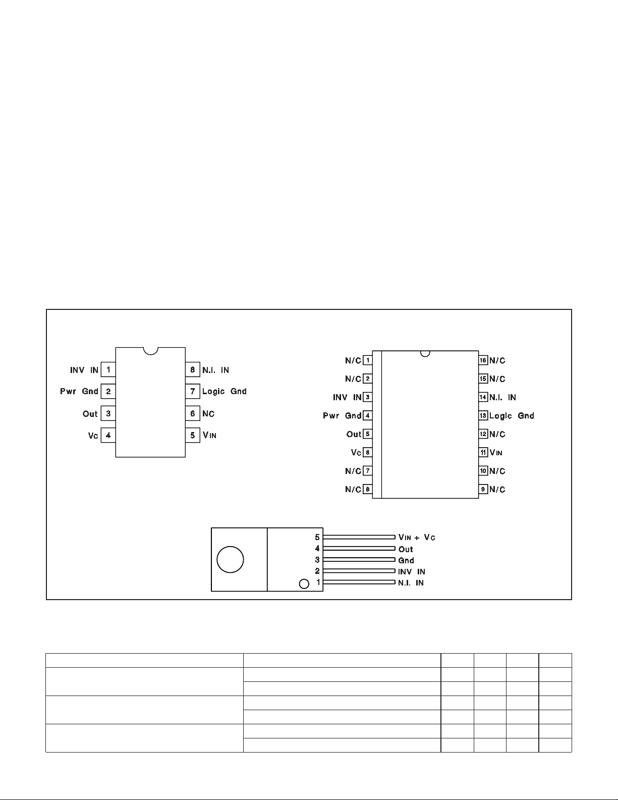
CONNECTION DIAGRAMS
N-Package J-Package T-Package
Supply Voltage, Vin . . . . . . . . . . . . . . . . . . . . . . . . . . . 20V . . . . . . . . . . . . . . 20V . . . . . . . . . . . . . . 20V
Collector Supply Voltage, V
C
. . . . . . . . . . . . . . . . . . . . 20V . . . . . . . . . . . . . . 20V . . . . . . . . . . . . . . 20V
Operating Voltage . . . . . . . . . . . . . . . . . . . . . . . . . . . . 18V . . . . . . . . . . . . . . 18V . . . . . . . . . . . . . . 18V
Output Current (Source or Sink)
Steady-State. . . . . . . . . . . . . . . . . . . . . . . . . . . . . ± 500mA. . . . . . . . . . . .
±
500mA . . . . . . . . . . . . . ± 1A
Digital Inputs. . . . . . . . . . . . . . . . . . . . . . . . . . . . –0.3V-VIN . . . . . . . . –0.3V – V
IN
. . . . . . . . –0.3V – VIN
Power Dissipation at Ta=25°C . . . . . . . . . . . . . . . . . . . 1W. . . . . . . . . . . . . . . 1W. . . . . . . . . . . . . . . 3W
Power Dissipation at T (Case) = 25°C. . . . . . . . . . . . . . 2W . . . . . . . . . . . . . . . 2W . . . . . . . . . . . . . . 25W
Operating Junction Temperature. . . . . . . –55°C to +150°C . . . . –55°C to +150°C . . . . –55°C to +150°C
Storage Temperature . . . . . . . . . . . . . . . –65°C to +150°C . . . . –65°C to +150°C . . . . –65°C to +150°C
Lead Temperature (Soldering, 10 seconds). . . . . . . 300°C . . . . . . . . . . . . 300°C . . . . . . . . . . . . 300°C
Note 1: All currents are positive into, negative out of the specified terminal.
Note 2: Consult Unitrode Integrated Circuits databook for information regarding thermal specifications
and limitations of packages.
ABSOLUTE MAXIMUM RATINGS
DIL-8 MINIDIP (Top View)
J or N Package
SOIC-16 (Top View)
DW Package
5-Pin TO-220 (Top View)
T Package
ELECTRICAL CHARACTERISTICS: Unless otherwise stated, these specifications apply for V
IN
= V
C
= 15V, No load,
T
A
= T
J.
PARAMETERS TEST CONDITIONS MIN TYP MAX UNITS
V
IN
Supply Current V
IN
=18V, V
C
=18V, Output Low 26 35 mA
V
IN
=18V, V
C
=18V, Output High 21 30 mA
V
C
Supply Current V
IN
=18V, V
C
=18V, Output Low 1.5 5.0 mA
V
IN
=18V, V
C
=18V,Output High 5.0 8 mA
UVLO Threshold V
IN
High to Low 3.8 4.1 4.4 V
V
IN
Low to High 4.1 4.4 4.8 V
 Loading...