


UNITRODE UCC1807-1, UCC1807-2, UCC1807-3, UCC2807-1, UCC2807-2 Technical data
...
UCC1807
application
INFO
available
UCC1807-1/-2/-3 UCC2807-1/-2/-3 UCC3807-1/-2/-3
Programmable Maximum Duty Cycle PWM Controller
FEATURES
User Programmable Maximum PWM
Duty Cycle
100 A Startup Current
Operation to 1MHz
Internal Full Cycle Soft Start
Internal Leading Edge Blanking of
Current Sense Signal
DESCRIPTION
The UCC3807 family of high speed, low power integrated circuits contains all of the control and drive circuitry required for off-line and DC-to-DC fixed frequency current mode switching power supplies with minimal external parts count.
These devices are similar to the UCC3800 family, but with the added feature of a user programmable maximum duty cycle. Oscillator frequency and maximum duty cycle are programmed with two resistors and a capacitor. The UCC3807 family also features internal full cycle soft start and internal leading edge blanking of the current sense input.
1A Totem Pole Output
BLOCK DIAGRAM
The UCC3807 family offers a variety of package options, temperature range options, and choice of critical voltage levels. The family has UVLO thresholds and hysteresis levels for off-line and battery powered systems. Thresholds are shown in the table below.
Part Number |
Turn-on Threshold |
Turn-off Threshold |
Packages |
UCCx807-1 |
7.2V |
6.9V |
J |
UCCx807-2 |
12.5V |
8.3V |
N, D |
UCCx807-3 |
4.3V |
4.1V |
N, D, PW |
|
UDG-95001-1 |
SLUS163 - JUNE 1997 |
1 |
UCC1807-1/-2/-3
UCC2807-1/-2/-3
UCC3807-1/-2/-3
ABSOLUTE MAXIMUM RATINGS |
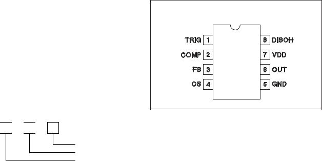
CONNECTION DIAGRAMS |
Supply Voltage (IDD 10mA). . . . . . . . . . . . . . . . . . . . . . . 13.5V Supply Current . . . . . . . . . . . . . . . . . . . . . . . . . . . . . . . . . 30mA
OUT Current . . . . . . . . . . . . . . . . . . . . . . . . . . . . . . . . . . . . ±1A Analog Inputs (FB, CS) . . . . . . . . . . . . . –0.3V to (VDD + 0.3V) Power Dissipation at TA +25°C (N or J packages) . . . . . . . . 1W Power Dissipation at TA +25°C (D package) . . . . . . . . . . 0.65W Storage Temperature . . . . . . . . . . . . . . . . . . . –65°C to +150°C Junction Temperature. . . . . . . . . . . . . . . . . . . –65°C to +150°C Lead Temperature (Soldering, 10 sec.) . . . . . . . . . . . . . +300°C
All currents are positive into, negative out of the specified terminal. Consult Packaging Section of Databook for thermal limitations and considerations of packages.
ORDERING INFORMATION
UCC 
 807
807 
 –
–
UVLO Threshold
Package
Temperature Range
DIL-8, SOIC-8, TSSOP-8 (Top View) J, N, D or PW Packages
ELECTRICAL CHARACTERISTICS:Unless otherwise stated these specifications apply for TA = –55°C to +125°C for
UCC1807-1/-2/-3; –40°C to +85°C for UCC2807-1/-2/-3; and 0°C to +70°C for UCC3807-1/-2/-3; VDD = 10V (Note 6), R = 12k ,
A
RB = 4.7k , CT = 330pF, 1.0 F capacitor from VDD to GND, TA = TJ.
PARAMETER |
TEST CONDITIONS |
MIN |
TYP |
MAX |
UNITS |
Oscillator Section Section |
|
|
|
|
|
Frequency |
|
175 |
202 |
228 |
kHz |
Temperature Stability |
(Note 5) |
|
2.5 |
|
% |
Amplitude |
(Note 1) |
|
1/3VDD |
|
V |
Error Amplifier Section |
|
|
|
|
|
Input Voltage |
COMP = 2.0V |
1.95 |
2.00 |
2.05 |
V |
Input Bias Current |
|
–1 |
|
1 |
A |
Open Loop Voltage Gain |
|
60 |
80 |
|
dB |
COMP Sink Current |
FB = 2.2V, COMP = 1.0V |
0.3 |
2.5 |
|
mA |
COMP Source Current |
FB = 1.3V, COMP = 4.0V |
–0.2 |
–0.5 |
|
mA |
PWM Section |
|
|
|
|
|
Maximum Duty Cycle |
|
75 |
78 |
81 |
% |
Minimum Duty Cycle |
COMP = 0V |
|
|
0 |
% |
Current Sense Section |
|
|
|
|
|
Gain |
(Note 2) |
1.1 |
1.65 |
1.8 |
V/V |
Maximum Input Signal |
COMP = 5.0V (Note 3) |
0.9 |
1.0 |
1.1 |
V |
Input Bias Current |
|
–200 |
|
200 |
nA |
CS Blank Time |
|
50 |
100 |
150 |
ns |
Overcurrent Threshold |
|
1.4 |
1.5 |
1.6 |
V |
COMP to CS Offset |
CS = 0V |
0.55 |
1.1 |
1.65 |
V |
Output Section |
|
|
|
|
|
OUT Low Level |
I = 100mA |
|
0.4 |
1 |
V |
OUT High Level |
I = –100mA, VDD - OUT |
|
0.4 |
1 |
V |
Rise/Fall Time |
CL = 1nF (Note 5) |
|
20 |
100 |
ns |
Undervoltage Lockout Section |
|
|
|
|
|
2

UCC1807-1/-2/-3
UCC2807-1/-2/-3
UCC3807-1/-2/-3 ELECTRICAL CHARACTERISTICS:Unless otherwise stated these specifications apply for TA = –55°C to +125°C for
UCC1807-1/-2/-3; –40°C to +85°C for UCC2807-1/-2/-3; and 0°C to +70°C for UCC3807-1/-2/-3; VDD = 10V (Note 6), R = 12k ,
A
RB = 4.7k , CT = 330pF, 1.0 F capacitor from VDD to GND, TA = TJ.
PARAMETER |
|
TEST CONDITIONS |
MIN |
TYP |
MAX |
UNITS |
||
Start Threshold |
|
UCCx807-1 (Note 4) |
6.6 |
7.2 |
7.8 |
V |
||
|
|
|
|
UCCx807-2 |
11.5 |
12.5 |
13.5 |
V |
|
|
|
|
UCCx807-3 |
4.1 |
4.3 |
4.5 |
V |
Minimum Operating Voltage After Start |
|
UCCx807-1 (Note 4) |
6.3 |
6.9 |
7.5 |
V |
||
|
|
|
|
UCCx807-2 |
7.6 |
8.3 |
9.0 |
V |
|
|
|
|
UCCx807-3 |
3.9 |
4.1 |
4.3 |
V |
Hysteresis |
|
UCCx807-1 |
0.1 |
0.3 |
0.5 |
V |
||
|
|
|
|
UCCx807-2 |
3.5 |
4.2 |
5.1 |
V |
|
|
|
|
UCCx807-3 |
0.1 |
0.2 |
0.3 |
V |
Soft Start Section |
|
|
|
|
|
|
||
COMP Rise Time |
|
FB = 1.8V, From 0.5V to 4.0V |
|
4 |
|
ms |
||
Overall Section |
|
|
|
|
|
|
||
Startup Current |
|
VDD < Start Threshold (UCCx807-1,-3) |
|
0.1 |
0.2 |
mA |
||
|
|
|
|
VDD < Start Threshold (UCCx807-2) |
|
0.15 |
0.25 |
mA |
Operating Supply Current |
|
FB = 0V, CS = 0V, No Load (Note 7) |
|
1.3 |
2.1 |
mA |
||
VDD Zener Shunt Voltage |
|
IDD = 10mA |
12.0 |
13.5 |
15.0 |
V |
||
Shunt to Start Difference |
|
|
0.5 |
1.0 |
|
V |
||
Note 1: Measured at TRIG; signal minimum = 1/3 VDD, maximum = 2/3 VDD. |
|
|
|
|
||||
Note 2: Gain is defined by: A |
VCOMP |
, 0 |
VCS 0.8V |
|
|
|
|
|
|
|
|
|
|
||||
|
VCS |
|
|
|
|
|
|
|
Note 3: Parameter measured at trip point of latch with FB at 0V.
Note 4: Start Threshold and Zener Shunt thresholds track one another.
Note 5: Ensured by design. Not 100% tested in production.
Note 6: Adjust VDD above the start threshold before setting at 10V for UCC3807-2.
Note 7: Does not include current in external timing RC network.
PIN DESCRIPTIONS
COMP: COMP is the output of the error amplifier and the input of the PWM comparator. The error amplifier in the UCC3807 is a low output impedance, 2MHz operational amplifier. COMP can both source and sink current. The error amplifier is internally current limited, which allows zero duty cycle by externally forcing COMP to GND.
The UCC3807 family features built-in full cycle soft start. Soft start is implemented as a clamp on the maximum COMP voltage.
CS: Current sense input. There are two current sense comparators on the chip, the PWM comparator and an overcurrent comparator.
The UCC3807 also contains a leading edge blanking circuit, which disconnects the external CS signal from the current sense comparator during the 100ns interval immediately following the rising edge of the signal at the OUT pin. In most applications, no analog filtering is required on CS. Compared to an external RC filtering technique, leading edge blanking provides a smaller effective CS to OUT propagation delay. Note, however, that the minimum non-zero on-time of the OUT signal is directly
affected by the leading edge blanking and the CS to OUT propagation delay.
The overcurrent comparator is only intended for fault sensing. Exceeding the overcurrent threshold causes a soft start cycle.
FB: The inverting input to the error amplifier. For best stability, keep connections to FB as short as possible and stray capacitance as small as possible.
GND: Reference ground and power ground for all functions of the part.
OUT: The output of a high current power driver capable of driving the gate of a power MOSFET with peak currents exceeding 1A. OUT is actively held low when VDD is below the UVLO threshold.
The high current power driver consists of MOSFET output devices in a totem pole configuration. This allows the output to switch from VDD to GND. The output stage also provides a very low impedance which minimizes overshoot and undershoot. In most cases, external Schottky clamp diodes are not required.
3
 Loading...