


查询UCC1806供应商
application
INFO
available
Low Power, Dual Output, Current Mode PWM Controller
FEATURES
BiCMOS Version of UC1846 Families
•
1.4mA Maximum Operating Current
•
100µA Maximum Startup Current
•
1.0A Peak Output Current
•
125nsec Circuit Delay
•
Easier Parallelability
•
Improved Benefits of Current Mode
•
Control
DESCRIPTION
The UCC1806 family of BiCMOS PWM controllers offers exceptionally im
proved performance with a familiar architecture. With the same block dia
gram and pinout of the popular UC1846 series, the UCC1806 line features
increased switching frequency capability while greatly reducing the bias
current used within the device. With a typical startup current of 50µA and a
well defined voltage threshold for turn-on, these devices are favored for ap
plications ranging from off-line power supplies to battery operated portable
equipment. Dual high current, FET driving outputs and a fast current sense
loop further enhance device versatility.
All the benefits of current mode control including simpler loop closing, volt
age feed-forward, parallelability with current sharing, pulse-by-pulse current
limiting, and push-pull symmetry correction are readily achievable with the
UCC1806 series.
UCC1806
UCC2806
UCC3806
-
-
-
-
(continued)
BLOCK DIAGRAM
10
SYNC
4.4V 1.5V
9RT
8
CT
CS–
CS+
INV
COMP
VIN
3
4
NI
5
6
7
15
LO
3X
–
+
EA
7.0V
7.5V
15V
OSC
0.5V
5.1V
REFERENCE
REGULATOR
S
R
4.25V
COMP
120µA
Q
R
S
1
S
2
S
1
S
2
R
REFERENCE LOW
QB
Q
T
SHUTDOWN
LOCK OUT
UNDER VOLTAGE LOCKOUT
Q
QB
200µA
R
Q
S
CURRENT LIMIT
RESTART
0.35V
1.00V
13 VC
11 AOUT
14 BOUT
12 GND
16
200k
1
CURLIM
SHUTDOWN
2
VREF
Pin numbers refer to DIL-16 package.
SLUS272A - FEBRUARY 2000
UDG-99035

ABSOLUTE MAXIMUM RATINGS
Supply Voltage, Low Impedance (Pin 15) . . . . . . . . . . . . . +15V
Supply Current, High Impedance (Pin 15) . . . . . . . . . . . +25mA
Output Supply Voltage (Pin 13). . . . . . . . . . . . . . . . . . . . . +18V
Output Current, Continuous Source or Sink. . . . . . . . . ±200mA
Output Current, Gate Drive. . . . . . . . . . . . . . . . . . . . . .±500mA
Analog Input Voltage (Pin 3, 4, 5, 6, 16) . . −0.3V to +V
Sync Output Current (Pin 10) . . . . . . . . . . . . . . . . . . . . .±30mA
Error Amplifier Output Current (Pin 7) . +10mA/− (Self Limiting)
Power Dissipation at T
Power Dissipation at T
Storage Temperature Range . . . . . . . . . . . . . . 65°C to +150°C
Lead Temperature (soldering, 10 seconds). . . . . . . . . . +300°C
= 25°C (Note 3). . . . . . . . . . . 1000mW
A
= 25°C (Note 3). . . . . . . . . . . 2000mW
C
IN +0.3V
Note 1. All voltages are with respect to Ground, Pin 12.
Note 2. Currents are positive into, negative out of the specified
terminal.
Note 3. Consult packaging section of databook for thermal limi
tations and considerations of package.
Note 4. Pin numbers refer to DIL-16 package.
CONNECTION DIAGRAMS
DESCRIPTION (continued)
These devices are available with multiple package op
tions for both through-hole and surface mount applica
tions; and in commercial, industrial, and military
temperature ranges.Contact factory for availability.
The UCC1806 is specified for operation from –55°C to
+125°C, the UCC2806 is specified for operation from
–40°C to +85°C, and the UCC3806 is specified for oper
ation from 0°C to +70°C.The part is available in DIP and
SOIC packages.
-
UCC1806
UCC2806
UCC3806
-
-
-
DIL-16 (Top View)
J or N, DW PACKAGE
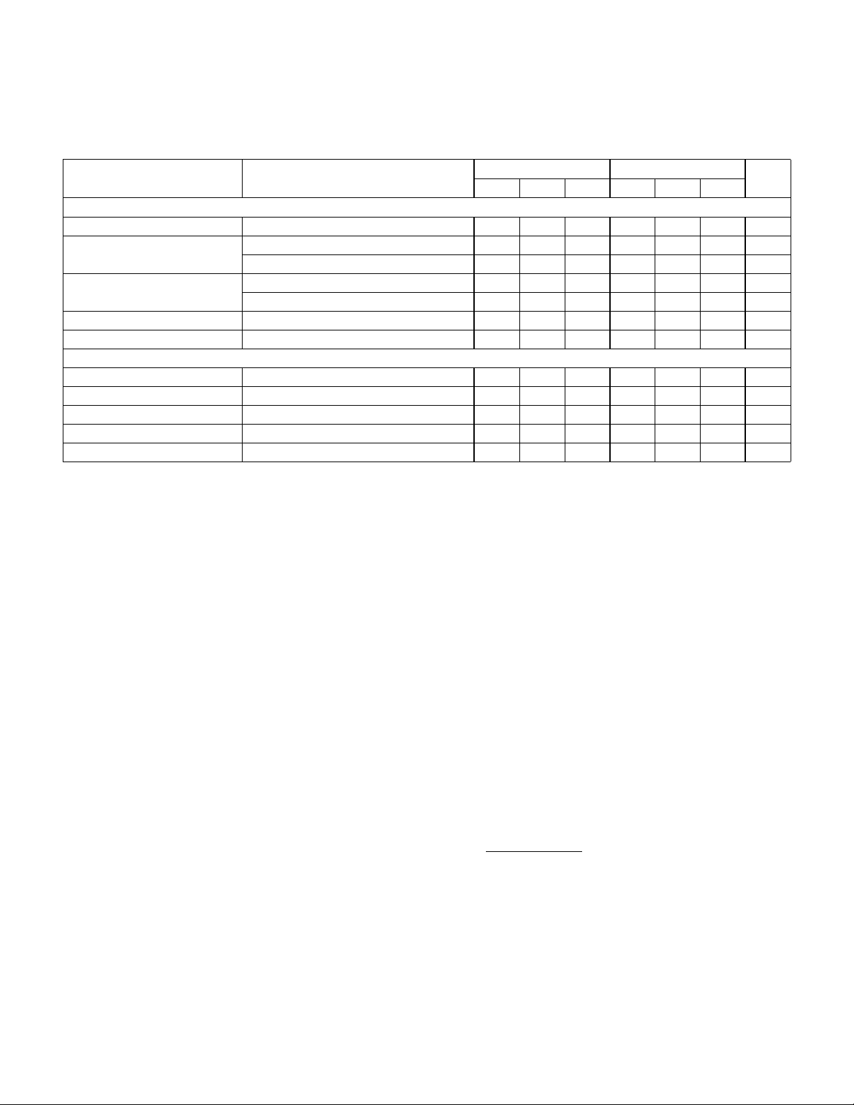
ELECTRICAL CHARACTERISTICS: Unless otherwise stated, these specifications hold for TA= –55°C to +125°C for the
UCC1806, −40°C to +85°C for the UCC2806, and 0°C to +70°C for the UCC3806; V
C
BYPASS
Reference Section
on V
PARAMETER TEST CONDITION UCC1806 / UCC2806 UCC3806 UNITS
Output Voltage T
Load Regulation 0.2mA < I
Total Output Variation Line, Load, Temperature (Note 7) −150 150 −150 150 mV
Output Noise Voltage 10Hz ≤ f ≤ 10kHz, T
Long Term Stability T
Output Short Circuit −10 −30 −10 −30 mA
= 0.01µF, TA=TJ.
REF
= 25°C, IO= 0.2mA 5.02 5.10 5.17 5.00 5.10 5.20 V
J
< 5mA 3 25 3 25 mV
O
= 25°C
(Note 5)
= 125°C, 1000 Hours (Note 5) 5 25 5 25 mV
A
J
PLCC-20, LCC-20 (Top View)
Q, L PACKAGE
= 12V, RT= 33k, CT = 330pF,
IN
MIN TYP MAX MIN TYP MAX
70 70 µV
2

UCC1806
UCC2806
UCC3806
ELECTRICAL CHARACTERISTICS: Unless otherwise stated, these specifications hold for TA= –55°C to +125°C for the
UCC1806, −40°C to +85°C for the UCC2806, and 0°C to +70°C for the UCC3806; V
C
BYPASS
on V
= 0.01µF, TA=TJ.
REF
PARAMETER TEST CONDITION UCC1806 / UCC2806 UCC3806 UNITS
MIN TYP MAX MIN TYP MAX
Oscillator Section
Initial Accuracy T
Temperature Stability T
= 25°C 424752424752kHz
J
MIN
< TA<T
(Note 5) 2 2 %
MAX
Amplitude 2.35 2.35 V
SYNC Delay to Outputs Pin 8 = 0V, Pin 9 = V
V
= 0.8V to 2.0V
SYNC
Discharge Current T
SYNC, V
SYNC, V
SYNC, V
SYNC, V
OL
OH
IL
IH
= 25°C, V
J
I
= +1mA 0.4 0.4 V
OUT
I
= –4mA 2.4 2.4 V
OUT
8 = 2.0V 2 2 mA
PIN
Pin 8 = 0V, Pin 9 = V
Pin 8 = 0V, Pin 9 = V
REF
REF
REF
,
2.0 2.0 V
SYNC Input Current −1+1−1+1µA
Error Amplifier Section
Input Offset Voltage 5 10 mV
Input Bias Current −1 −1 µA
Input Offset Current 500 500 nA
Common Mode Range 0 V
Open Loop Gain V
= 1.0 to 4.0 80 100 80 100 dB
O
Unity Gain Bandwidth 1 1 MHz
Output Sink Current V
Output Source Current V
Output High Level V
Output Low Level V
< –20mV, V
ID
< 20mV, V
ID
= –50mV 4.5 4.5 V
ID
= –50mV 0.5 0.5 V
ID
= 1.0V 1 1 mA
PIN 7
= 3.0V −80 −120 −80 −120 µA
PIN 7
Current Sense Amplifier Section
Amplifier Gain V
Maximum Differential Input
Signal (V
PIN 4 -VPIN 3)
Input Offset Voltage V
CMRR V
= 0V, V
PIN 3
V
PIN 1=VREF,VPIN 5=VREF
V
= 0V
PIN 6
= 0.5V, V
PIN 1
= 0 to VIN– 3.5 60 60 dB
CM
PIN 1=VREF
PIN 7
(Notes 3,4) 2.75 3 3.35 2.75 3 3.35 V/V
,
1.1 1.1 V
= OPEN 10 30 10 50 mV
PSRR 56 56 dB
Input Bias Current V
Input Offset Current V
Delay to Outputs V
= 0.5V, PIN 7 OPEN (Note 3) −1 −1 µA
PIN 1
PIN 1 = 0.5V, PIN 7 OPEN (Note 3) 1 1 µA
PIN 5=VREF
, PIN 6 = 0, PIN 1 = 2.75V,
PIN 4 – PIN 3 = 0 to 1.5V step (Note 6)
Current Limit Adjust Section
Current Limit Offset V
PIN 3
= 0, V
= 0, PIN 7 = open 0.40 0.50 0.60 0.40 0.50 0.60 V
PIN 4
Input Bias Current 11µA
Minimum Latching Current 300 200 300 200 µA
Maximum Non-Latching
Current
Shutdown Terminal Section
Threshold Voltage 0.94 1.00 1.06 0.9 1.0 1.1 V
Input Voltage Range 0 V
Delay to Outputs V
= 0 to 1.3V 75 150 75 150 ns
PIN 16
= 12V, RT= 33k, CT = 330pF,
IN
50 125 50 100 ns
0.8 0.8 V
-2 0 VIN−2V
IN
125 175 125 175 ns
200 80 200 80 µA
IN 0VIN V
3
UCC1806
UCC2806
UCC3806
ELECTRICAL CHARACTERISTICS: Unless otherwise stated, these specifications hold for TA= –55°C to +125°C for the
UCC1806, −40°C to +85°C for the UCC2806, and 0°C to +70°C for the UCC3806; V
C
BYPASS
Output Section
Under Voltage Lockout Section
on V
PARAMETER TEST CONDITION UCC1806 / UCC2806 UCC3806 UNITS
Output Supply Voltage 2.5 15 2.5 15 V
Output Low Level I
Output High Level I
Rise Time T
Fall Time T
Startup Current V
Operating Supply Current 1 1.4 1 1.4 mA
V
IN Shunt Voltage I
Startup Threshold 6.5 7.5 8 6.5 7.5 8 V
Threshold Hysteresis 0.75 0.75 V
= 0.01µF, TA=TJ.
REF
MIN TYP MAX MIN TYP MAX
= 20mA 100 300 100 200 mV
SINK
I
= 100mA 0.40 1.1 0.40 1.1 V
SINK
SOURCE
I
SOURCE
VIN
= −20mA 11.6 11.9 11.6 11.9 V
= −100mA 11 11.6 11 11.6 V
= 25°C, C
J
= 25°C, C
J
< Start Threshold 50 100 50 100 µA
IN
= 10mA 15 17.5 15 17.5 V
= 1000pF 35 65 35 65 ns
LOAD
= 1000pF 35 65 35 65 ns
LOAD
= 12V, RT= 33k, CT = 330pF,
IN
Note 1: All voltages are with respect to Ground, Pin 12.
Note 2: Currents are positive into, negative out of the specified terminal.
Note 3: Parameters measured at trip point of latch with V
Note 4: Amplifier gain defined as: G = delta change at Pin 7/delta change forced at Pin 4 delta voltage at Pin 4 = 0 to 1V.
Note 5: Guaranteed by design. Not 100% tested in production.
Note 6: Current Sense Amp output is slew rate limited to provide noise immunity.
Note 7: Line Range = 10V to 15V, Load Range = 0.2mA to 5mA.
PIN 5=VREF,VPIN 6
= 0V.
PIN DESCRIPTIONS
AOUT and BOUT: AOUT and BOUT provide alternating
high current gate drive for the external MOSFETs. Duty
cycle can be varied from 0 to 50% where minimum dead
time is a function of CT. Both outputs use MOS transistor
switches with inherent anti-parallel body diodes to clamp
voltage swings to the supply rails, allowing operation
without the use of clamp diodes.
COMP: COMP is the output of the error amplifier and the
input of the PWM comparator.The error amplifier is a low
output impedance, 2MHz operational amplifier which al
lows sinking or sourcing of current at the COMP pin. The
error amplifier is internally current limited, so that zero
duty cycle can be commanded by externally forcing
COMP to GND.
CS–: CS- is the inverting input of the 3X, differential cur
rent sense amplifier.
CS+: CS+ is the non-inverting input of the 3X, differential
current sense amplifier.
CT: CT is the oscillator timing capacitor connection point,
which is charged by the current set by RT. CT is dis
charged to GND through a 2.6mA current sink. This
causes a linear discharge of CT to zero volts which then
initiates the next switching cycle. Dead time occurs dur
ing the discharge of CT, forcing AOUT and BOUT low.
Switching frequency (fs) and dead time (td) are approxi
mated by:
fs
=
-
2
1
RT CT td
••+
andtd CT
=•
961
CURLIM: CURLIM programs the primary current limit
threshold and determines whether the device will latch
off or retry after an overcurrent condition. When a shut
down signal is generated, a 200µA current source to
-
ground pulls down on CURLIM. If the voltage on the pin
remains above 350mV the device remains latched and
the power must be cycled to restart. If the voltage on the
pin falls below 350mV, the device attempts a restart. The
voltage threshold is typically set by a resistor divider from
-
-
-
-
4
PIN DESCRIPTIONS (continued)
V
to ground. To calculate the current limit adjust volt
REF
age threshold the following equations can be used;
Current Limit Adjust Latching Mode Voltage:
VR A
REF
V
=
Current Limit Adjust Non-Latching Mode Voltage:
VRA
REF
V
=
where R1 is the resistance from the V
and R2 is the resistance from CURLIM to GND.
GND: GND is the reference ground and power ground for
all functions of this part. Bypass and timing capacitors
should be connected as close as possible to GND.
INV: INV is the inverting input of the error amplifier and
has a common mode range from 0V to V
NI: NI is the non-inverting input of the error amplifier and
has a common mode range from 0V to V
RT: RT is the connection point for the oscillator timing resistor. It has a low impedance input and is nominally at
1.25V. The current through RT is mirrored to the timing
capacitor pin, CT. This causes a linear charging of CT
from 0V to 2.35V.Note that the current mirror is limited to
a maximum of 100µA so RT must be greater than 12.5k.
•
–( )1 300
R
1
+
1
R
2
•
–( )180
R
1
+
1
R
2
µ
mV
>
350
µ
mV
>
350
to CURLIM
REF
–2V.
IN
–2V.
IN
UCC1806
UCC2806
UCC3806
-
SHUTDOWN: The SHUTDOWN pin is provided for en
hanced protection. When SHUTDOWN is driven above
1V, AOUT and BOUT are forced low.
SYNC: SYNC is a bi-directional pin, allowing or providing
external synchronization with TTL compatible thresholds.
In a typical application RT is connected through a timing
resistor to GND which allows the internal oscillator to
free run. In this mode SYNC outputs a TTL compatible
pulse during the oscillator dead time (when CT is being
discharged). If RT is forced above 4.4V, SYNC acts as an
input with TTL compatible thresholds and the internal os
cillator is disabled. When SYNC is high, greater than 2V
the outputs are held active low.When SYNC returns low,
the outputs may be high until the on-time is terminated
by the normal peak current signal, a fault seen at SHUT
DOWN or the next high assertion of SYNC. Multiple
UCC3806s can be synchronized by a single master
UCC3806 or external clock.
VC: VC is the input supply connection for the FET drive
outputs and has an input range of 2.5V to 15V. VC
should be capacitively bypassed for proper operation.
: VINis the input supply connection for this device.
V
IN
The UCC1806 has a maximum startup threshold of 8V
and internally limited by means of a 15V shunt regulator.
The shunted supply current must be limited to 2.5mA.
For proper operation, VIN must be bypassed to GND with
at least a 0.01µF ceramic capacitor.
: V
V
REF
a 5mA maximum available current. V
passed to GND with at least a 0.1µF ceramic capacitor
for proper operation.
is a 5.1V ±1% trimmed reference output with
REF
must be by
REF
-
-
-
-
TYPICAL CHARACTERISTICS
80
60
40
ain (dB)
G
20
0
-20
1k
10k 100k 1M
Frequency (Hz)
Figure 1. Error amplifier gain and phase response.
135
90
45
0
10M
60
58
56
54
°)
Phase (
52
50
48
46
Oscillator Frequency (kHz)
44
42
40
-55-50 -25 0 25 50 75 100 125
Temperature (°C)
Figure 2. Oscillator frequency vs.temperature.
5
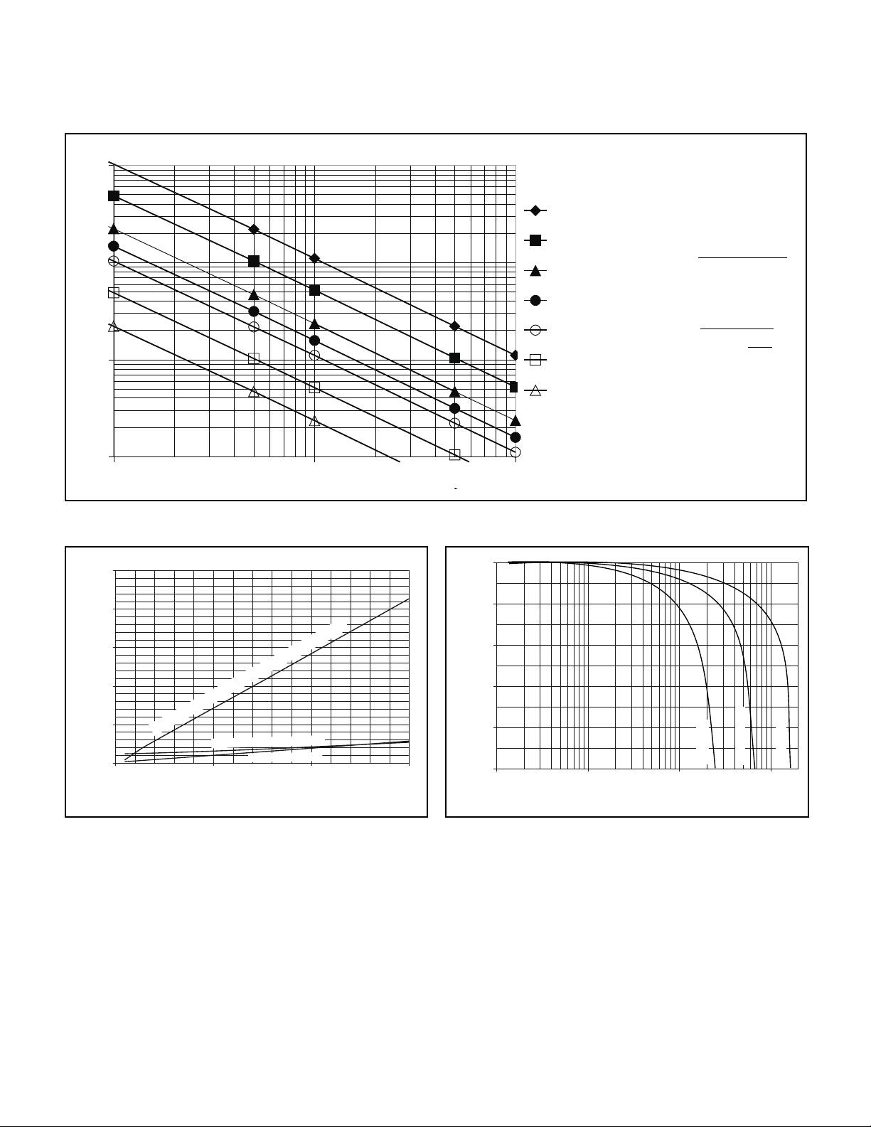
TYPICAL CHARACTERISTICS (continued)
UCC1806
UCC2806
UCC3806
1M
100k
10k
1
10k 100k 1M
Figure 3. Oscillator frequency vs.RT and CT.
25
50
CT=
47pF
100pF
220pF
330pF
470pf
1.0nF
2.2nF
Design Equations
for Oscillator:
F
=
OSC
TRTCT
T
RAMP
FALL
=••19 2.
=
DeadTime T
1
TT
+
RAMP FALL
CT
•24
.
125
0002
. –
.
RT
=
FALL
20
15
Ω
10
Supply Current (mA)
5
0
0
C
I @ Output Load = 1nF, 10 Series Resistance
Load or No Load
IN
I@
500k 1M 1.5M
Oscillator Frequency (Hz)
C
I@
No Load
Figure 4. Supply current vs.oscillator frequency.
45
40
35
30
Maximum Duty Cycle (%)
T
25
1k
10k
Oscillator Frequency (Hz)
100k 1M
C=1nF
Figure 5. Maximum duty cycle vs. frequency.
T
C=330pF
T
C =100pF
6
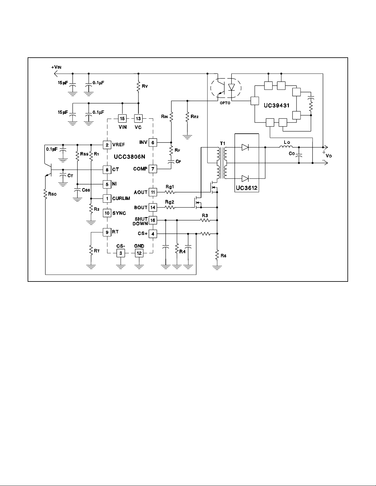
TYPICAL APPLICATION
UCC1806
UCC2806
UCC3806
UNITRODE CORPORATION
7 CONTINENTAL BLVD. • MERRIMACK, NH 03054
TEL. (603) 424-2410 • FAX (603) 424-3460
UDG-95036
7
 Loading...