


UNITRODE UCC18500, UCC18501, UCC18502, UCC18503, UCC28500 Technical data
...
UCC18500
UCC18500/1/2/3
UCC28500/1/2/3
UCC38500/1/2/3
BiCMOS PFC/PWM Combination Controller
PRELIMINARY
FEATURES
•Combines PFC and 2nd Stage Down Converter Function
•Controls Boost PWM to Near-unity Power Factor
•Accurate Power Limiting
•Average Current Mode Control in PFC Stage
•Peak Current Mode Control in Second Stage
•Programmable Oscillator
•Leading Edge/Trailing Edge Modulation for Reduced Output Ripple Using SmartSync™
•Low Startup Supply Current
•Synchronized Second Stage Start-up, with Programmable Soft-start
•Programmable Second Stage Shut-down
DESCRIPTION
The UCC18500 family provides all of the functions necessary for an active power factor corrected preregulator and a second stage DC-to-DC converter. The controller achieves near-unity power factor by shaping the AC input line current waveform to correspond to the AC input line voltage using average current mode control. The DC-to-DC converter uses peak current mode control to perform the step down power conversion.
The PFC stage is leading edge modulated while the second stage is trailing edge synchronized to allow for minimum overlap between the boost and PWM switches. This reduces ripple current in the bulk output capacitor.
In order to operate with a three to one range of input line voltages, a line feedforward (VFF) in used to keep input power constant with varying input voltage. Generation of VFF is done using IAC in conjunction with an external single pole filter. This not only reduces external parts count, but avoids the use of high voltage components offering a lower cost solution. The multiplier then divides the line current by the square of VFF.
(continued)
BLOCK DIAGRAM
|
|
|
|
|
|
|
|
|
VERR |
ISENSE2 |
SS2 |
|
VCC |
GND |
|
|
|
||
|
|
|
|
|
|
|
|
|
7 |
|
|
8 |
13 |
|
9 |
6 |
|
|
|
|
|
|
|
|
|
|
|
|
|
|
|
|
SECOND STAGE |
|
7.5V |
|
20 |
VREF |
|
|
|
|
|
|
|
|
|
|
|
|
|
|
SOFT START |
|
REFERENCE |
|
|||
|
|
|
|
|
|
|
|
|
|
|
|
|
|
|
|
|
|||
|
|
6.75V |
UVLO2 |
|
|
|
|
|
|
|
|
|
|
|
UVLO |
|
|
|
|
OVP/ENBL |
4 |
|
|
|
|
|
|
|
|
|
|
|
|
|
|
VCC |
|
|
|
1.5V |
– |
|
ENABLE |
|
|
|
|
|
|
|
|
16V/10 |
|
|
|||||
|
|
|
|
|
|
|
|
|
|
|
|
||||||||
|
|
|
|
|
|
|
|
|
|
|
|
|
|
|
|||||
|
|
|
|
+ |
|
|
|
|
|
|
|
|
ILIMIT |
|
|
|
|
|
|
|
|
|
|
|
|
|
|
|
|
|
|
1.5V |
1.3V |
R |
|
|
|
10 |
GT2 |
|
|
|
|
8.0V |
+ |
|
PFCOVP |
|
|
|
|
|
|
|
|||||
|
|
|
|
|
|
|
|
|
|
|
|
|
|||||||
|
|
|
|
|
|
|
|
R |
Q |
|
|
|
|
||||||
|
|
|
|
|
|
– |
|
|
|
|
|
|
|
|
|
|
|
||
VAOUT |
1 |
|
|
|
|
|
ZERO |
|
|
|
|
PWM |
S |
|
|
|
|
|
|
|
|
|
|
|
|
|
|
|
|
|
|
|
|
|
|
||||
|
|
VOLTAGE |
|
|
0.25V |
– |
POWER |
|
|
|
|
CLK2 |
|
|
|
|
|
||
|
|
ERROR AMP |
|
|
|
|
|
|
|
|
|
|
|
|
|
|
|
||
|
|
|
|
|
+ |
|
|
|
|
|
|
|
|
|
|
|
|
||
VSENSE |
3 |
– |
|
|
|
|
|
|
|
|
|
|
|
|
|
|
|
|
|
|
X |
|
|
|
|
|
|
|
|
|
|
|
|
VCC |
|
|
|||
|
|
+ |
|
MULT |
|
– |
CURRENT AMP |
– |
|
|
|
|
|
|
|||||
|
|
|
|
X |
|
|
|
+ |
|
|
|
S |
Q |
|
|
|
|
|
|
|
|
7.5V |
|
|
|
|
|
|
|
PWM |
|
|
|
|
|
||||
|
|
|
|
|
|
|
|
|
|
|
+ |
PWM |
|
|
|
|
|
||
|
|
|
)2 |
|
|
|
|
|
|
|
|
|
|
|
12 |
GT1 |
|||
VFF |
19 |
(V |
|
|
|
|
|
|
|
|
OSC |
LATCH |
|
|
|
||||
|
|
FF |
|
|
|
|
|
|
|
|
|
|
R |
R |
|
|
|
|
|
|
|
|
|
|
|
|
|
|
|
|
|
CLK1 |
|
|
|
|
|
||
|
|
|
|
|
|
|
|
|
|
|
|
|
|
|
|
|
|
|
|
|
|
MIRROR |
|
|
|
|
|
|
|
|
|
CLK2 |
|
|
|
|
|
11 |
PWRGND |
|
|
2:1 |
|
|
|
|
|
|
|
|
|
|
|
|
|
|
|
|
|
|
|
|
|
|
|
|
|
|
|
|
|
|
|
|
|
|
|
|
|
|
|
|
|
|
|
|
|
|
CLK2 |
|
|
|
CLK1 |
|
ILIMIT |
|
|
|
|
IAC |
18 |
|
|
|
|
|
|
|
OSCILLATOR |
|
|
|
– |
14 |
PKLMT |
||||
|
|
|
|
|
|
|
|
|
|
|
|
|
|
|
|||||
|
|
|
|
|
|
|
|
|
|
|
|
|
|
|
|
|
|||
MOUT |
17 |
|
|
|
|
|
|
|
|
|
|
|
|
|
|
|
+ |
|
|
|
|
|
|
|
|
|
|
|
|
|
|
|
|
|
|
|
|
||
|
|
|
|
|
|
|
|
16 |
15 |
|
2 |
5 |
|
|
|
|
|
|
|
|
|
|
|
|
|
|
ISENSE1 |
CAOUT |
|
RT |
CT |
|
|
|
|
|
|
|
|
|
|
|
|
|
|
|
|
|
|
|
|
|
|
|
|
|
|
|
UDG-98189 |
SLUS419 - AUGUST 1999 |
|
|
|
|
|
|
|
|
|
|
|
|
|
|
|
|
|||
DESCRIPTION (cont.)
The UCC18500 PFC section incorporates a low offset voltage amplifier with 7.5V reference, a highly linear multiplier capable of a wide current range, a high bandwidth, low offset current amplifier, with a novel noise attenuation configuration, PWM comparator and latch and a high current output driver. Additional PFC features include over-voltage protection, zero power detection to turn-off the output when VAOUT is below 0.25V and peak current and power limiting.
The DC-to-DC section relies on an error signal generated on secondary-side and processes it by performing peak current mode control. The DC-to-DC section also features current limiting, a controlled soft-start, preset oper-
UCC18500/1/2/3
UCC28500/1/2/3
UCC38500/1/2/3
ating range with selectable options, and 50% maximum duty cycle.
The UCC38500 and UCC38502 have a wide PFC-UVLO threshold (16.5V/10V) for bootstrap bias supply operation. The UCC38501 and UCC38503 are designed with a narrow UVLO range (10.5V/10V) more suitable for fixed bias operation. The UCC38500 and UCC38501 have a narrow UVLO threshold for PWM stage (to allow operation down to 75% of nominal bulk voltage), while the UCC38502 and UCC38503 are configured for a much wider operation range for the PWM stage (down to 50% of bulk nominal voltage).
ABSOLUTE MAXIMUM RATINGS
Supply Voltage VCC . . . . . . . . . . . . . . . . . . . . . . . . . . . . . . 18V
Gate Drive Current
Continuous . . . . . . . . . . . . . . . . . . . . . . . . . . . . . . . . . . . 0.2A
50% Duty Cycle . . . . . . . . . . . . . . . . . . . . . . . . . . . . . . . . . 1A
Input Voltage
ISENSE1, ISENSE2 MOUT,VSENSE, OVP, ENBL, . . . . . . . . 11V
PKLMT . . . . . . . . . . . . . . . . . . . . . . . . . . . . . . . . . . . . . . . 5V
Input Current, RSET, IAC, PKLMT, ENA . . . . . . . . . . . . . . 10mA
Maximum Negative Voltage, GT1, GT2,
PKLMT, MOUT . . . . . . . . . . . . . . . . . . . . . . . . . . . . . . –0.5V
Power Dissipation. . . . . . . . . . . . . . . . . . . . . . . . . . . . . . . . . 1W
Currents are positive into, negative out of the specified terminal. Consult Packaging Section of Databook for thermal limitations and considerations of packages. All voltages are referenced to GND.
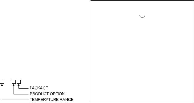
ORDERING INFORMATION
UCC 
 850
850
PACKAGE INFORMATION
CONNECTION DIAGRAMS
DIL-20, SOIC-20 (TOP VIEW)
N, DW and J Packages
VAOUT |
|
|
|
|
|
VREF |
1 |
|
|
|
20 |
||
|
|
|
|
|
|
VFF |
|
|
|
|
|
|
|
RT |
2 |
|
|
|
19 |
|
|
|
|
|
|
|
|
|
|
|
|
|
|
|
VSENSE |
3 |
|
|
|
18 |
IAC |
|
|
|
|
|
|
|
|
|
|
|
|
|
|
OVP/ENA |
4 |
|
|
|
17 |
MOUT |
|
|
|
|
|
|
|
|
|
|
|
|
|
|
CT |
5 |
|
|
|
16 |
ISENSE1 |
|
|
|
|
|
|
|
|
|
|
|
|
|
|
GND |
6 |
|
|
|
15 |
CAOUT |
|
|
|
|
|
|
|
|
|
|
|
|
|
|
VERR |
7 |
|
|
|
14 |
PKLMT |
|
|
|
|
|
|
|
|
|
|
|
|
|
|
ISENSE2 |
8 |
|
|
|
13 |
SS2 |
VCC |
|
|
|
|
|
GT1 |
|
|
|
|
|
||
9 |
|
|
|
12 |
||
|
|
|
|
|
|
|
|
|
|
|
|
|
|
GT2 |
10 |
|
|
|
11 |
PWRGND |
|
|
|
|
|
|
|
|
|
|
|
|
|
|
|
|
|
PRODUCT OPTION |
|
|
|
TEMPERATURE RANGE |
UVLO |
|
UVLO2 HYSTERESIS |
PACKAGE |
UCC18500 |
|
16 |
|
1.2 |
|
UCC18501 |
–55° C to +125° C |
10.5 |
|
1.2 |
J-CDIP |
UCC18502 |
|
16 |
|
3.0 |
N-PDIP |
UCC18503 |
|
10.5 |
|
3.0 |
DW-SOIC |
UCC28500 |
|
16 |
|
1.2 |
|
UCC28501 |
–40° C to +85° C |
10.5 |
|
1.2 |
N-PDIP |
UCC28502 |
|
16 |
|
3.0 |
|
|
|
DW-SOIC |
|||
UCC28503 |
|
10.5 |
|
3.0 |
|
|
|
|
|||
UCC38500 |
|
16 |
|
1.2 |
|
UCC38501 |
0° C to +70° C |
10.5 |
|
1.2 |
|
UCC38502 |
|
16 |
|
3.0 |
|
UCC38503 |
|
10.5 |
|
3.0 |
|
2

UCC18500/1/2/3
UCC28500/1/2/3
UCC38500/1/2/3
ELECTRICAL CHARACTERISTICS: Unless otherwise specified, these specifications hold for TA=0°C to 70°C for the
UCC3850X, –40°C to +85°C for the UCC2850X, and –55°C to +125°C for the UCC1850X, T = T . VCC = 12V, RT = 22k, CT =
A J
330pF.
PARAMETER |
TEST CONDITIONS |
MIN |
TYP |
MAX |
UNITS |
Supply Current Section |
|
|
|
|
|
Supply Current, Off |
VCC = 12V (VCC Turn-on Threshold –300mV) |
|
150 |
300 |
A |
Supply Current, On |
VCC = 12V |
|
4 |
6 |
mA |
UVLO Section |
|
|
|
|
|
VCC Turn-On Threshold (UCCX8500/502) |
|
15.4 |
16 |
16.6 |
V |
UVLO Hysteresis (UCCX8500/502) |
|
5.4 |
6 |
6.2 |
V |
Shunt Voltage (UCCX8500/502) |
IVCC = 10mA |
|
17 |
17.5 |
V |
VCC Turn-On Threshold (UCCX8501/503) |
|
10.2 |
10.5 |
10.8 |
V |
UVLO Hysteresis (UCCX8501/503) |
|
0.4 |
0.5 |
0.6 |
V |
Voltage Amplifier Section |
|
|
|
|
|
Input Voltage |
TA = 0°C to 70°C |
7.388 |
7.500 |
7.613 |
V |
|
TA = –40°C to 85°C |
7.369 |
7.500 |
7.631 |
V |
|
TA = –55°C to125°C |
7.313 |
7.500 |
7.687 |
V |
VSENSE Bias Current |
|
|
50 |
|
nA |
Open Loop Gain |
VAOUT = 2V to 5V |
|
80 |
|
dB |
VOUT High |
ILOAD = –150 A |
5.4 |
5.5 |
5.6 |
V |
VOUT Low |
ILOAD = 150 A |
|
0.05 |
0.10 |
V |
Over Voltage Protection and Enable Section |
|
|
|
|
|
Over Voltage Reference |
|
7.8 |
8.0 |
8.2 |
V |
Hysteresis |
|
400 |
500 |
600 |
mV |
Enable Threshold |
|
1 |
1.5 |
2 |
V |
Current Amplifier Section |
|
|
|
|
|
Input Offset Voltage |
VCM = 0V, VCAOUT = 3V |
–5 |
0 |
5 |
mV |
Input Bias Current |
VCM = 0V, VCAOUT = 3V |
|
–50 |
|
nA |
Input Offset Current |
VCM = 0V, VCAOUT = 3V |
|
25 |
|
nA |
Open Loop Gain |
VCM = 0V, VCAOUT = 2V to 5V |
|
90 |
|
dB |
CMRR |
VCM = 0V to 1.5V, VCAOUT = 3V |
|
80 |
|
dB |
VOUT High |
ILOAD = –120 A |
|
6.3 |
|
V |
VOUT Low |
ILOAD = 1mA |
|
0.2 |
|
V |
Gain Bandwidth Product |
(Note 1) |
|
2.5 |
|
MHz |
Voltage Reference Section |
|
|
|
|
|
Input Voltage |
TA = 0° C to 70° C |
7.388 |
7.500 |
7.613 |
V |
|
TA = –40° C to 85° C |
7.369 |
7.500 |
7.631 |
V |
|
TA = –55° C to 125° C |
7.313 |
7.500 |
7.687 |
V |
Load Regulation |
IREF = 1mA to 2mA |
|
5 |
10 |
mV |
Line Regulation |
VCC = 12V to 16V |
|
10 |
20 |
mV |
Short Circuit Current |
VREF = 0V |
|
–25 |
|
mA |
Oscillator Section |
|
|
|
|
|
Initial Accuracy |
TA = 25°C |
85 |
100 |
115 |
kHz |
Voltage Stability |
VCC = 10.8V to 15V |
|
1 |
|
% |
Total Variation |
Line, Temp |
80 |
|
120 |
kHz |
Ramp Peak Voltage |
|
4.5 |
5 |
5.5 |
V |
Ramp Amplitude Voltage (peak to peak) |
|
|
4 |
|
V |
3
 Loading...