

查询UCC1570供应商
Low Power Pulse Width Modulator
UCC1570
UCC2570
UCC3570
FEATURES
• Low Power BiCMOS Process
• 85µA Start-up Current
• 1mA Run Current
• 1A Peak Gate Drive Output
• Voltage Feed Forward
• Programmable Duty Cycle Clamp
• Optocoupler Interface
• 500kHz Operation
• Soft Start
• Fault Counting Shutdown
• Fault Latch Off or Automatic Restart
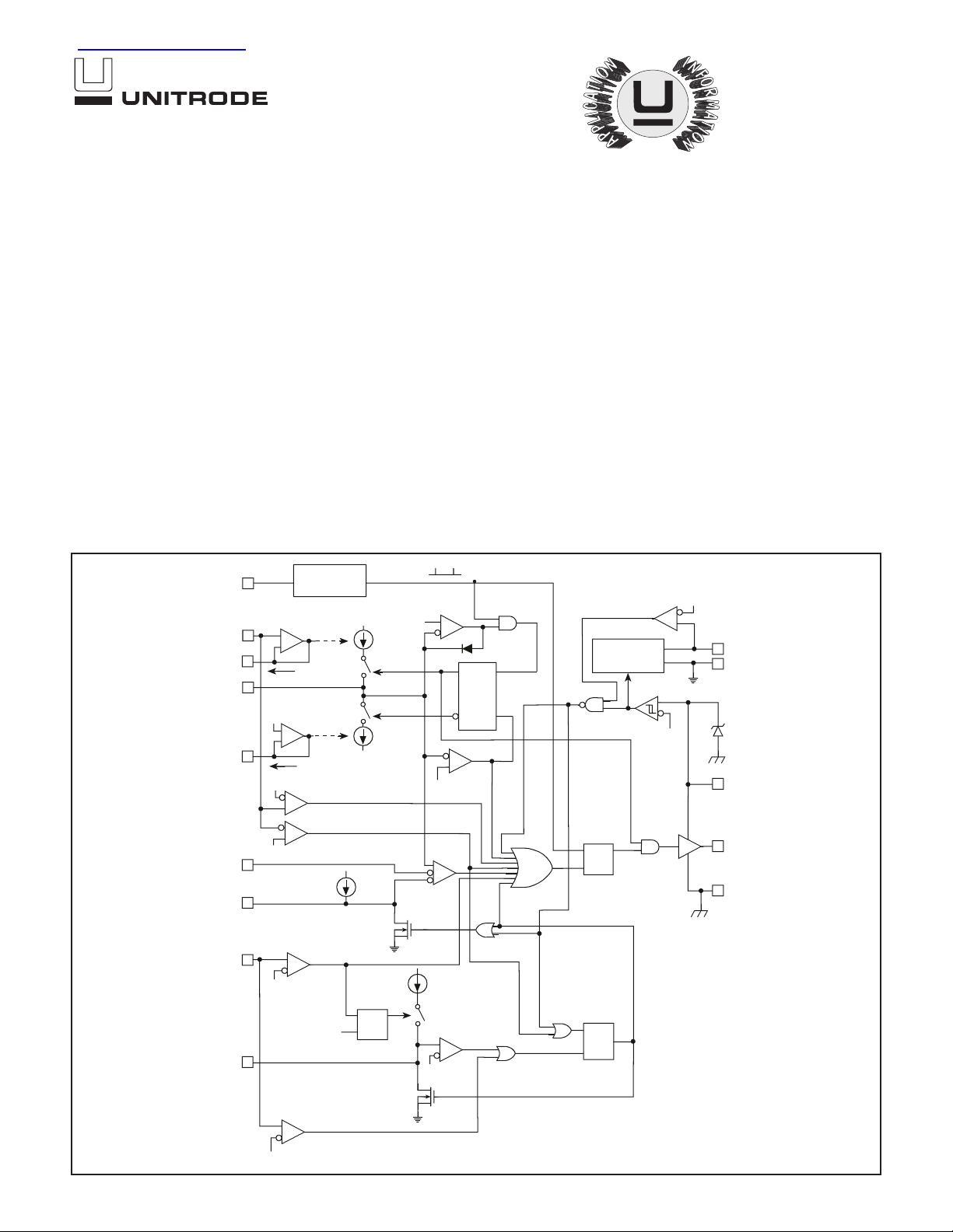
BLOCK DIAGRAM
1V
4V
1V
CLOCK
GENERATOR
I3
I4
HIGH
LINE
LOW
LINE
FREQ
VFWD
SLOPE
RAMP
ISET
FEEDBK
SOFTST
11
6
7
10
9
8
14
DESCRIPTION
The UCC1570 family of pulse width modulators is intended for application
in isolated switching supplies using primary side control and a voltage
mode feedback loop.Made with a BiCMOS process, these devices feature
low startup current for efficient off-line starting with a bootstrapped low voltage supply. Operating current is also very low; yet these devices maintain
the ability to drive a power MOSFET gate at frequencies above 500kHz.
Voltage feedforward provides fast and accurate response to wide line voltage variation without the noise sensitivity of current mode control. Fast current limiting is included with the ability to latch off after a programmable
number of repetitive faults has occurred. This allows the power supply to
ride through a temporary overload, while still shutting down in the event of
a permanent fault. Additional versatility is provided with a maximum duty
cycle clamp programmable within a 20% to 80% range and line voltage
sensing with a programmable window of allowable operation.
CLK
13/9V
4.5V
VREF
12
GND
13
15V
3
VCC
OUT
4
5
PGND
RAMP
VALLEY
1V
10 I3
S
RAMP
LATCH
R
10 I4
RAMP
PEAK
4V
I4
PWM
5V
GENERATOR
S
D
R
PWM
LATCH
04/99
CURLIM
COUNT
CURRENT
0.2V
LIMIT
CLK
SHUTDOWN
I4
SD
R
4V
R
D
S
SHUTDOWN
LATCH
2
1
0.6V
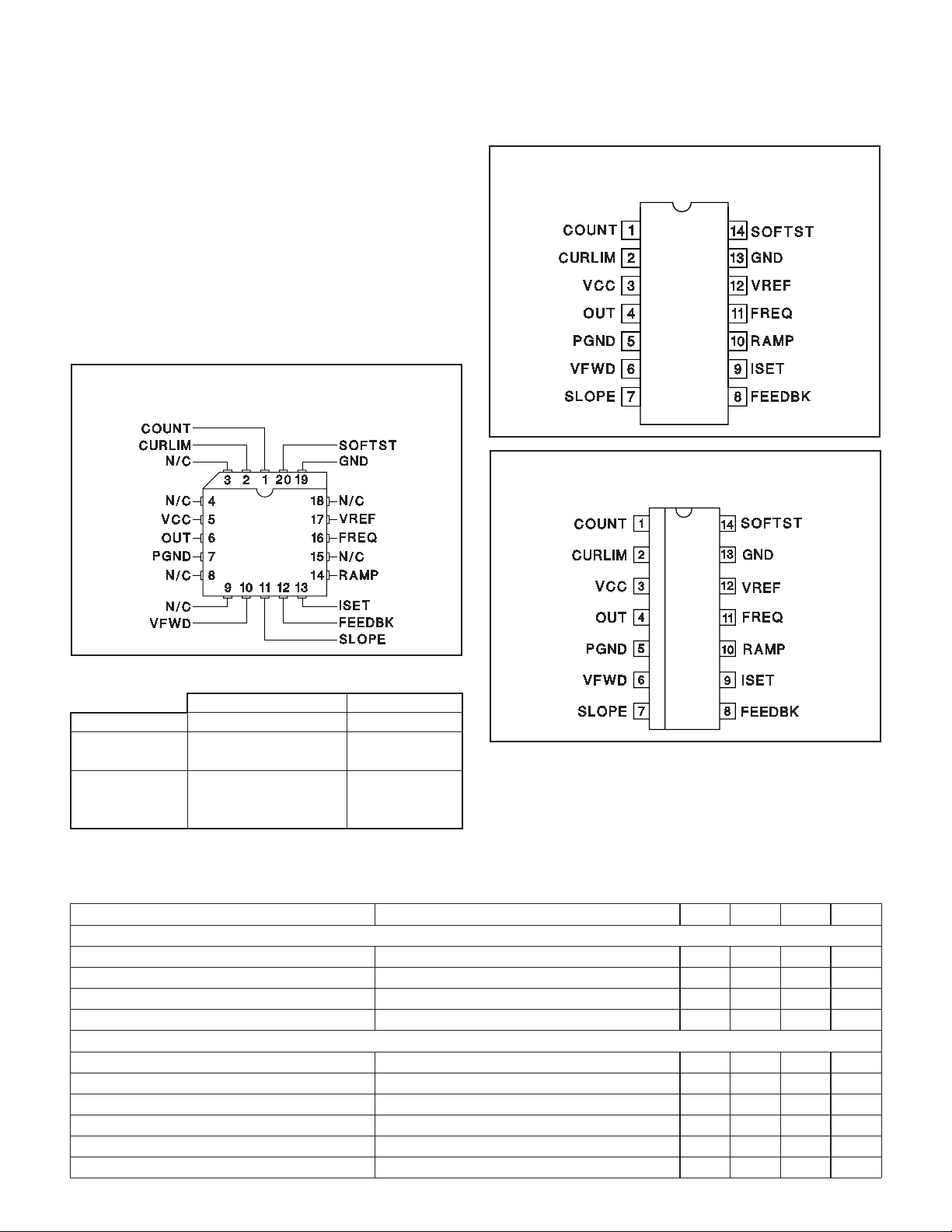
ABSOLUTE MAXIMUM RATINGS CONNECTION DIAGRAMS
Supply Voltage
(Limit Supply Current to 20mA) . . . . . . . Self Limiting at 15V
Supply Current . . . . . . . . . . . . . . . . . . . . . . . . . . . . . . . . . . . +20mA
Analog Inputs (CURLIM, VFWD, FEEBK) . . . . . . . . . . . . . . 6V
Programming Current I
Output Current I
OUT
SLOPE,IISET
. . . . . . . . . . . . . . . . . –1mA
DC . . . . . . . . . . . . . . . . . . . . . . . . . . . . . . . . . . . . . ±180mA
Pulse (0.5ms) . . . . . . . . . . . . . . . . . . . . . . . . . . . . . . . ±1.2A
Note: All voltages are with respect to GND. Currents are positive into the specified terminal. Consult Packaging Section of
Databook for thermal limitations and considerations of package.
PLCC-20 (TOP VIEW)
Q Package
DIL-14 (TOP VIEW)
N or J Package
SOIC-14 (TOP VIEW)
D Package
UCC1570
UCC2570
UCC3570
ORDERING INFORMATION
Temperature Range Package
UCC1570J –55°C to +125°C Ceramic Dip
UCC2570D –40°C to +85°C SOIC
UCC2750N Plastic Dip
UCC3570D 0°C to +70°C SOIC
UCC3570N Plastic Dip
UCC3570Q PLCC
ELECTRICAL CHARACTERISTICS: Unless otherwise stated, these specifications apply for T
UCC3570, TA= –40 to 85°C for the UCC2570, TA=–55 to 125°C for the UCC1570, R
C
=150pF, VCC=11V and TA=TJ.
RAMP
PARAMETER TEST CONDITIONS Min Typ Max Units
Reference
VREF VCC =10 to 13V, I
= 0 to 2mA 4.9 5 5.1 V
VREF
Line Regulation VCC = 10 to 13V 2 10 mV
Load Regulation I
= 0 to 2mA 2 10 mV
VREF
Short Circuit Current VREF = 0 10 50 mA
VCC
Vth (On) 12 13 V
Vth (Off) 8 9 10 V
Hysteresis 345V
VCC I
Start VCC = 11V, VCC Comparator Off 85 150 µA
I
VCC
I
VCC Run
= 10mA 13.5 15 16 V
VCC
VCC Comparator On 1 1.5 mA
ISET
=100k, R
= 0 to 70°C for the
A
=121k, C
SLOPE
FREQ
=180pF,
2
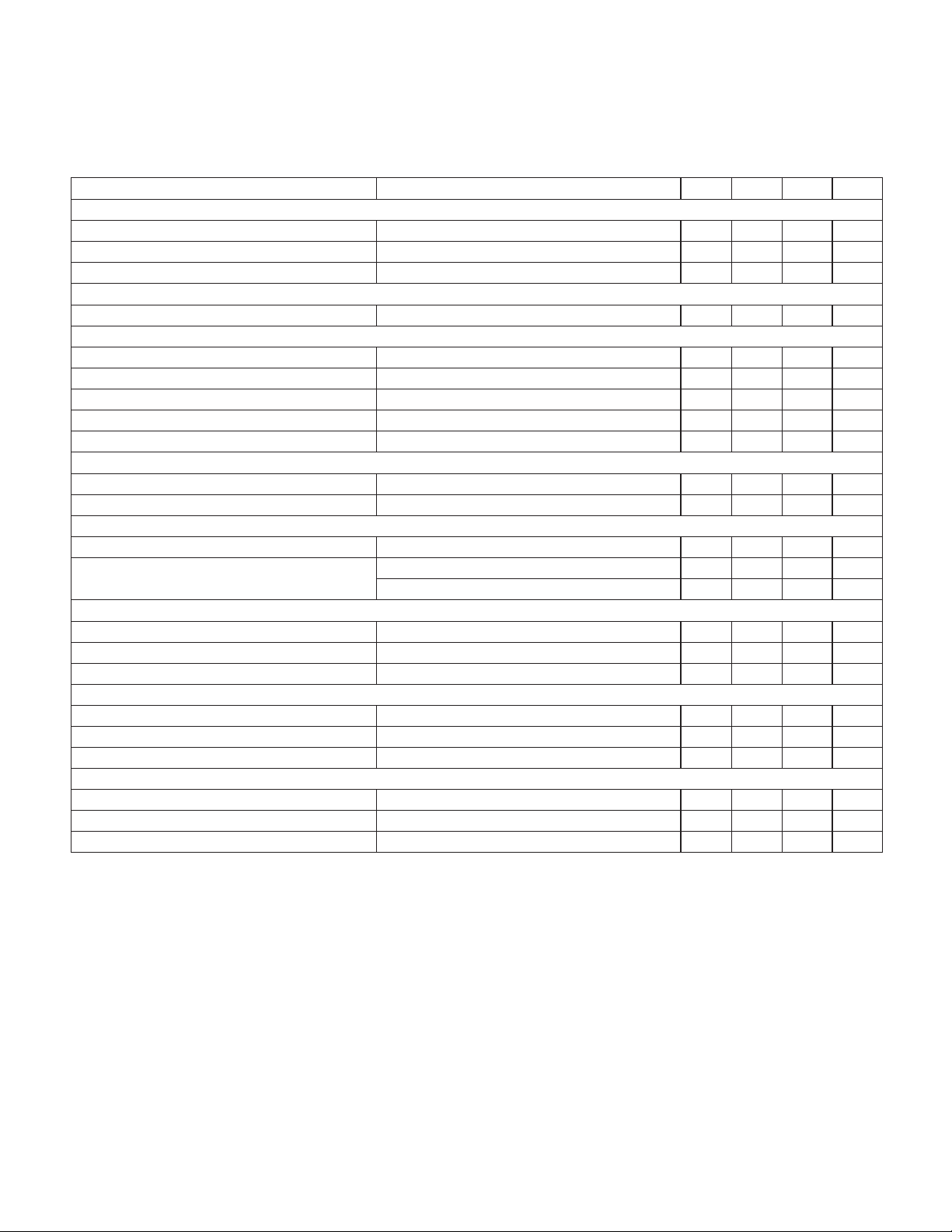
UCC1570
UCC2570
UCC3570
ELECTRICAL CHARACTERISTICS:
UCC3570, TA= –40 to 85°C for the UCC2570, TA=–55 to 125°C for the UCC1570, R
C
=150pF, VCC=11V and TA=TJ.
RAMP
PARAMETER TEST CONDITIONS Min Typ Max Units
Line Sense
Vth High Line Comparator 3.9 4 4.1 V
Vth Low Line Comparator 0.96 1 1.04 V
lib (VFWD) 0 ±100 nA
Oscillator
Frequency 90 100 110 kHz
Ramp Generator
I
RAMP/ISLOPE
–I
RAMP/IISET
Peak Ramp Voltage 3.8 4 4.2 V
Valley Ramp Voltage 0.95 1 1.05 V
ISET Voltage Level 0.95 1 1.05 V
Soft Start
Saturation VCC = 11V, VCC Comparator Off 25 100 mV
I
SOFTST/IISET
Pulse Width Modulator
lib(FEEDBK) 0 ±100 n A
FEEDBK Zero Duty Cycle 0.9 1 1.1 V
Current Limit
lib(CURLIM) 0 ±100 nA
Vth Current Limit 180 200 220 mV
Vth Shutdown 500 600 700 mV
Fault Counter
Vth 3.8 4 4.2 V
Vsat 0 100 mV
I
COUNT/IISET
Output Driver
Vsat High I
Vsat Low I
Rise/Fall Time C
Unless otherwise stated, these specifications apply for TA= 0 to 70°C for the
=100k, R
ISET
Maximum Duty Cycle, (Note 1) 3.8 4 4.2 V
= –100mA 0.4 1 V
OUT
= 100mA 0.4 1 V
OUT
= 1nF, (Note 1) 20 100 ns
OUT
=121k, C
SLOPE
9 10 11 A/A
9 10 11 A/A
0.8 1 1.2 A/A
0.8 1 1.2 A/A
FREQ
=180pF,
Note 1: This parameter guaranteed by design but not 100% tested in production.
PIN DESCRIPTIONS
VCC: Chip supply voltage pin. Bypass to PGND with a
low ESL/ESR 0.1µF capacitor plus a capacitor for gate
charge storage.Lead lengths must be minimum.
PGND: Ground pin for the output driver. Keep connections less than 2cm. Carefully maintain low impedance
path for high current return.
OUT: Gate drive output pin. Connect to the gate of a
power MOSFET with a resistor greater than 2Ω. Keep
connection lengths under 2cm.
VFWD: Voltage Feed Forward and Line Sense pin. Connect to input DC line using a resistive divider.
SLOPE: Program the charging current for RAMP with a
resistor from this pin to GND. This pin will follow VFWD.
FEEDBK: Input to the pulse width modulator comparator.
Drive this pin with an optocoupler to GND and a resistor
to VREF. Modulation input range is from 1V to 4V.
ISET: A resistor from this pin to GND programs RAMP
discharge current, FREQ current, SOFTST current, and
COUNT current.
3

PIN DESCRIPTIONS (cont.)
RAMP: Ramp Pin. Connect a capacitor to GND. Rising
slope is programmed by current in SLOPE. This slope is
compared to FEEDBK for pulse width modulation. The
falling slope is programmed by the current in ISET and
used to limit maximum duty cycle.
FREQ: Oscillator pin. Program the frequency with a capacitor to GND.
VREF: Precision 5V reference, and bypass point for internal circuitry. Bypass this pin with a 1µF minimum capacitor to GND.
APPLICATION INFORMATION
(Note: Refer to Typical Application for external component names.) All the equations given below should be
considered as first order approximations with final values
determined empirically for a specific application.
Power Sequencing
VCC normally connects through a high impedance (R5)
to the rectified line, with an additional path(R6) to a low
voltage, bootstrap on the winding power transformer.
VFWD normally connects to a divider (R1 and R2) from
the rectified line. For circuit activation, all of the following
considerations are required:
1. VFWD between 1V and 4V
2. VCC has been under 9V (to reset the shutdown
latch)
3. VCC over 13V
At this time, the circuit will activate. I
from its start up value of 85µA to its run value of 1mA.
The capacitor on SOFTST is charged with a current determined by:
V
1
–
I
SOFTST
.
=
R
4
When SOFTST rises above 1V, output pulses will begin
and I
charge requirements asI
will further rise to a level dictated by gate
VCC
≈ 1mA + QTfs. With output
VCC
pulses, the low voltage bootstrap winding should now
power the controller. If VCC falls below 9V, the controller
will turn off and the start sequence will reset and retry.
VCC Clamp
An internal shunt regulator clamps VCC so that it will not
exceed 15V.
will increase
VCC
UCC1570
UCC2570
UCC3570
GND: Analog ground. Connect to a low impedance
ground plane containing all analog low current returns.
SOFTST: Soft start pin. Program with a capacitor to
GND.
COUNT: Program the time that fault events will be toler-
ated before shutdown occurs with a capacitor and resistor to GND.
CURLIM: Current Limit Sense pin. Terminates OUT gate
drive pulse for inputs over 0.2V. Enables fault counting
function (COUNT). For inputs over 0.6V, the shutdown
latch is activated.
Output Inhibit
During normal operation, OUT is driven high at the start
of a clock period and back low when RAMP either
crosses FEEDBK or equals 4V. If, however, any of the following occur, OUT is immediately driven low for the remainder of the clock period:
1. VFWD is outside the range of 1V to 4V
2. CURLIM is greater than 0.2V
3. FEEDBK or SOFTST is less than 1V
Normal output pulses will not resume until the beginning
of the next clock period in which none of the above conditions exist.
Current Limiting
CURLIM is monitored by two internal comparators. The
current limit comparator threshold is 0.2V. If the current
limit comparator is triggered, OUT is immediately driven
low and held low for the remainder of the clock cycle,
providing pulse-by-pulse overcurrent control for excessive loads. This comparator also causes C
charged for the remainder of the clock cycle. The charging current is
V
1
–
I
COUNT
.
=
R
4
If repetitive cycles are terminated by the current limit
comparator causing COUNT to rise above 4V, the shutdown latch is set. The COUNT integration delay feature
will be bypassed by the shutdown comparator which has
a 0.6V threshold. The shutdown comparator immediately
sets the shutdown latch. R
in parallel with CFresets the
F
COUNT integrator following transient faults. R
44
•
R
greater than
()
1
−
D
()
.
MAX
F to be
must be
F
4

APPLICATION INFORMATION (cont.)
Latched Shutdown
If CURLIM rises above 0.6V, or COUNT rises to 4V, the
shutdown latch will be set. This will force OUT low, discharge SOFTST and COUNT, and reduce I
proximately 1mA. When, and if, VCC falls below 9V, the
shutdown latch will reset and I
will fall to 85µA, allow-
VCC
ing the circuit to restart. If VCC remains above 9V, an alternate restart will occur if VFWD is momentarily reduced
below 1V. External shutdown commands from any source
may be added into either the COUNT or CURLIM pins.
Deadtime Control
The voltage waveform on RAMP has independently controlled rising and falling edges. At the start of the clock
period, RAMP is at 1V and rises to 4V. It then discharges
back to 1V and awaits the next clock period. OUT can
only be high during the rising part of the waveform, while
it is positively blanked off during the falling portion. Setting the –dV/dt slope by R4 from ISET to GND establishes a minimum deadtime as:
td R C
=••03 4.
R
VCC
to ap-
UCC1570
UCC2570
UCC3570
Choose R4 between 20k and 200k and C
50pF. In order to have a pulse at OUT in the next clock
period, RAMP must fall to 1V prior to the end of the current period. If it does not, OUT will remain low for the entire next clock period.
Voltage Feedforward
The +dV/dt on RAMP is made proportional to line voltage.The slope is:
dV
dt
=•
VFWD
10
RC
•
3
()
R
where VFWD is line voltage scaled by R1 and R2. Therefore, a changing line voltage will accomplish an immediate proportionate pulse width change without any action
from the feedback amplifier. This will result in constant
volt-second drive to the power transformer providing both
international voltage operation, and excellent dynamic
line regulation. VFWD is intended to operate over a 4:1
range (1V to 4V) with undervoltage and overvoltage sensors designed to drive OUT low if this range is exceeded.
Choose R3 between 20k and 200k.
R greater than
Figure 1. UCC1570 typical application.
5

APPLICATION INFORMATION (cont.)
Frequency Set
A capacitor from FREQ to GND will determine a constant
clock frequency. Frequency is:
F
If required, frequency can be trimmed down from the
above equation by the addition of R
The reduction in frequency is a function of the ratio of
R4. RTshould be greater than 2.4 • R4 for reliable op-
R
T/
eration.
External synchronization can be accomplished by cou-
pling a narrow pulse to a resistor inserted in series with
the ground side of C
R4/200 and the synchronizing pulse width should be less
than 5% of the oscillator period.
External synchronization can also be accomplished by
driving FREQ with an CMOS inverter. The inverter must
184.
=
RC
•
()
T
from FREQ to GND.
T
The value should be less than
T.
UCC1570
UCC2570
UCC3570
be able to sink (4 • I4) with at a voltage less than the
3.5V upper threshold of the oscillator. It must also be
able to source 36 • I4 at a voltage greater than the 1.5V
lower threshold of the oscillator. As long as FREQ is held
high, the output is guaranteed to be low.
Gate Drive Output
The UCC1570 is capable of 1A peak output current. Bypass VCC with at least 0.1µF directly to PGND. Use a
capacitor with low equivalent series resistance and inductance. The connection from OUT to the MOSFET
gate should have a 2Ω or greater damping resistor and
the length should be minimized. A low impedance connection must be established between the MOSFET
source (or the ground side of the current sense resistor),
the VCC bypass capacitor and PGND. PGND should
then be connected by a single path (shown as RGND in
the application) to GND.
CLOCK
FEEDBK
RAMP
OUT
HIGH V
IN
Figure 2. Ramp and PWM waveforms.
LOW V
IN
FAULT V
IN
6

APPLICATION INFORMATION (cont.)
Figure 3. Clock generator.
UCC1570
UCC2570
UCC3570
Figure 4. External clock synchronization.
Figure 5. Frequency dependence on RT/ R4 ratio.
7

APPLICATION INFORMATION (cont.)
UCC1570
UCC2570
UCC3570
UNITRODE CORPORATION
7 CONTINENTAL BLVD. • MERRIMACK, NH 03054
TEL. (603) 424-2410 FAX (603) 424-3460
8

IMPORTANT NOTICE
T exas Instruments and its subsidiaries (TI) reserve the right to make changes to their products or to discontinue
any product or service without notice, and advise customers to obtain the latest version of relevant information
to verify, before placing orders, that information being relied on is current and complete. All products are sold
subject to the terms and conditions of sale supplied at the time of order acknowledgement, including those
pertaining to warranty, patent infringement, and limitation of liability.
TI warrants performance of its semiconductor products to the specifications applicable at the time of sale in
accordance with TI’s standard warranty. Testing and other quality control techniques are utilized to the extent
TI deems necessary to support this warranty . Specific testing of all parameters of each device is not necessarily
performed, except those mandated by government requirements.
CERTAIN APPLICATIONS USING SEMICONDUCTOR PRODUCTS MAY INVOLVE POTENTIAL RISKS OF
DEATH, PERSONAL INJURY, OR SEVERE PROPERTY OR ENVIRONMENTAL DAMAGE (“CRITICAL
APPLICATIONS”). TI SEMICONDUCTOR PRODUCTS ARE NOT DESIGNED, AUTHORIZED, OR
WARRANTED TO BE SUITABLE FOR USE IN LIFE-SUPPORT DEVICES OR SYSTEMS OR OTHER
CRITICAL APPLICA TIONS. INCLUSION OF TI PRODUCTS IN SUCH APPLICATIONS IS UNDERST OOD TO
BE FULLY AT THE CUSTOMER’S RISK.
In order to minimize risks associated with the customer’s applications, adequate design and operating
safeguards must be provided by the customer to minimize inherent or procedural hazards.
TI assumes no liability for applications assistance or customer product design. TI does not warrant or represent
that any license, either express or implied, is granted under any patent right, copyright, mask work right, or other
intellectual property right of TI covering or relating to any combination, machine, or process in which such
semiconductor products or services might be or are used. TI’s publication of information regarding any third
party’s products or services does not constitute TI’s approval, warranty or endorsement thereof.
Copyright 1999, Texas Instruments Incorporated
 Loading...