

Programmable, Off-Line, PWM Controller
DESCRIPTI ONFEATURES
• All Control, Driving, Monitoring, and
Protection Functions Included
• Low-current, Off-line Start Circuit
• Voltage Feed Forward or Current
Mode Control
• Guaranteed Duty Cycle Clamp
• PWM Latch for Single Pulse per Period
• Pulse-by-Pulse Current Limiting Plus
Shutdown for Over-Current Fault
• No Start-up or Shutdown Transients
• Slow Turn-on Both Initially and After
Fault Shutdown
• Shutdown Upon Over- or
Under-Voltage Sensing
• Latch Off or Continuous Retry After
Fault
• PWM Output Switch Usable to 1A
Peak Current
• 1% Reference Accuracy
• 500kHz Operation
• 18 Pin DIL Package
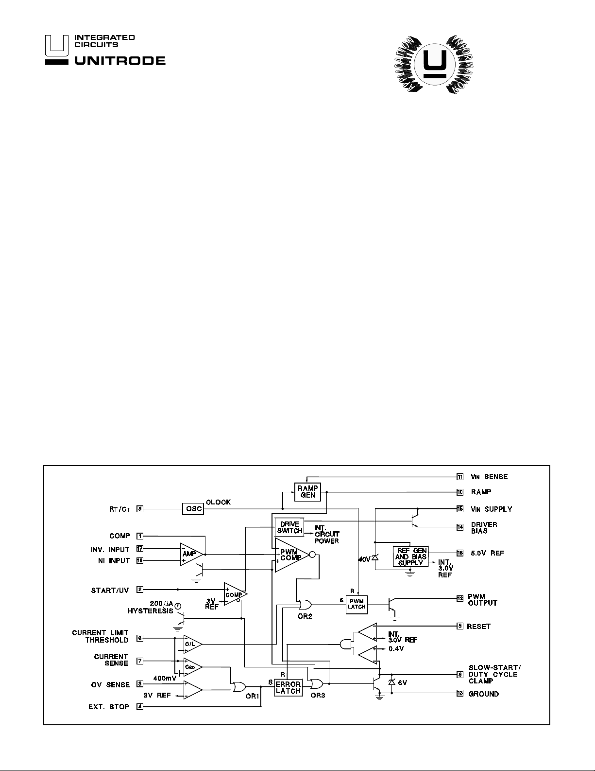
BLOCK DIAGRA M
The UC1841 family of PWM controllers has been designed to increase
the level of versatility while retaining all of the performance features of
the earlier UC18 40 de vices. While still optimized for highly-efficient bootstrapped pri mary-side operati on in forward or flyback power converters,
the UC1841 is equall y adept in impl ementing b oth low a nd high voltage
input DC to DC converters. Important performance features include a
low-current starting circuit, linear feed-forward for constant volt-second
operation, and compatibility with either voltage or current mode topologies.
In addition to start-up and normal regulating PWM functions, these devices include built in protection from over-voltage, under-voltage, and
over-current fault conditions with the option for either latch-of f or automatic restart.
While pin compatib le with the UC1840 in all respects except that the polarity of the External Stop has bee n re versed, the UC1841 offers the following improvements:
1. Fault latch reset is accomplished with slow start discharge rather
than recycling the input voltage to the chip.
2. The External Stop input can be used for a fault delay to resist
shutdown from short durat ion transients.
3. The duty-cycle clamping function has been characterized an d
specified.
The UC1841 is characteri zed for -55°C to +125°C operation while the
UC2841 and UC3841 are desi gned for -25°C to +85°C and 0°to +70°C,
respectively.
UC1841
UC2841
UC3841
Note: Positive tru e lo gic, latch output s high wit h set, reset has prior ity.
6/93
ABSOLUTE MAXI MUM RATING S
Supply Voltage, +VIN (Pin 15) (Note 2)
Voltage Driven. . . . . . . . . . . . . . . . . . . . . . . . . . . . . . . . . +32V
Current Drive n, 100mA maximum. . . . . . . . . . . . Self-limiting
PWM Output Volta ge (Pin 12 ) . . . . . . . . . . . . . . . . . . . . . . . 40V
PWM Out put Current, Steady-State (Pin 12). . . . . . . . . 400mA
PWM Output Peak Energy Disc harge . . . . . . . . . . . . 20 µJo ules
Driver Bias Current (Pin 14). . . . . . . . . . . . . . . . . . . . . -200mA
Reference Output Current (Pin 16) . . . . . . . . . . . . . . . . -50mA
Slow-Start Sink Curren t (Pin 8) . . . . . . . . . . . . . . . . . . . . 20mA
V
IN Sense Current (Pin 11). . . . . . . . . . . . . . . . . . . . . . . . 10mA
Current Limit Input s (Pins 6 & 7) . . . . . . . . . . . . . -0.5 to +5.5V
Stop Input (Pin 4) . . . . . . . . . . . . . . . . . . . . . . . . . -0.3 to +5. 5V
Compara to r Inputs
(Pins 1, 7, 9-1 1, 1 6). . . . . . . . . . . . Internally clamp ed at 12V
Power Dissipation at T
Power Dissipation at T
A = 25°C (Note 3) . . . . . . . . . . . 1000mW
C = 25°C (Note 3). . . . . . . . . . . 2000mW
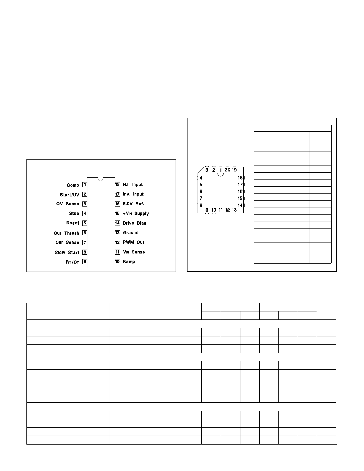
CONNECTION DIAGRAMS
DIL-18, SOIC- 18 (T O P VIEW)
J or N, DW Package
UC1841
UC2841
UC3841
Operating Junct ion Te mp era tu re . . . . . . . . . . -55°C to +150°C
Storage Temperature Range. . . . . . . . . . . . . . -65°C to +150°C
Lead Temp era ture (Solder in g, 10 sec). . . . . . . . . . . . . +300°C
Note 1: All voltages are with respect to ground, Pin 13.
Currents are positiv e-int o, negat ive-o ut of the specif ie d
terminal.
Note 2: All p in num ber s are refer ence d to DIL- 18 pa ckag e.
Note 3: C on sult Packag in g Section of Dat aboo k for ther ma l
limitations and cons id era tion s of packa ge.
PLCC-20, LCC-20
(TOP VIEW)
Q or L Package
PACKAGE PIN FUNCTIONS
FUNCTION PIN
Comp 1
Start/UV 2
OV Sense 3
Stop 4
Reset 5
CUR Thresh 7
CUR Sense 8
Slow Start 9
R
T/CT 10
Ramp 11
V
IN Sense 12
PWM Out 13
Ground 14
Drive Bias 15
+V
IN Supply 17
5.0V REF 18
Inv. Input 19
N.I. Inpu t 20
ELECTRICAL CHARACTERISTICS:
UC1841, -25°C to +85°C for the UC2841, and 0°C to +70 °C for the UC3841; V
C
R = .001mfd, Current Lim it Thres hold = 200 mV, TA = TJ.
Unless otherwise stated , these spec ificat ions apply for TA = -55°C to +125°C for the
IN = 20V, RT = 20k Ω , CT = .001mfd, RR = 10kΩ,
UC1841 / UC2841 UC3841 UNITS
PARAMETER TEST CONDITIONS
MIN TYP MAX MIN TYP MAX
Power Inputs
Start-Up Curr ent V
Operating Cur ren t V
Supply OV Clamp I
IN = 30V, Pin 2 = 2.5V 4.5 6 4.5 6 mA
IN = 30V, Pin 2 = 3.5V 10 14 10 14 mA
IN = 20mA 33 40 45 33 40 45 V
Reference Sec tio n
Reference Voltage T
Line Regulatio n V
Load Regulation I
J = 25°C 4.95 5.0 5.05 4.9 5.0 5.1 V
IN = 8 to 30V 10 15 10 20 mV
L = 0 to 10mA 1020 1030mV
Temperature Stability Over Operating Temper ature Range 4.9 5.1 4 .8 5 5.15 V
Short Circuit Current V
REF = 0, TJ
= 25°C -80 -100 -80 -100 mA
Oscillator
J
Nominal Frequency T
Voltage Stability V
= 25°C 47 50 53 45 50 55 kHz
IN = 8 to 30V 0.5 1 0.5 1 %
Temperature Stability Over Operating Temper ature Range 45 55 43 57 kHz
Maximum Frequency R
T = 2kΩ, CT = 330pF 500 500 kHz
2
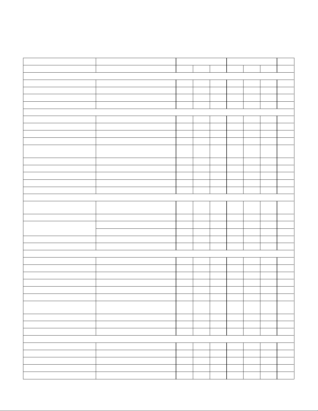
ELECTRICAL CHARACTERISTICS:
UC1841, -25°C to +85°C for the UC2841, and 0°C to +70 °C for the UC3841; V
C
R = .001mfd, Current Limit Thresh old = 200mV, TA = TJ.
Unless otherwise stated , these spec ificat ions apply for TA = -55°C to +125°C for the
IN = 20V, RT = 20k Ω , CT = .001mfd, RR = 10kΩ,
PARAMETER TEST CONDITIONS UC1841 / UC2841 UC3841 UNITS
MIN TYP MAX MIN TYP MAX
Ramp Ge nerator
Ramp Curren t, M in imum I
Ramp Current, M axim um I
SENSE = -10µA -11 -14 -11 -14 µA
SENSE = 1.0mA -0.9 -.95 -0.9 -.95 mA
Ramp Valley 0.3 0.4 0.6 0.3 0.4 0.6 V
Ramp Peak Clamp ing Leve l 3.9 4.2 4.5 3.9 4.2 4.5 V
Error Amplifier
Input Offs et Vo lta ge V
CM = 5.0V 0.5 5 2 10 mV
Input Bias Cur rent 0.5 2 1 5 µA
Input Offs et Cu rr ent 0.5 0.5 µA
Open Loop Gain ∆V
Output Swing (Max. Output ≤
O= 1 to 3V 60 66 60 66 dB
Minimum Total Range 0.3 3.5 0.3 3.5 V
Ramp Peak - 100mV)
CMRR V
PSRR V
Short Circuit Current V
Gain Bandwidth* T
Slew Rate* T
CM = 1.5 to 5.5V 70 80 70 80 dB
IN = 8 to 30V 70 80 70 80 dB
COMP = 0V -4 -10 -4 -10 mA
J = 25°C, AVOL = 0dB 1 2 1 2 MHz
J = 25°C, AVCL
= 0dB 0.8 0.8 V/µs
PWM Section
Continuous Duty Cycle
Range* (other than zero)
50% Duty Cycle Clamp R
Output Saturation I
Output Lea kage V
Comparator Dela y* Pin 8 to Pin 12, T
Minimum Total Cont inuou s Range,
495495%
Ramp Peak < 4.2V
SENSE to VREF = 10k 42 47 52 42 47 52 %
OUT = 20mA 0.2 0.4 0.2 0.4 V
I
OUT = 200mA 1. 7 2. 2 1.7 2.2 V
OUT = 40V 0.1 10 0. 1 10 µA
J = 25°C, RL = 1kΩ 300 500 300 500 ns
Sequencing Functions
Comparator Thre sholds P ins 2, 3, 5 2.8 3.0 3.2 2.8 3.0 3.2 V
Input Bias Curren t Pins 3, 5 = 0V -1.0 -4.0 -1.0 -4.0 µA
Input Leakage Pins 3, 5 = 10V 0.1 2.0 0.1 2.0 µA
Start/UV Hyster esis Cur ren t Pin 2 = 2.5V 170 200 220 1 70 200 23 0 µA
Ext. Stop Threshold Pin 4 0.8 1.6 2.4 0.8 1.6 2.4 V
Error Latch Activat e Cur ren t Pin 4 = 0V, Pin 3 > 3V -120 -20 0 -120 -20 0 µA
Driver Bias Saturation Volta ge,
V
IN - VOH
Driver Bias Leakage V
Slow-Start Saturation I
Slow-Start Leakage V
IB = -50mA 2 3 2 3 V
B = 0V -0.1 -10 -0.1 -10 µA
S = 10mA 0.2 0.5 0.2 0.5 V
S = 4.5V 0.1 2.0 0.1 2.0 µA
Current Control
Current Limit Off set 0 5 0 10 mV
Current Shutdown O ffs et 370 400 430 360 400 440 mV
Input Bias Current Pin 7 = 0V -2 -5 -2 -5 µA
Common Mode Range* -0.4 3.0 -0.4 3.0 V
Current Limit Delay* T
J = 25°C, Pin 7 to 12, RL = 1k 200 400 200 400 ns
* These paramet ers are guara nt eed by design bu t not 100% teste d in prod uct ion.
UC1841
UC2841
UC3841
3
FUNCTIONAL DES CRIP TIO N
PWM CONTROL
1. Oscillator Gen era te s a fixed-frequency int er nal clock fro m an extern al R
K
Frequency =
C
where KC is a first order correction factor ≈ 0.3 log (CT X 1012).
RTCT
UC1841
UC2841
UC3841
T and CT.
2. Ramp Gener ator
Develops a linear ramp with a slope defined exter nally by
dv
dt
=
sense
R
voltage
RCR
CR is normally se le ct ed ≤ CT and its value will have some effect upon va lley volta ge.
Limiting the minimum value for I
C
R terminal can be used as an input port for curren t mode cont rol.
SENSE will establish a maximum duty cycle clamp .
3. Error Amplifier Conventional operation al amp lifier f or closed- loop ga in and phase com pe nsat ion.
Low output impedance; unity-gain stable.
The output is held low by the slow star t voltag e at turn on in order to minimize over shoo t.
4. Reference Ge n era tor Precision 5.0V for internal and extern al usage to 50mA.
Tracking 3.0V ref er enc e for intern al usage only w ith nomina l accur acy of
± 2%.
40V clamp zener for chip OV prot ect ion, 100m A m axim um current .
5. PWM Comparat or Gen era tes out put pulse which start s at term inat ion of clock pulse and ends whe n the ram p
input crosses the lowest of two posit iv e input s.
6. PWM Latch Terminat es the PW M output pulse whe n set by inputs fro m either th e PWM com pa rator , the
pulse-by-p ulse cur re nt limit compa rator , or the error latch. Reset s with each inter nal clock
pulse.
7. PWM Output Switch Transisto r capable of sinking cu rrent to ground which is of f during the PWM on- tim e and turns
on to terminate the power pulse. Curr ent cap acit y is 400mA sat ur ated with peak
capacitanc e discharge in excess of one am p.
SEQUENCING FUNCTIONS
1. Start/UV Sense With an increasing vo lta g e, it gene rates a turn-on signa l an d releases t he slow- star t clamp at
a start threshold.
With a decreasing volta ge, it genera tes a turn- of f com mand at a lower leve l separ at ed by a
200
µA hystere sis cur ren t.
2. Drive Switch Disab le s most of the chip to hold internal curre nt consump tion low, and Driver Bias OF F, unt il
input voltage reaches start threshold.
3. Driver Bias Supplies drive current to exter nal power switch to prov ide tu rn-on bias .
4. Slow Start Clamps low to hold PWM OFF. Upon release, rises with rate contro lled by R
SCS for slow
increase of output pulse widt h.
Can also be used as an alt ernate maximum duty cycle clamp wit h an ext er nal volt age divider.
PROTECTION FUNCTIO NS
1. Error Latch When set by mome nt ary input , this latch insur es im me diat e PWM shu tdown and hold of f until
reset. Inputs to Error Latch are :
a. OV > 3.2V (typically 3V)
b. Stop > 2.4V (typically 1.6V)
c. Current Sense 400mV ov er thresho ld (typical) .
Error Latch reset s whe n slow start voltage falls to 0.4V if Rese t Pin 5 < 2.8V. Wit h Pin 5 >
3.2V, Error Latch will remain set.
2. Current Limiting Differential input comparator terminat es individual output pulses each t ime sense voltage
rises above thre shold.
When sense volta ge rise s to 400m V (typica l) abov e thres hold, a shutdo wn signal is sent t o
Error Latch.
3. External Stop A voltage over 1.2 V will set the Erro r Latch and hold the ou tp ut off.
A voltage less than 0. 8V w ill defe a t the error latch and prevent shutd o wn.
A capacitor here will slow the action of the erro r latch for tra nsient prot ection by providing a
typical delay of 13ms/
µF.
4
UC1841
UC2841
UC3841
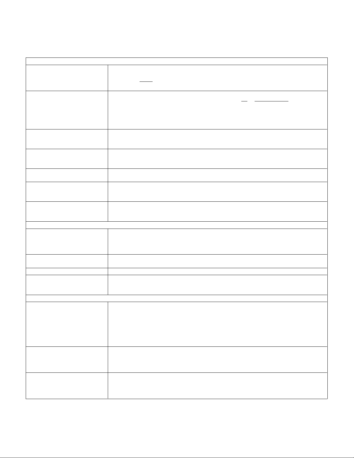
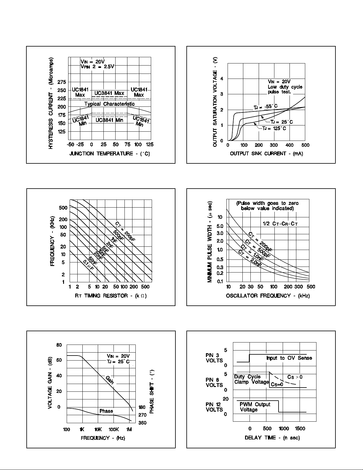
Start/UV Hysteresis
PWM Output-Saturation Voltage
PWM Output Minimu m Pu lse W idthOscillator Frequency
Shutdown TimingError Amplifier Op en Loop Gain an d Phase
5
 Loading...