

Texas Instruments CD74HCT423M96, CD74HCT423E, CD74HCT123M96, CD74HCT123M, CD74HCT123E Datasheet
...
Data sheet acquired from Harris Semiconductor
/
j
SCHS142
September 1997
CD74HC123, CD74HCT123,
CD74HC423, CD74HCT423
High Speed CMOS Logic Dual Retriggerable
Monostable Multivibrators with Resets
[ /Title
(CD74
HC123
,
CD74
HCT12
3,
CD74
HC423
,
CD74
HCT42
3)
Subect
(High
Speed
Features
• Overriding Reset Terminates Output Pulse
• Triggering From the Leading or Trailing Edge
• Q and
• Separate Resets
• Wide Range of Output-Pulse Widths
• Schmitt Trigger on Both
• Fanout (Over Temperature Range)
• Wide Operating Temperature Range . . . -55
• Balanced Propagation Delay and Transition Times
• Significant Power Reduction Compared to LSTTL
• HC Types
• HCT Types
Q Buffered Outputs
A and B Inputs
- Standard Outputs. . . . . . . . . . . . . . . 10 LSTTL Loads
- Bus Driver Outputs . . . . . . . . . . . . . 15 LSTTL Loads
o
C to 125oC
Logic ICs
- 2V to 6V Operation
- High NoiseImmunity: N
V
= 5V
CC
= 30%, NIH= 30%of VCCat
IL
- 4.5V to 5.5V Operation
- Direct LSTTL Input Logic Compatibility,
V
= 0.8V (Max), VIH = 2V (Min)
IL
- CMOS Input Compatibility, I
≤ 1µA at VOL, V
l
OH
Description
The Harris CD74HC123, CD74HCT123, CD74HC423 and
CD74HCT423 are dual monostable multivibrators with
resets. They are all retriggerable and differ only in that the
123 types can be triggered by a negative to positive reset
pulse; whereas the 423 types do not have this feature. An
external resistor (R
) and an external capacitor (CX) control
X
the timing and the accuracy for the circuit. Adjustment of Rx
and C
the Q and
provides a wide range of output pulse widths from
X
Q terminals. Pulse triggering on the A and B
inputs occur at a particular voltage level and is not related to
the rise and fall times of the trigger pulses.
Once triggered, the output pulse width may be extended by
retriggering inputs
A and B. The output pulse can be
terminated by a LOW level on the Reset (R) pin. Trailing
edge triggering (
A) and leading edge triggering (B) inputs
are provided for triggering from either edge of the input
pulse. If either Mono is not used each input on the unused
device (
A, B, and R) must be terminated high or low.
The minimum value of external resistance, Rx is typically 5kΩ.
The minimum value external capacitance, C
calculation for the pulse width is t
= 0.45 RXCX at VCC = 5V.
W
, is 0pF. The
X
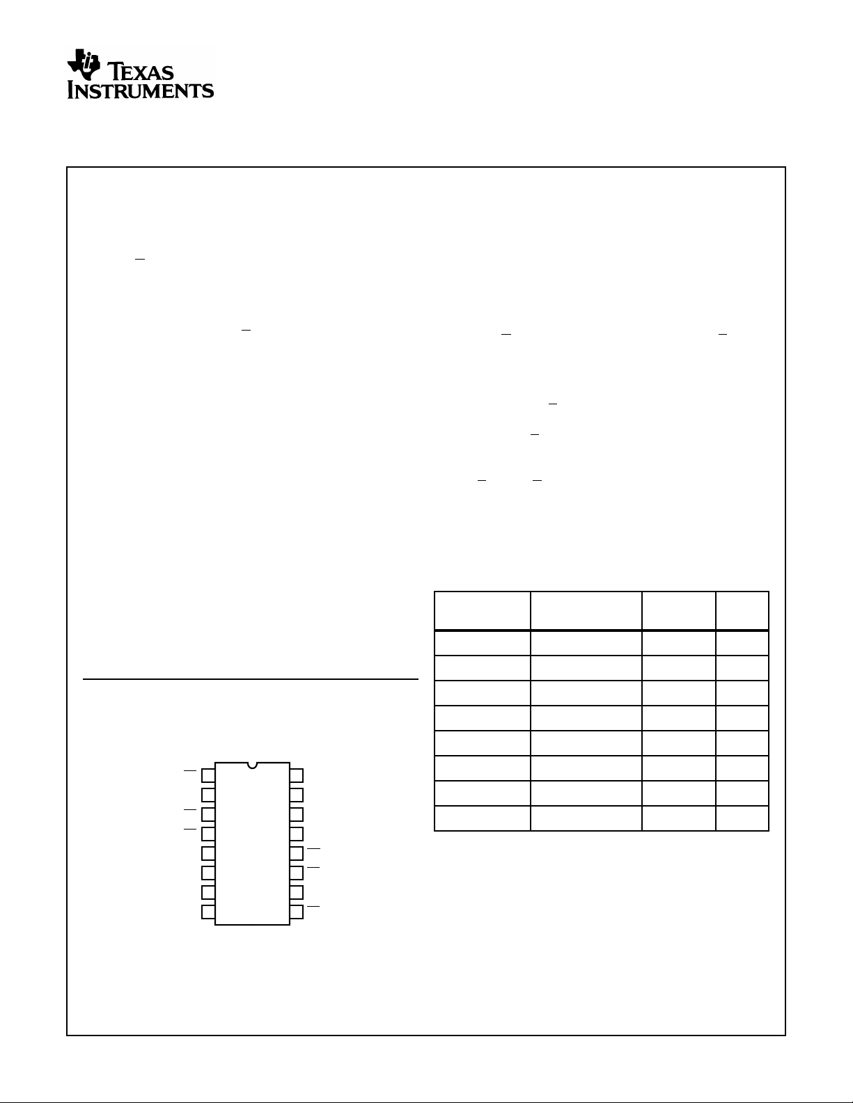
Ordering Information
PKG.
PART NUMBER TEMP. RANGE (oC) PACKAGE
CD74HC123E -55 to 125 16 Ld PDIP E16.3
CD74HCT123E -55 to 125 16 Ld PDIP E16.3
NO.
Pinout
CD74HC123, CD74HCT123, CD74HC423, CD74HCT423
(PDIP, SOIC)
TOP VIEW
16
1
1A
2
1B
3
1R
4
1Q
5
2Q
6
2C
X
2R
7
XCX
8
GND
CAUTION: These devices are sensitive to electrostatic discharge. Users should follow proper IC Handling Procedures.
Copyright
© Harris Corporation 1997
V
CC
15
1R
XCX
14
1C
X
13
1Q
12
2Q
11
2R
10
2B
9
2A
CD74HC423E -55 to 125 16 Ld PDIP E16.3
CD74HCT423E -55 to 125 16 Ld PDIP E16.3
CD74HC123M -55 to 125 16 Ld SOIC M16.15
CD74HCT123M -55 to 125 16 Ld SOIC M16.15
CD74HC423M -55 to 125 16 Ld SOIC M16.15
CD74HCT423M -55 to 125 16 Ld SOIC M16.15
NOTES:
1. When ordering, use the entire part number. Add the suffix 96 to
obtain the variant in the tape and reel.
2. Wafer ordiefor this partnumber is availablewhichmeets all electrical specifications. Please contact your local sales office or
Harris customer service for ordering information.
1
File Number 1708.1
CD74HC123, CD74HCT123, CD74HC423, CD74HCT423
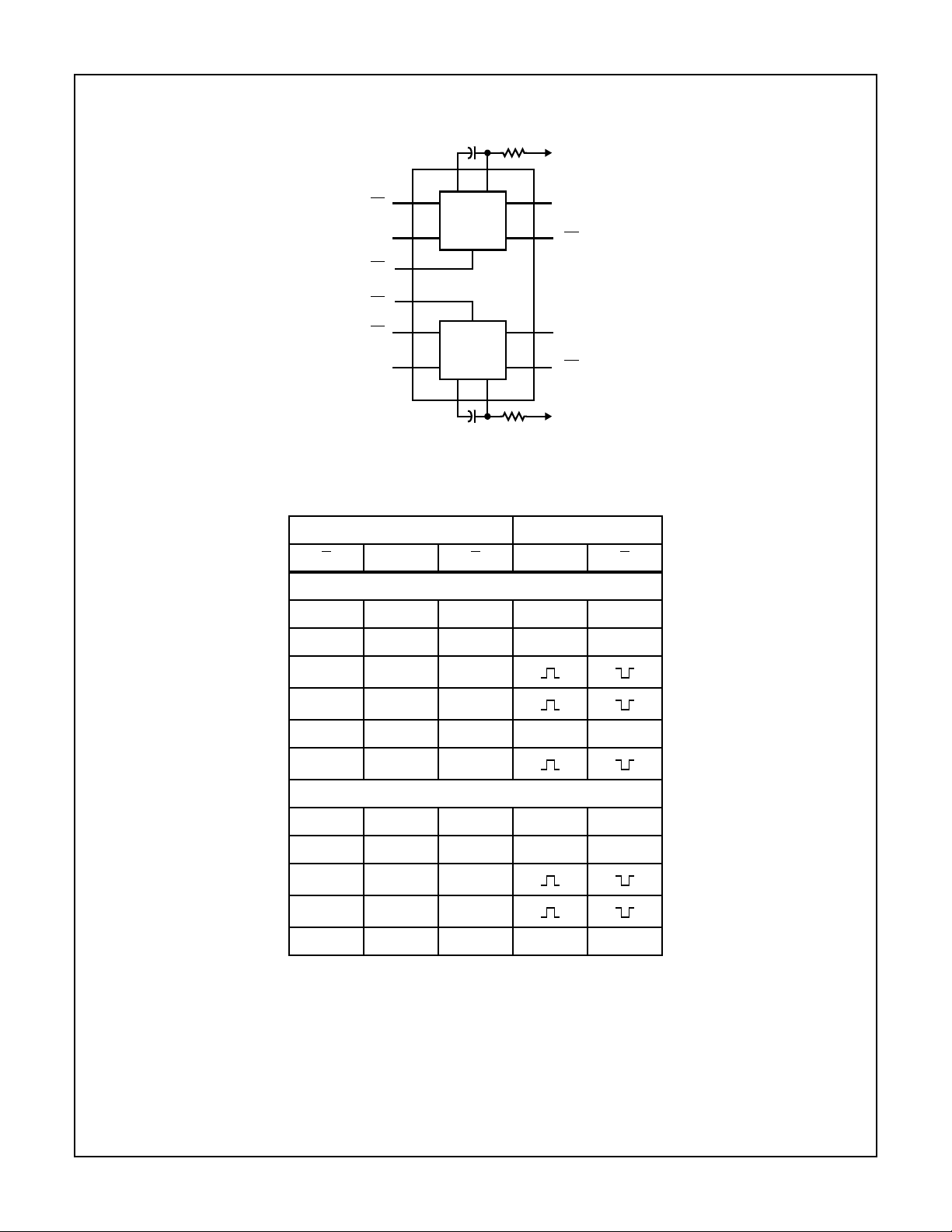
Functional Diagram
1A
1B
1R
2R
2A
2B
14 15
1Cx 1RxCx
1
2
3
11
9
10
MONO 1
MONO 2
2Cx 2RxCx
67
1Cx 1Rx
2Cx 2Rx
V
13
4
5
12
V
TRUTH TABLE
INPUTS OUTPUTS
ABRQQ
CD74HC/HCT123
CC
1Q
1Q
2Q
2Q
CC
HXHLH
XLHLH
L ↑ H
↓ HH
XXLLH
LH↑
CD74HC/HCT423
HXHLH
XLHLH
L ↑ H
↓ HH
XXLLH
NOTE: H = High Voltage Level, L = Low Voltage Level,
X = Don’t Care.
2
CD74HC123, CD74HCT123, CD74HC423, CD74HCT423
Absolute Maximum Ratings Thermal Information
DC Supply Voltage, VCC. . . . . . . . . . . . . . . . . . . . . . . . -0.5V to 7V
DC Input Diode Current, I
IK
For VI < -0.5V or VI > VCC + 0.5V. . . . . . . . . . . . . . . . . . . . . .±20mA
DC Output Diode Current, I
OK
For VO < -0.5V or VO > VCC + 0.5V . . . . . . . . . . . . . . . . . . . .±20mA
DC Output Source or Sink Current per Output Pin, I
O
For VO > -0.5V or VO < VCC + 0.5V . . . . . . . . . . . . . . . . . . . .±25mA
DC VCC or Ground Current, I
CC orIGND
. . . . . . . . . . . . . . . . . .±50mA
Operating Conditions
Temperature Range (TA) . . . . . . . . . . . . . . . . . . . . . -55oC to 125oC
Supply Voltage Range, V
HC Types . . . . . . . . . . . . . . . . . . . . . . . . . . . . . . . . . . . . .2V to 6V
HCT Types . . . . . . . . . . . . . . . . . . . . . . . . . . . . . . . . .4.5V to 5.5V
DC Input or Output Voltage, VI, VO . . . . . . . . . . . . . . . . . 0V to V
Input Rise and Fall Time
2V . . . . . . . . . . . . . . . . . . . . . . . . . . . . . . . . . . . . . . 1000ns (Max)
4.5V. . . . . . . . . . . . . . . . . . . . . . . . . . . . . . . . . . . . . . 500ns (Max)
6V . . . . . . . . . . . . . . . . . . . . . . . . . . . . . . . . . . . . . . . 400ns (Max)
CAUTION: Stresses above those listed in “Absolute Maximum Ratings” may cause permanent damage to the device. This is a stress only rating and operation
of the device at these or any other conditions above those indicated in the operational sections of this specification is not implied.
NOTE:
3. θJA is measured with the component mounted on an evaluation PC board in free air.
CC
Thermal Resistance (Typical, Note 3) θJA (oC/W)
PDIP Package. . . . . . . . . . . . . . . . . . . . . . . . . . . . . 90
SOIC Package. . . . . . . . . . . . . . . . . . . . . . . . . . . . . 115
Maximum Junction Temperature. . . . . . . . . . . . . . . . . . . . . . .150oC
Maximum Storage Temperature Range . . . . . . . . . .-65oC to 150oC
Maximum Lead Temperature (Soldering 10s). . . . . . . . . . . . .300oC
(SOIC - Lead Tips Only)
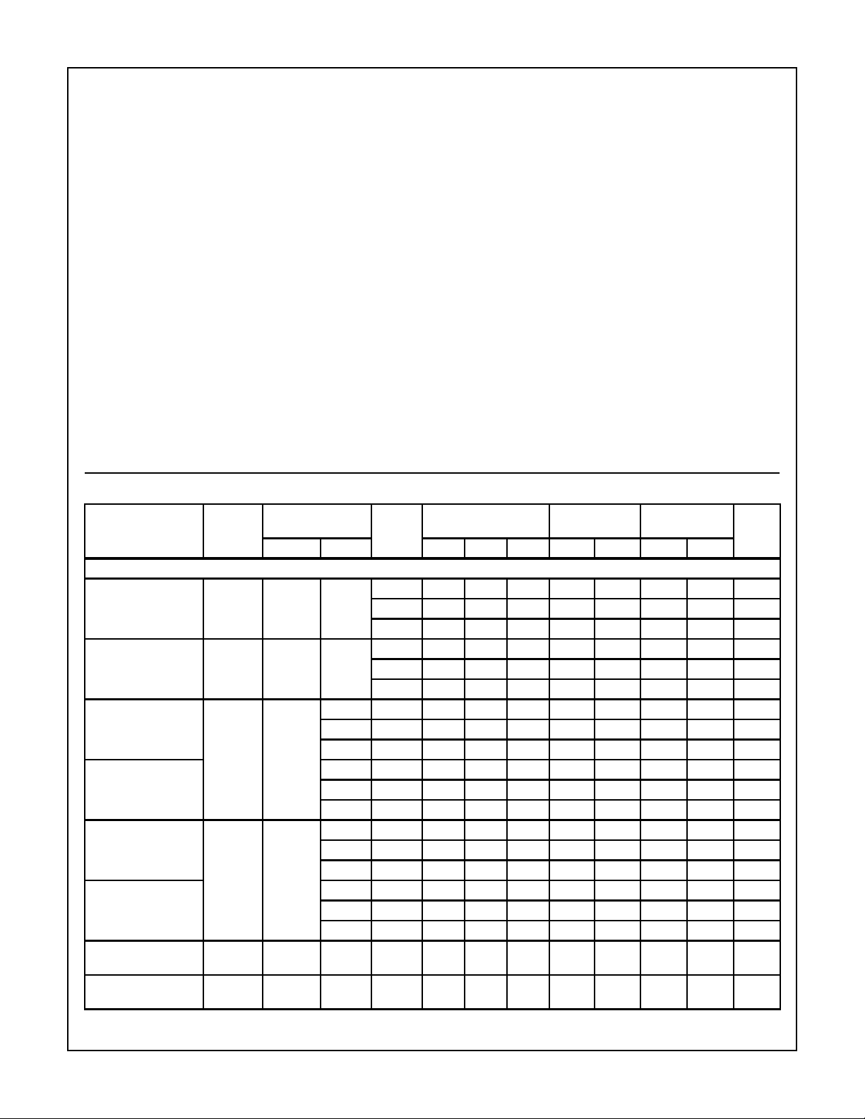
CC
DC Electrical Specifications
PARAMETER SYMBOL
HC TYPES
High Level Input
Voltage
Low Level Input
Voltage
High Level Output
Voltage
CMOS Loads
High Level Output
Voltage
TTL Loads
Low Level Output
Voltage
CMOS Loads
Low Level Output
Voltage
TTL Loads
Input Leakage
Current
Quiescent Device
Current
V
IH
V
IL
V
OH
V
OL
I
I
I
CC
TEST
CONDITIONS
(V) IO(mA) MIN TYP MAX MIN MAX MIN MAX
I
V
CC
(V)
o
25
C -40oC TO 85oC -55oC TO 125oC
UNITSV
- - 2 1.5 - - 1.5 - 1.5 - V
4.5 3.15 - - 3.15 - 3.15 - V
6 4.2 - - 4.2 - 4.2 - V
- - 2 - - 0.5 - 0.5 - 0.5 V
4.5 - - 1.35 - 1.35 - 1.35 V
6 - - 1.8 - 1.8 - 1.8 V
VIHor VIL-0.02 2 1.9 - - 1.9 - 1.9 - V
-0.02 4.5 4.4 - - 4.4 - 4.4 - V
-0.02 6 5.9 - - 5.9 - 5.9 - V
- - ---- - - - V
-4 4.5 3.98 - - 3.84 - 3.7 - V
-5.2 6 5.48 - - 5.34 - 5.2 - V
VIHor VIL0.02 2 - - 0.1 - 0.1 - 0.1 V
0.02 4.5 - - 0.1 - 0.1 - 0.1 V
0.02 6 - - 0.1 - 0.1 - 0.1 V
- - ---- - - - V
4 4.5 - - 0.26 - 0.33 - 0.4 V
5.2 6 - - 0.26 - 0.33 - 0.4 V
VCC or
-6--±0.1 - ±1-±1 µA
GND
VCC or
0 6 - - 8 - 80 - 160 µA
GND
3

CD74HC123, CD74HCT123, CD74HC423, CD74HCT423
DC Electrical Specifications (Continued)
TEST
CONDITIONS
PARAMETER SYMBOL
HCT TYPES
High Level Input
Voltage
Low Level Input
Voltage
High Level Output
Voltage
CMOS Loads
High Level Output
Voltage
TTL Loads
Low Level Output
Voltage
CMOS Loads
Low Level Output
Voltage
TTL Loads
Input Leakage
Current
Quiescent Device
Current
Additional Quiescent
Device Current Per
Input Pin: 1 Unit Load
NOTE: For dual-supply systems theoretical worst case (V
V
IH
V
IL
V
OH
V
OL
I
I
I
CC
∆I
CC
(V) IO(mA) MIN TYP MAX MIN MAX MIN MAX
I
- - 4.5 to
- - 4.5 to
VIHor VIL-0.02 4.5 4.4 - - 4.4 - 4.4 - V
-4 4.5 3.98 - - 3.84 - 3.7 - V
VIHor VIL0.02 4.5 - - 0.1 - 0.1 - 0.1 V
4 4.5 - - 0.26 - 0.33 - 0.4 V
VCCand
GND
VCC or
GND
V
CC
-2.1
0 5.5 - ±0.1 - ±1-±1 µA
0 5.5 - - 8 - 80 - 160 µA
- 4.5 to
o
C -40oC TO 85oC -55oC TO 125oC
V
CC
(V)
5.5
5.5
5.5
= 2.4V, VCC = 5.5V) specification is 1.8mA.
I
25
2--2- 2 - V
- - 0.8 - 0.8 - 0.8 V
- 100 360 - 450 - 490 µA
UNITSV
HCT Input Loading Table
INPUT UNIT LOADS
All 0.35
NOTE: Unit Load is ∆ICClimit specified in DC Electrical Table, e.g.
360µA max at 25oC.
Prerequisite for Switching Specifications
25oC -40oC TO 85oC -55oC TO 125oC
PARAMETER SYMBOL VCC(V)
HC TYPES
Minimum Input,
Pulse Width
A 2 100 - - 125 - - 150 - - ns
Bt
t
WH
WL
4.5 20 - - 25 - - 30 - - ns
617--21- -26--ns
2 100 - - 125 - - 150 - - ns
4.5 20 - - 25 - - 30 - - ns
617--21- -26--ns
UNITSMIN TYP MAX MIN TYP MAX MIN TYP MAX
4

CD74HC123, CD74HCT123, CD74HC423, CD74HCT423
Prerequisite for Switching Specifications (Continued)
25oC -40oC TO 85oC -55oC TO 125oC
PARAMETER SYMBOL VCC(V)
Rt
WL
2 100 - - 125 - - 150 - 150 ns
UNITSMIN TYP MAX MIN TYP MAX MIN TYP MAX
4.5 20 - - 25 - - 30 - 30 ns
6 17 - - 21 - - 26 - 26 ns
A and B Hold Time t
H
2 50 - - 65 - - 75 - 75 ns
4.5 10 - - 13 - - 15 - 15 ns
6 9 - - 11 - - 13 - 13 ns
Reset Removal Time t
REM
2 50 - - 65 - - 75 - 75 ns
4.5 10 - - 13 - - 15 - 15 ns
6 9 - - 11 - - 13 - 13 ns
Retrigger Time Number t
rT
5---------ns
RX = 10KΩ, CX = 0 - 50 - - 63 - - 76 - ns
Output Pulse Width t
W
5
Q or Q
RX= 10KΩ,CX= 10nF 40 - 50 38.7 - 51.3 38.2 - 51.8 µs
HCT TYPES
Minimum Input,
Pulse Width t
WL
5
-
A20--25--30--ns
BtWH20 - - 25 - - 30 - - ns
Rt
A and B Hold Time t
Reset Removal Time t
WL
H
REM
510--13- -15--ns
510--13- -15 -ns
20 - - 25 - - 30 - - ns
Retrigger Time Number
(Note 4)
RX = 10KΩ, CX = 0 t
Output Pulse Width Q or Q t
rT
W
5 - 50 - - 63 - - 76 - ns
5 40 - 50 38.7 - 51.3 38.2 - 51.8 µs
RX= 10KΩ,CX= 10nF
NOTE:
4. Time to trigger depends on the values of RX and CX. The output pulse width can only be extended when the time between the activegoing edges of the trigger input pulses meet the minimum retrigger time requirement.
5

CD74HC123, CD74HCT123, CD74HC423, CD74HCT423
Switching Specifications C
= 50pF, Input tr, tf= 6ns, RX = 10KΩ, CX = 0
L
25oC
-40oC TO
85oC
-55oC TO
125oC
TEST
PARAMETER SYMBOL
CONDITIONS VCC(V)
HC TYPES
Trigger Propagation Delay t
PHL
CL = 50pF
A, B, R to Q 2 - - 300 - 375 - 450 ns
4.5 - - 60 - 75 - 90 ns
CL = 15pF 5 - 25 - - - - - ns
CL = 50pF 6 - - 51 - 64 - 76 ns
A, B, R to Qt
PHL
CL = 50pF 2 - - 320 - 400 - 480 ns
4.5 - - 64 - 80 - 96 ns
CL = 15pF 5 - 26 - - - - - ns
CL = 50pF 6 - - 54 - 68 - 82 ns
Reset Propagation Delay t
PHL
, t
PLHCL
= 50pF 2 - - 215 - 270 - 325 ns
R to Q or Q 4.5 - - 43 - 54 - 65 ns
6 - - 37 - 46 - 55 ns
UNITSMIN TYP MAX MIN MAX MIN MAX
Output Transition Time t
THL
, t
CL = 50pF 2 - - 75 - 95 - 110 ns
TLH
4.5 - - 15 - 19 - 22 ns
6 - - 13 - 16 - 19 ns
Output Pulse Width - - 5
RX = 10KΩ, CX = 10pF - 45 - - - - - µs
Pulse Width Match Between
Circuits In the Same Package - - 5
RX = 10KΩ, CX = 10pF - ±2- - - - - %
Power Dissipation Capacitance C
Input Capacitance C
PD
IN
CL = 15pF 5 - - - - - - - pF
CL = 50pF - 10 - 10 - 10 - 10 pF
NOTES:
5. CPD is used to determine the dynamic power consumption, per multivibrator.
6. PD=(CPD+CX)V
CC
2
fi∑(CLV
CX = External Capacitance VCC = Supply Voltage assuming fi «
2
fO) where fi= input frequency, fO= Output Frequency, CL= Output Load Capacitance,
CC
I
------
t
W
6

CD74HC123, CD74HCT123, CD74HC423, CD74HCT423
Test Circuits and Waveforms
A
B
R
Q
V
S
t
W
t
W
t
W
B = LOW
A = HIGH
t
W
A
B = LOW
A = HIGH
B
R
V
S
Q
V
S
t
W
V
S
t
W
t
W
FIGURE 1. OUTPUT PULSE CONTROL USING RESET INPUT
(R) PULSE FOR 123
A
B
t
W
B
A
V
Q
S
t
W
t
NOTE: Output pulse control using retrigger pulse for 123 and 423.
FIGURE 3. TRIGGERING OF ONE SHOT BY INPUT A OR INPUT B FOR A PERIOD t
8
6
4
2
3
10
8
6
4
2
2
10
8
6
4
2
1
10
8
6
OUTPUT PULSE WIDTH (µs)
4
2
2468
3
10
EXTERNAL CAPACITANCE (C
Ω
= 100k
X
R
Ω
= 10k
X
R
DC SUPPLY VOLTAGE (VCC) = 5V
AMBIENT TEMPERATURE (T
2 4 68 2 4 68 2 4 68
4
10
5
10
10
) - pF
X
6
) = 25oC
A
10
FIGURE 2. OUTPUT PULSE CONTROL USING RESET INPUT
(R) FOR 423
(R = HIGH)
rT
t
t
W
0.9
0.8
0.7
0.6
0.5
0.4
“K” FACTOR
0.3
0.2
7
0.1
W
W
EXTERNAL CAPACITANCE (CX) = 10nF
EXTERNAL RESISTANCE (R
AMBIENT TEMPERATURE (T
X
A
HCT
1234567891011
DC SUPPLY VOLTAGE (V
CC
) = 10kΩ TO 100kΩ
) = 25oC
) - VOLTS
FIGURE 4. TYPICAL OUTPUT PULSE WIDTH AS A FUNCTION
OF CX FOR RX = 10kΩ AND 100kΩ
FIGURE 5. TYPICAL “K” FACTOR AS A FUNCTION OF V
7
CC

IMPORTANT NOTICE
T exas Instruments and its subsidiaries (TI) reserve the right to make changes to their products or to discontinue
any product or service without notice, and advise customers to obtain the latest version of relevant information
to verify, before placing orders, that information being relied on is current and complete. All products are sold
subject to the terms and conditions of sale supplied at the time of order acknowledgement, including those
pertaining to warranty, patent infringement, and limitation of liability.
TI warrants performance of its semiconductor products to the specifications applicable at the time of sale in
accordance with TI’s standard warranty. Testing and other quality control techniques are utilized to the extent
TI deems necessary to support this warranty . Specific testing of all parameters of each device is not necessarily
performed, except those mandated by government requirements.
CERTAIN APPLICATIONS USING SEMICONDUCTOR PRODUCTS MAY INVOLVE POTENTIAL RISKS OF
DEATH, PERSONAL INJURY, OR SEVERE PROPERTY OR ENVIRONMENTAL DAMAGE (“CRITICAL
APPLICATIONS”). TI SEMICONDUCTOR PRODUCTS ARE NOT DESIGNED, AUTHORIZED, OR
WARRANTED TO BE SUITABLE FOR USE IN LIFE-SUPPORT DEVICES OR SYSTEMS OR OTHER
CRITICAL APPLICA TIONS. INCLUSION OF TI PRODUCTS IN SUCH APPLICATIONS IS UNDERST OOD TO
BE FULLY AT THE CUSTOMER’S RISK.
In order to minimize risks associated with the customer’s applications, adequate design and operating
safeguards must be provided by the customer to minimize inherent or procedural hazards.
TI assumes no liability for applications assistance or customer product design. TI does not warrant or represent
that any license, either express or implied, is granted under any patent right, copyright, mask work right, or other
intellectual property right of TI covering or relating to any combination, machine, or process in which such
semiconductor products or services might be or are used. TI’s publication of information regarding any third
party’s products or services does not constitute TI’s approval, warranty or endorsement thereof.
Copyright 1998, Texas Instruments Incorporated
 Loading...