

®
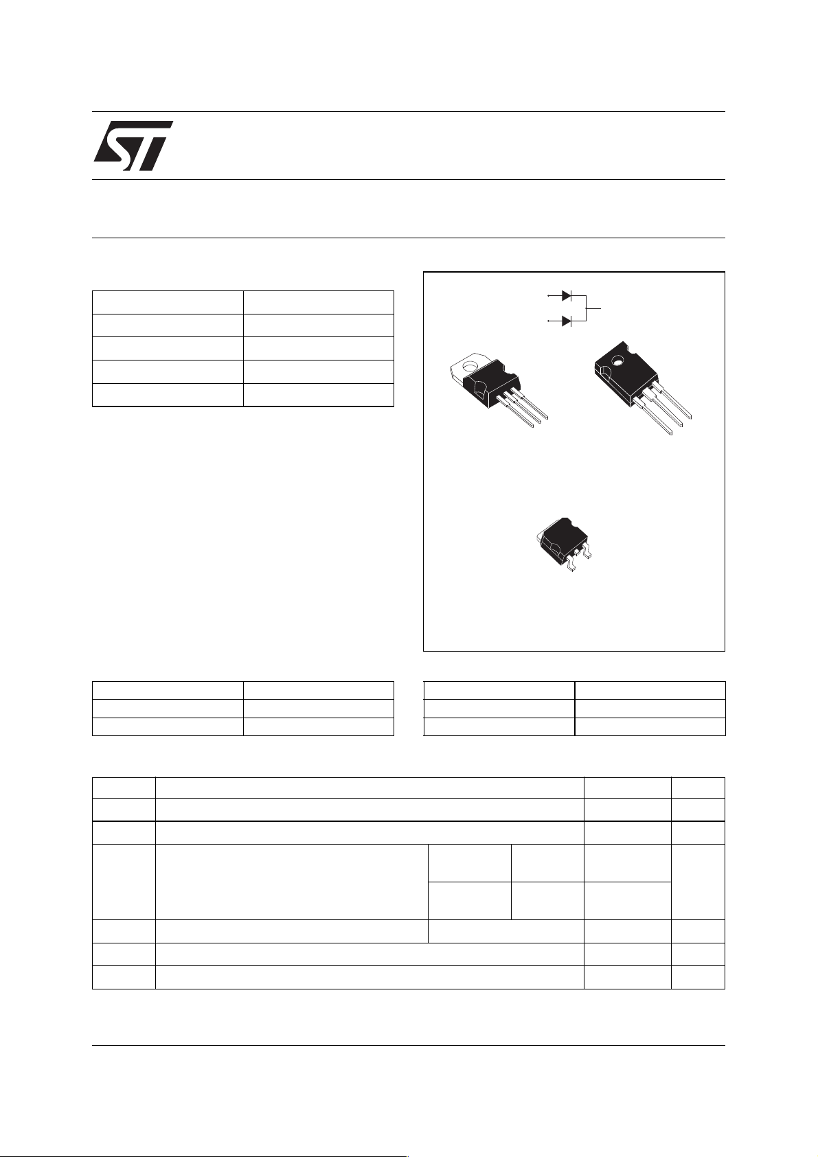
TURBO 2 ULTRAFAST HIGH VOLTAGE RECTIFIER
Table 1: Main Product Characteristics
I
F(AV)
V
RRM
T
j
VF (typ)
(max)
t
rr
Up to 2 x 20 A
600 V
175°C
0.95 V
55 ns
STTH30L06C
A1
K
A2
FEATURES AND BENEFITS
■ Ultrafast switching
■ Low reverse current
■ Low thermal resistance
■ Reduces switching & conduction losses
K
A1
TO-220AB
STTH30L06CT
K
TO-247
STTH30L06CW
A1
K
A2
DESCRIPTION
The STTH30L06, which is using ST Turbo 2 600V
technology, is specially suited for use in switching
power supplies, and industrial applications, as
rectification and discontinuous mode PFC boost
diode.
D2PA K
STTH30L06CG
A2
A1
Table 2: Order Codes
Part Number Marking
STTH30L06CT STTH30L06CT
STTH30L06CW STTH30L06CW
Part Number Marking
STTH30L06CG STTH30L06CG
STTH30L06GG-TR STTH30L06CG
Table 3: Absolute Ratings (limiting values, per diode)
Symbol Parameter Value Unit
V
RRM
I
F(RMS)
I
F(AV)
I
FSM
T
T
Repetitive peak reverse voltage 600 V
RMS forward voltage 30 A
Average forward current
δ = 0.5
Tc = 140°C
Tc = 125°C
Tc = 120°C
Tc = 110°C
Per diode
Per device
Per diode
Per device
Surge non repetitive forward current tp = 10ms sinusoidal 130 A
Storage temperature range -65 to + 175 °C
stg
Maximum operating junction temperature 175 °C
j
15
30
20
40
A2
A
September 2004 REV. 1
1/8
STTH30L06C
Table 4: Thermal Resistance
Symbol Parameter Value (max). Unit
R
th(j-c)
R
th(c)
When the diodes 1 and 2 are used simultaneously:
∆ Tj(diode 1) = P(diode 1) x R
Table 5: Static Electrical Characteristics (per diode)
Symbol Parameter Test conditions Min. Typ Max. Unit
IR * Reverse leakage current Tj = 25°C VR = V
VF ** Forward voltage drop Tj = 25°C IF = 15A 1.55 V
Pulse test: * tp = 5 ms, δ < 2%
To evaluate the conduction losses use the following equation: P = 0.94 x I
Table 6: Dynamic Characteristics (per diode)
Junction to case Per diode 1.7 °C/W
Total 1.15
Coupling 0.6 °C/W
(Per diode) + P(diode 2) x R
th(j-c)
th(c)
RRM
15 µA
Tj = 150°C 40 400
Tj = 150°C 0.95 1.2
Tj = 25°C IF = 30A 1.76
Tj = 150°C 1.15 1.45
** tp = 380 µs,
δ < 2%
F(AV)
+ 0.017 I
F2(RMS)
Symbol Parameter Test conditions Min. Typ Max. Unit
V
I
RM
t
t
Reverse recovery
rr
time
Reverse recovery
current
Forward recovery
fr
time
Forward recovery
FP
voltage
Tj = 25°C IF = 0.5A Irr = 0.25A IR =1A 55 ns
IF = 1A dIF/dt = 50 A/µs VR =30V 60 85
Tj = 125°C IF = 15A VR = 400V
8.5 12 A
dIF/dt = 100 A/µs
Tj = 25°C IF = 15A dIF/dt = 100 A/µs
VFR = 1.1 x V
Fmax
Tj = 25°C IF = 15A dIF/dt = 100 A/µs
VFR = 1.1 x V
Fmax
300 ns
3.0 V
2/8
STTH30L06C
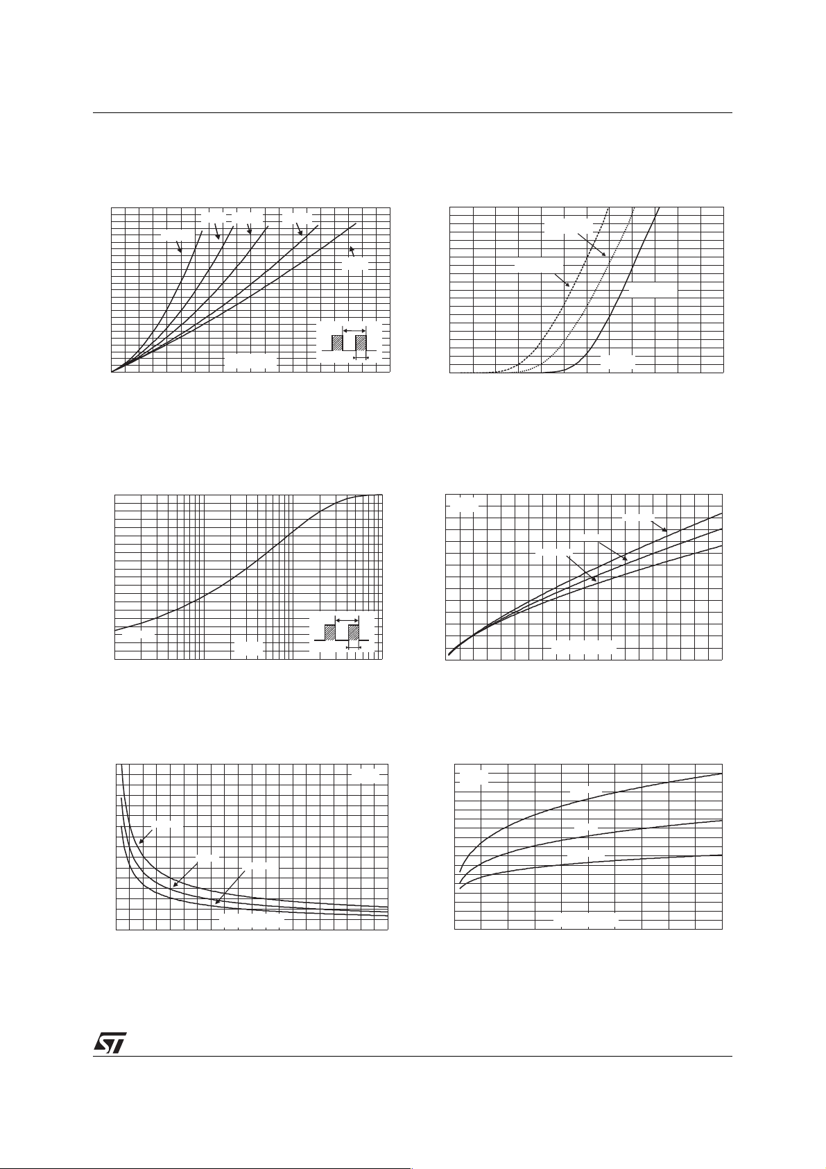
Figure 1: Conduction losses versus average
forward current (per diode)
P(W)
24
22
20
18
16
14
12
10
8
6
4
2
0
02468101214161820
δ = 0.05
δ = 0.1
δ = 0.2
I (A)
F(AV)
δ = 0.5
δ
=tp/T
δ = 1
T
tp
Figure 3: Relative variation of thermal
impedance junction to case versus pulse
duration
Z/R
th(j-c) th(j-c)
1.0
0.9
0.8
0.7
0.6
0.5
0.4
0.3
0.2
Single pulse
0.1
0.0
1.E-03 1.E-02 1.E-01 1.E+00
t (s)
p
δ
=tp/T
T
tp
Figure 2: Forward voltage drop versus forward
current (per diode)
I (A)
FM
100
T =150°C
90
80
70
60
50
40
30
20
10
0
0.0 0.5 1.0 1.5 2.0 2.5 3.0
(maximum values)
T =150°C
j
(typical values)
j
T =25°C
j
(maximum values)
V (V)
FM
Figure 4: Peak reverse recovery current versus
dIF/dt (typical values, per diode)
I (A)
RM
35
V =400V
R
T =125°C
j
30
25
20
15
10
5
0
0 50 100 150 200 250 300 350 400 450 500
I =0.5 x I
FF(AV)
I=I
dI /dt(A/µs)
F
FF(AV)
I =2 x I
FF(AV)
Figure 5: Reverse recovery time versus dIF/dt
(typical values, per diode)
t (ns)
rr
800
700
600
I =2 x I
500
400
300
200
100
0
FF(AV)
I=I
FF(AV)
0 50 100 150 200 250 300 350 400 450 500
I =0.5 x I
F F(AV)
dI /dt(A/µs)
F
V =400V
R
T =125°C
j
Figure 6: Reverse recovery charges versus
dIF/dt (typical values, per diode)
Q (nC)
rr
1800
V =400V
R
T =125°C
j
1600
1400
1200
1000
800
600
400
200
0
0 100 200 300 400 500
I =2 x I
FF(AV)
I=I
FF(AV)
I =0.5 x I
FF(AV)
dI /dt(A/µs)
F
3/8

STTH30L06C
Figure 7: Reverse recovery softness factor
versus dIF/dt (typical values, per diode)
S factor
1.6
1.4
1.2
1.0
0.8
0.6
0.4
0.2
0.0
0 50 100 150 200 250 300 350 400 450 500
dI /dt(A/µs)
F
I< 2 xI
F F(AV)
V =400V
R
T =125°C
j
Figure 9: Transient peak forward voltage
versus dIF/dt (typical values, per diode)
V (V)
FP
12
I=I
FF(AV)
11
T =125°C
j
10
9
8
7
6
5
4
3
2
1
0
0 50 100 150 200 250 300 350 400 450 500
dI /dt(A/µs)
F
Figure 8: Relative variations of dynamic
parameters versus junction temperature
1.4
1.2
1.0
0.8
0.6
0.4
0.2
0.0
25 50 75 100 125
Q
RR
t
rr
S factor
I=I
FF(AV)
V =400V
R
Reference:T =125°C
I
RM
T (°C)
j
j
Figure 10: Forward recovery time versus dIF/dt
(typical values, per diode)
t (ns)
fr
260
240
220
200
180
160
140
120
100
80
60
40
20
0
0 100 200 300 400 500
dI /dt(A/µs)
F
I=I
FF(AV)
V =1.1 x V max.
FR F
T =125°C
j
Figure 11: Junction capacitance versus
reverse voltage applied (typical values, per
diode)
C(pF)
1000
100
V (V)
10
1 10 100 1000
R
4/8
F=1MHz
V =30mV
OSC RMS
T =25°C
j
Figure 12: Thermal resistance junction to
ambient versus copper surface under tab
(epoxy FR4, eCU=35µm) (D2PAK)
R (°C/W)
th(j-a)
80
70
60
50
40
30
20
10
0
0 5 10 15 20 25 30 35 40
S (cm²)
CU

Figure 13: TO-247 Package Mechanical Data
V
V
H
L5
L
F1
V2
F(x3)
= =
F4
G
Dia.
A
L4L2
F2
L1
F3
L3
D
ME
STTH30L06C
DIMENSIONS
REF.
A 4.85 5.15 0.191 0.203
D 2.20 2.60 0.086 0.102
E 0.40 0.80 0.015 0.031
F 1.00 1.40 0.039 0.055
F1 3.00 0.118
F2 2.00 0.078
F3 2.00 2.40 0.078 0.094
F4 3.00 3.40 0.118 0.133
G 10.90 0.429
H 15.45 15.75 0.608 0.620
L 19.85 20.15 0.781 0.793
L1 3.70 4.30 0.145 0.169
L2 18.50 0.728
L3 14.20 14.80 0.559 0.582
L4 34.60 1.362
L5 5.50 0.216
M 2.00 3.00 0.078 0.118
V5° 5°
V2 60° 60°
Dia. 3.55 3.65 0.139 0.143
Millimeters Inches
Min. Typ. Max. Min. Typ. Max.
5/8

STTH30L06C
Figure 14: D2PAK Package Mechanical Data
A
L2
E
L
L3
B2
B
G
C2
D
A1
C
A2
M
* FLAT ZONE NO LESSTHAN 2mm
R
*
V2
DIMENSIONS
REF.
Millimeters Inches
Min. Max. Min. Max.
A 4.40 4.60 0.173 0.181
A1 2.49 2.69 0.098 0.106
A2 0.03 0.23 0.001 0.009
B 0.70 0.93 0.027 0.037
B2 1.14 1.70 0.045 0.067
C 0.45 0.60 0.017 0.024
C2 1.23 1.36 0.048 0.054
D 8.95 9.35 0.352 0.368
E 10.00 10.40 0.393 0.409
G 4.88 5.28 0.192 0.208
L 15.00 15.85 0.590 0.624
L2 1.27 1.40 0.050 0.055
L3 1.40 1.75 0.055 0.069
M 2.40 3.20 0.094 0.126
R 0.40 typ. 0.016 typ.
V2 0° 8° 0° 8°
Figure 15: D2PAK Foot Print Dimensions
(in millimeters)
16.90
10.30
1.30
8.90
3.70
5.08
6/8

Figure 16: TO-220AB Package Mechanical Data
A
C
L7
D
M
E
L2
F2
F1
H2
Dia
L5
L6
L9
L4
F
G1
G
STTH30L06C
DIMENSIONS
REF.
A 4.40 4.60 0.173 0.181
C 1.23 1.32 0.048 0.051
D 2.40 2.72 0.094 0.107
E 0.49 0.70 0.019 0.027
F 0.61 0.88 0.024 0.034
F1 1.14 1.70 0.044 0.066
F2 1.14 1.70 0.044 0.066
G 4.95 5.15 0.194 0.202
G1 2.40 2.70 0.094 0.106
H2 10 10.40 0.393 0.409
L2 16.4 typ. 0.645 typ.
L4 13 14 0.511 0.551
L5 2.65 2.95 0.104 0.116
L6 15.25 15.75 0.600 0.620
L7 6.20 6.60 0.244 0.259
L9 3.50 3.93 0.137 0.154
M 2.6 typ. 0.102 typ.
Diam. 3.75 3.85 0.147 0.151
Millimeters Inches
Min. Max. Min. Max.
Table 7: Ordering Information
Ordering type Marking Package Weight Base qty Delivery mode
STTH30L06CT STTH30L06CT TO-220AB 2.23 g 50 Tube
STTH30L06CG STTH30L06CG
STTH30L06CG-TR STTH30L06CG
D2PAK
D2PAK
1.48 g 50 Tube
1.48 g 1000 Tape & eel
STTH30L06CW STTH30L06CW TO-247 4.46 g 50 Tube
■ Epoxy meets UL94, V0
■ Cooling method: by conduction (C)
■ Recommended torque value: 0.8 m.N. (TO-220FPAC) / 0.55 m.N. (TO-220AB)
■ Maximum torque value: 1.0 m.N. (TO-220FPAC) / 0.70 m.N. (TO-220AB)
Table 8: Revision History
Date Revision Description of Changes
07-Sep-2004 1 First issue
7/8

STTH30L06C
Information furnished is believed to be accurate and reliable. However, STMicroelectronics assumes no responsibility for the consequences
of use of such information nor for any infringement of patents or other rights of third parties which may result from its use. No license is granted
by implication or otherwise under any patent or patent rights of STMicroelectronics. Specifications mentioned in this publication are subject
to change without notice. This publication supersedes and replaces all information previously supplied. STMicroelectronics products are not
authorized for use as critical components in life support devices or systems without express written approval of STMicroelectronics.
The ST logo is a registered trademark of STMicroelectronics.
All other names are the property of their respective owners
© 2004 STMicroelectronics - All rights reserved
Australia - Belgium - Brazil - Canada - China - Czech Republic - Finland - France - Germany - Hong Kong - India - Israel - Italy - Japan -
Malaysia - Malta - Morocco - Singapore - Spain - Sweden - Switzerland - United Kingdom - United States of America
STMicroelectronics group of companies
www.st.com
8/8
 Loading...