

Page 1
STTH212
High voltage ultrafast diode
Main product characteristics
I
F(AV)
V
V
F
t
(max)
rr
RRM
T
j
(typ)
2 A
1200 V
175°C
1.0 V
75 ns
Features and benefits
■ Low forward voltage drop
■ High reliability
■ High surge current capability
■ Soft switching for reduced EMI disturbances
■ Planar technology
Description
The STTH212, which is using ST ultrafast high
voltage planar technology, is specially suited for
free-wheeling, clamping, snubbering,
demagnetization in power supplies and other
power switching applications.
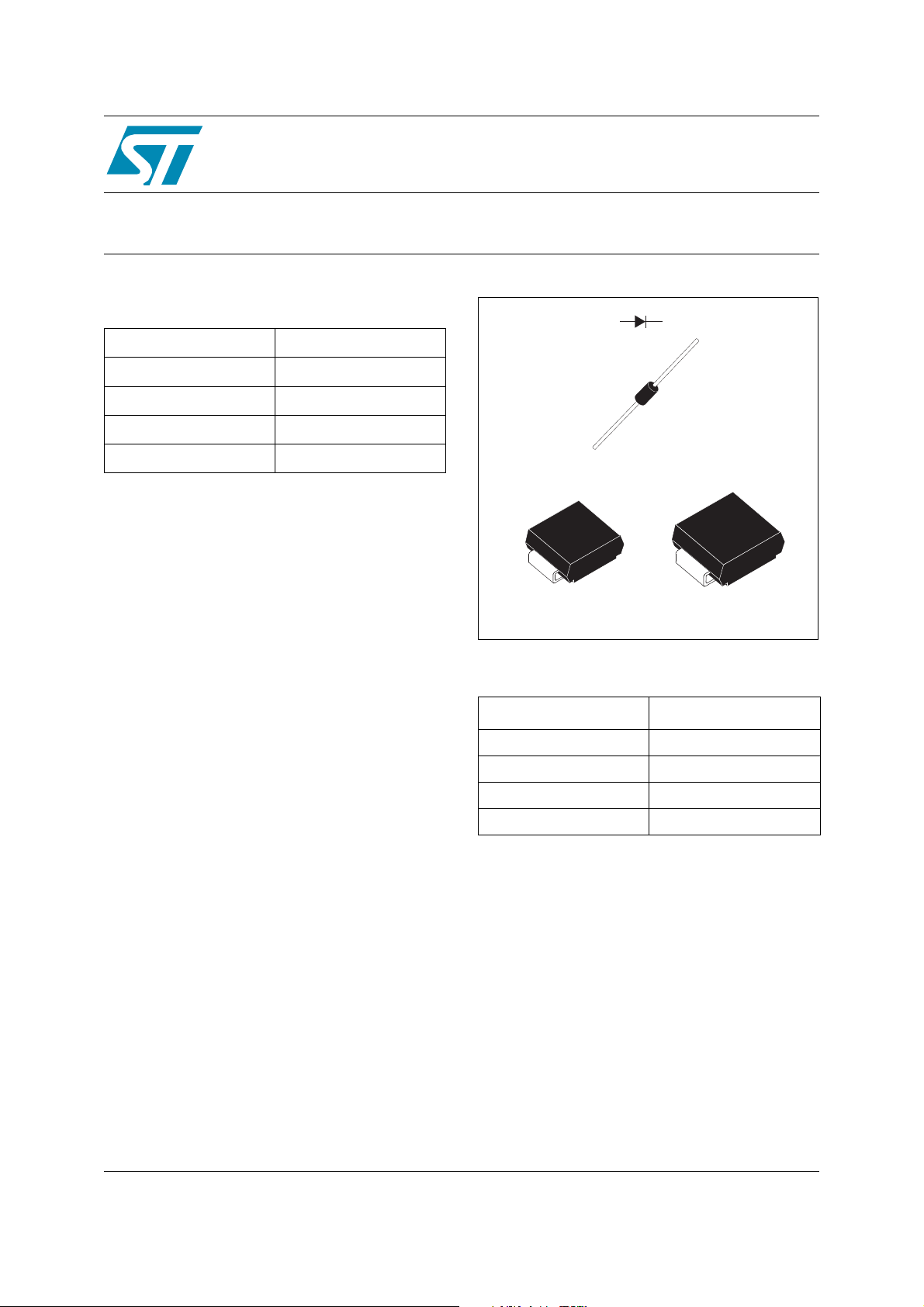
Housed in axial, SMB, and SMC packages, this
diode will reduce the losses in high switching
freqency operations.
DO-201AD
STTH212
SMB
STTH212U
Order codes
Part Number Marking
STTH212 STTH212
STTH212RL STTH212
STTH212U U22
STTH212S S12
KA
SMC
STTH212S
Rev 1
June 2005 1/9
www.st.com
9
Page 2
1 Electrical characteristics STTH212
1 Electrical characteristics
Table 1. Absolute Ratings (limiting values)
Symbol Parameter Value Unit
V
RRM
V
(RMS)
I
F(AV)
I
F(RMS)
I
FSM
T
Repetitive peak reverse voltage 1200 V
RMS voltage 850 V
= 105°C
DO-201AD
Average forward current
δ = 0.5
SMC
T
l
= 90°C
T
l
Tl = 105°C
RMS forward current DO-201AD, SMB, SMC 10 A
Forward surge current tp = 8.3ms
Storage temperature range -50 to + 175 °C
stg
T
Maximum operating junction temperature 175 °C
j
DO-201AD, SMB, SMC 40 A
2ASMB
Table 2. Thermal parameters
Symbol Parameter Value Unit
L = 10 mm DO-201AD 20
R
th(j-l)
Junction to lead
SMC 20
R
th(j-a)
Junction to ambient L = 10 mm DO-201AD 75 °C/W
Table 3. Static Electrical Characteristics
°C/WSMB 25
Symbol Parameter Test conditions Min. Typ Max. Unit
= 25°C
T
I
Reverse leakage current
R
j
= 125°C
T
j
= V
V
R
RRM
Tj = 25°C
V
Forward voltage drop
F
= 125°C
T
j
T
= 150°C
j
I
F
= 2A
To evaluate the conduction losses use the following equation: P = 1.26 x I
1.07 1.50
1.0 -
F(AV)
10
100
1.75
+ 0.12 I
F2(RMS)
2/9
µA
V
Page 3
STTH212 1 Electrical characteristics
Table 4. Dynamic Electrical Characteristics
Symbol Parameter Test conditions Min. Typ Max. Unit
t
Reverse recovery
rr
time
Forward recovery
t
fr
time
V
Forward recovery
FP
voltage
Tj = 25°C IF = 1A dIF/dt = -100 A/µs VR =30V
I
= 2A dIF/dt = 50 A/µs
Tj = 25°C
F
VFR = 1.1 x V
Fmax
75 ns
500 ns
30 V
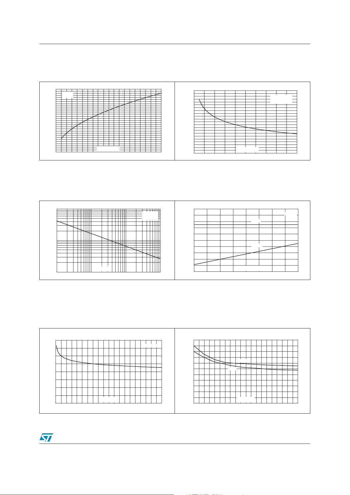
Figure 1. Conduction losses versus average
forward current
P(W)
4.0
3.5
3.0
2.5
2.0
1.5
1.0
0.5
0.0
0.00 0.25 0.50 0.75 1.00 1.25 1.50 1.75 2.00 2.25 2.50
δ = 0.05
δ = 0.1
I (A)
F(AV)
δ = 0.2
δ = 0.5
δ
=tp/T
δ = 1
T
tp
Figure 3. Relative variation of thermal
impedance junction to ambient
versus pulse duration (Epoxy
printed circuit board FR4,
L
Z
th(j-a)/Rth(j-a)
1.0
DO-201AD
0.9
=10mm
L
leads
0.8
0.7
0.6
0.5
0.4
0.3
0.2
0.1
0.0
1.E-01 1.E+00 1.E+01 1.E+02 1.E+03
Leads
= 10mm)
tp(s)
Figure 2. Forward voltage drop versus
forward current
I (A)
FM
50
45
40
35
30
25
20
15
10
5
0
0.0 0.5 1.0 1.5 2.0 2.5 3.0 3.5 4.0 4.5
T=125°C
j
(typical values)
T=125°C
j
(maximum values)
V (V)
FM
T=25°C
j
(maximum values)
Figure 4. Relative variation of thermal
impedance junction to ambient
versus pulse duration (Epoxy
printed circuit board FR4,
S
=1cm2)
CU
Z
th(j-a)/Rth(j-a)
1.0
SMB
0.9
S
=1cm²
Cu
0.8
0.7
0.6
0.5
0.4
0.3
0.2
0.1
0.0
1.E-01 1.E+00 1.E+01 1.E+02 1.E+03
tp(s)
3/9
Page 4
1 Electrical characteristics STTH212
Figure 5. Relative variation of thermal
impedance junction to ambient
versus pulse duration (Epoxy
printed circuit board FR4,
S
=1cm2)
CU
Z
th(j-a)/Rth(j-a)
1.0
SMC
0.9
=1cm²
S
Cu
0.8
0.7
0.6
0.5
0.4
0.3
0.2
0.1
0.0
1.E-01 1.E+00 1.E+01 1.E+02 1.E+03
tp(s)
Figure 7. Reverse recovery time versus dI
(typical values)
trr(ns)
900
800
700
600
500
IF=2 x I
F(AV)
F(AV)
IF=I
F(AV)IF=IF(AV)
dl /dt(A/µs)
F
400
300
200
IF=0.5 x I
100
0
0 50 100 150 200 250 300 350 400 450 500
VR=600V
Tj=125°C
Figure 6. Reverse recovery current versus
/dt (typical values)
dI
F
I (A)
RM
11
VR=600V
10
T
=125°C
j
9
8
7
6
5
4
3
2
1
0
0 20 40 60 80 100 120 140 160 180 200
/dt
Figure 8. Reverse recovery charges versus
F
Qrr(nC)
1400
VR=600V
T
1200
1000
800
600
400
200
0
0 50 100 150 200 250 300 350 400 450 500
IF=0.5 xI
IF=0.5 xI
dI
/dt (typical values)
F
=125°C
j
IF=I
)
)
F(AV
F(AV
IF=2 x I
F(AV)
IF=I
F(AV)
IF=0.5 x I
dl /dt(A/µs)
F
IF=2 x I
=2 x I
F(AV)IF
F(AV)
F(AV)IF=IF(AV)
dl /dt(A/µs)
F
F(AV)
Figure 9. Softness factor versus dI
F
/dt
(typical values)
S
FACTOR
6.0
IF=I
5.5
5.0
4.5
4.0
3.5
3.0
2.5
2.0
1.5
1.0
0.5
0.0
4/9
F(AV)
VR=600V
T
=125°C
j
dl /dt(A/µs)
F
0 25 50 75 100 125 150 175 200 225 250
Figure 10. Relative variations of dynamic
parameters versus junction
temperature
1.0
0.9
0.8
0.7
0.6
0.5
0.4
0.3
0.2
0.1
0.0
S
FAC TOR
I
RM
Q
RR
IF=I
F(AV)
Tj(°C)
25 50 75 100 125
VR=600V
Reference:T
=125°C
j
Page 5
STTH212 1 Electrical characteristics
Figure 11. Transient peak forward voltage
versus dI
V (V)
FP
30
28
IF=I
F(AV)
Tj=125°C
26
24
22
20
18
16
14
12
10
8
6
4
2
0
0 102030405060708090100
/dt (typical values)
F
dl /dt(A/µs)
F
Figure 13. Junction capacitance versus
reverse voltage applied (typical
values)
C(pF)
100
10
V (V)
1
1 10 100 1000
R
V
F=1MHz
osc
Tj=25°C
=30mV
RMS
Figure 12. Forward recovery time versus dI
(typical values)
t (ns)
FR
420
400
380
360
340
320
300
280
260
240
220
200
0 20 40 60 80 100
dl /dt(A/µs)
F
IF=I
F(AV)
VFR=1.1 x VFmax.
T
=125°C
j
Figure 14. Thermal resistance versus lead
length
R (°C/W)
th(j-a)
100
90
80
70
60
50
40
30
20
10
0
5 10152025
R
L (mm)
Leads
th(j-a)
R
th(j-l)
DO201-AD
F
/dt
Figure 15. Thermal resistance junction to
ambient versus copper surface
under each lead (Epoxy printed
circuit board FR4, e
R (°C/W)
th(j-a)
80
70
60
50
40
30
20
10
0
012345678910
S (cm )
Cu
2
= 35µm)
CU
DO-201AD
Figure 16. Thermal resistance junction to
ambient versus copper surface
under each lead (Epoxy printed
circuit board FR4, e
R (°C/W)
th(j-a)
110
100
90
80
70
60
50
40
30
20
10
0
0.0 0.5 1.0 1.5 2.0 2.5 3.0 3.5 4.0 4.5 5.0
5/9
SMC
SMB
S (cm )
Cu
2
= 35 µm)
cu
Page 6
2 Package mechanical data STTH212
2 Package mechanical data
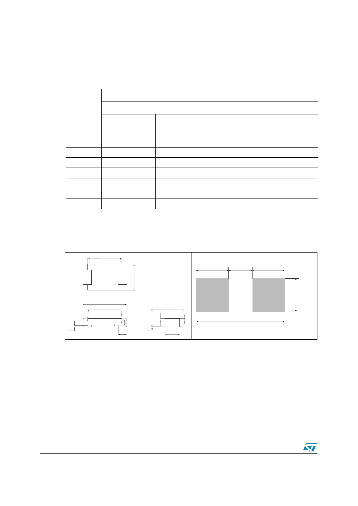
Table 5. SMB dimensions
DIMENSIONS
REF.
Millimeters Inches
Min. Max. Min. Max.
A1 1.90 2.45 0.075 0.096
A2 0.05 0.20 0.002 0.008
b 1.95 2.20 0.077 0.087
c 0.15 0.41 0.006 0.016
E 5.10 5.60 0.201 0.220
E1 4.05 4.60 0.159 0.181
D 3.30 3.95 0.130 0.156
L 0.75 1.60 0.030 0.063
Figure 17. SMB references to dimensions
table
E1
D
Figure 18. SMB footprint dimensions
(in millimetres)
2.23
1.64
2.23
E
A1
C
L
A2
b
6/9
2.30
6.10
Page 7
STTH212 2 Package mechanical data
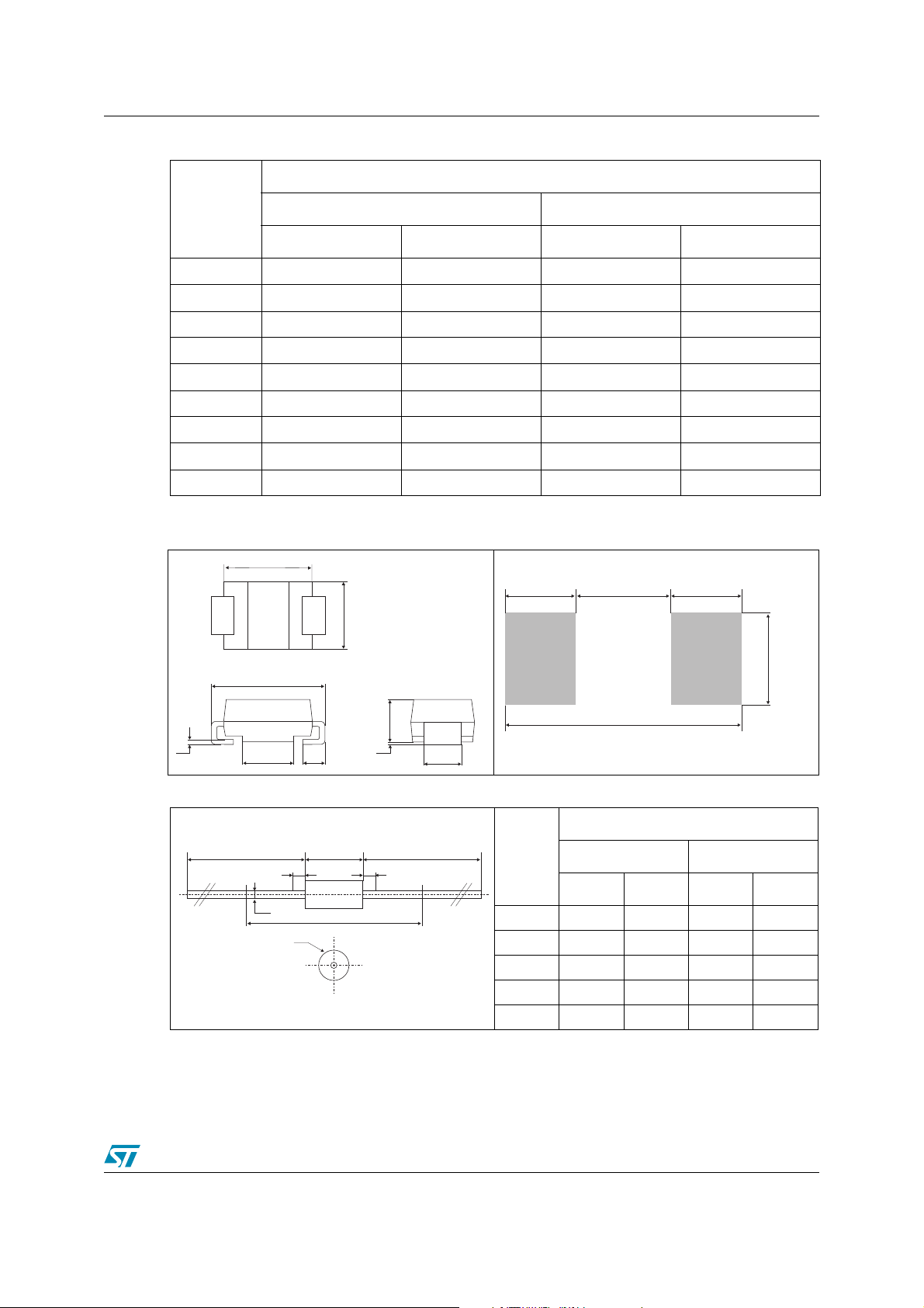
Table 6. SMC dimensions
DIMENSIONS
REF.
Millimeters Inches
Min. Max. Min. Max.
A1 1.90 2.45 0.075 0.096
A2 0.05 0.20 0.002 0.008
b 2.90 3.2 0.114 0.126
c 0.15 0.41 0.006 0.016
E 7.75 8.15 0.305 0.321
E1 6.60 7.15 0.260 0.281
E2 4.40 4.70 0.173 0.185
D 5.55 6.25 0.218 0.246
L 0.75 1.60 0.030 0.063
Figure 19. SMC references to dimensions
table
E1
D
E
Figure 20. SMC footprint dimensions
(in millimetres)
2.20
4.25
2.20
3.30
A1
C
LE2
A2
b
8.65
Table 7. DO-201AD dimensions
DIMENSIONS
BB
Note 1 Note 1
A
EE
REF.
Millimeters Inches
Min. Max. Min. Max.
ØD
ØC
Note 2
A - 9.5 - 0.37
B 25.4 - 1.00 -
C - 5.3 - 0.21
D - 1.3 - 0.051
E - 1.25 - 0.048
Note: 1 The lead diameter D is not controlled over zone E.
2 The minimum length which must stay straight between the right angles after bending is 15 mm
(0.59 inch).
7/9
Page 8
3 Ordering information STTH212
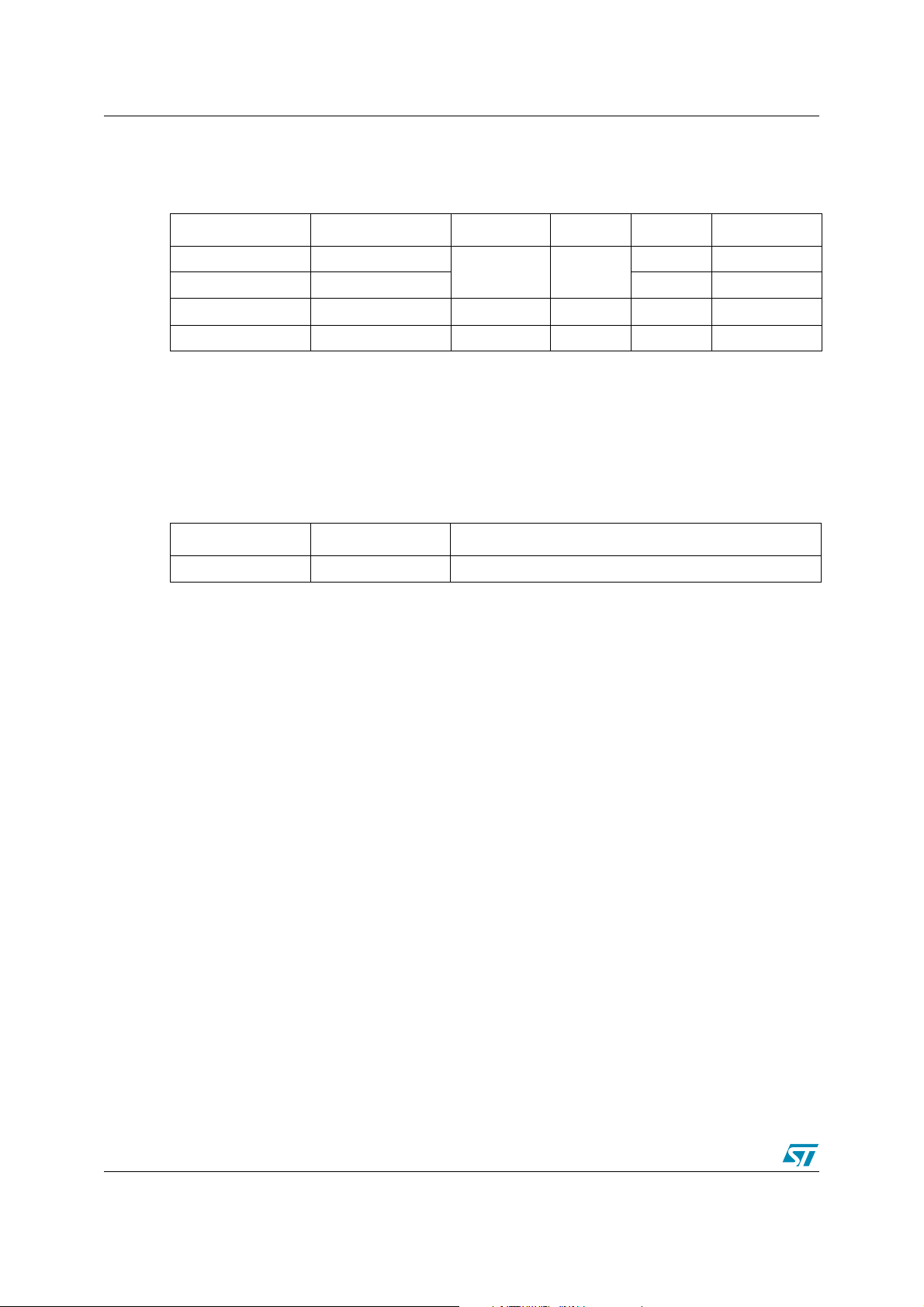
3 Ordering information
Part Number Marking Package Weight Base qty Delivery mode
STTH212 STTH212
STTH212RL STTH212 1900 Tape & reel
STTH212U U22 SMB 0.11 g 2500 Tape & reel
STTH212S S12 SMC 0.243 g 2500 Tape & reel
4 Revision history
Date Revision Description of Changes
28-Jun-2005 1 First issue.
DO-201AD 1.12 g
600 Ammopack
8/9
Page 9

STTH212 4 Revision history
Information furnished is believed to be accurate and reliable. However, STMicroelectronics assumes no responsibility for the consequences
of use of such information nor for any infringement of patents or other rights of third parties which may result from its use. No license is granted
by implication or otherwise under any patent or patent rights of STMicroelectronics. Specifications mentioned in this publication are subject
to change without notice. This publication supersedes and replaces all information previously supplied. STMicroelectronics products are not
authorized for use as critical components in life support devices or systems without express written approval of STMicroelectronics.
The ST logo is a registered trademark of STMicroelectronics.
All other names are the property of their respective owners
© 2005 STMicroelectronics - All rights reserved
STMicroelectronics group of companies
Australia - Belgium - Brazil - Canada - China - Czech Republic - Finland - France - Germany - Hong Kong - India - Israel - Italy - Japan -
Malaysia - Malta - Morocco - Singapore - Spain - Sweden - Switzerland - United Kingdom - United States of America
www.st.com
9/9
 Loading...