


HCD-FX200
Table of contents
 Loading...
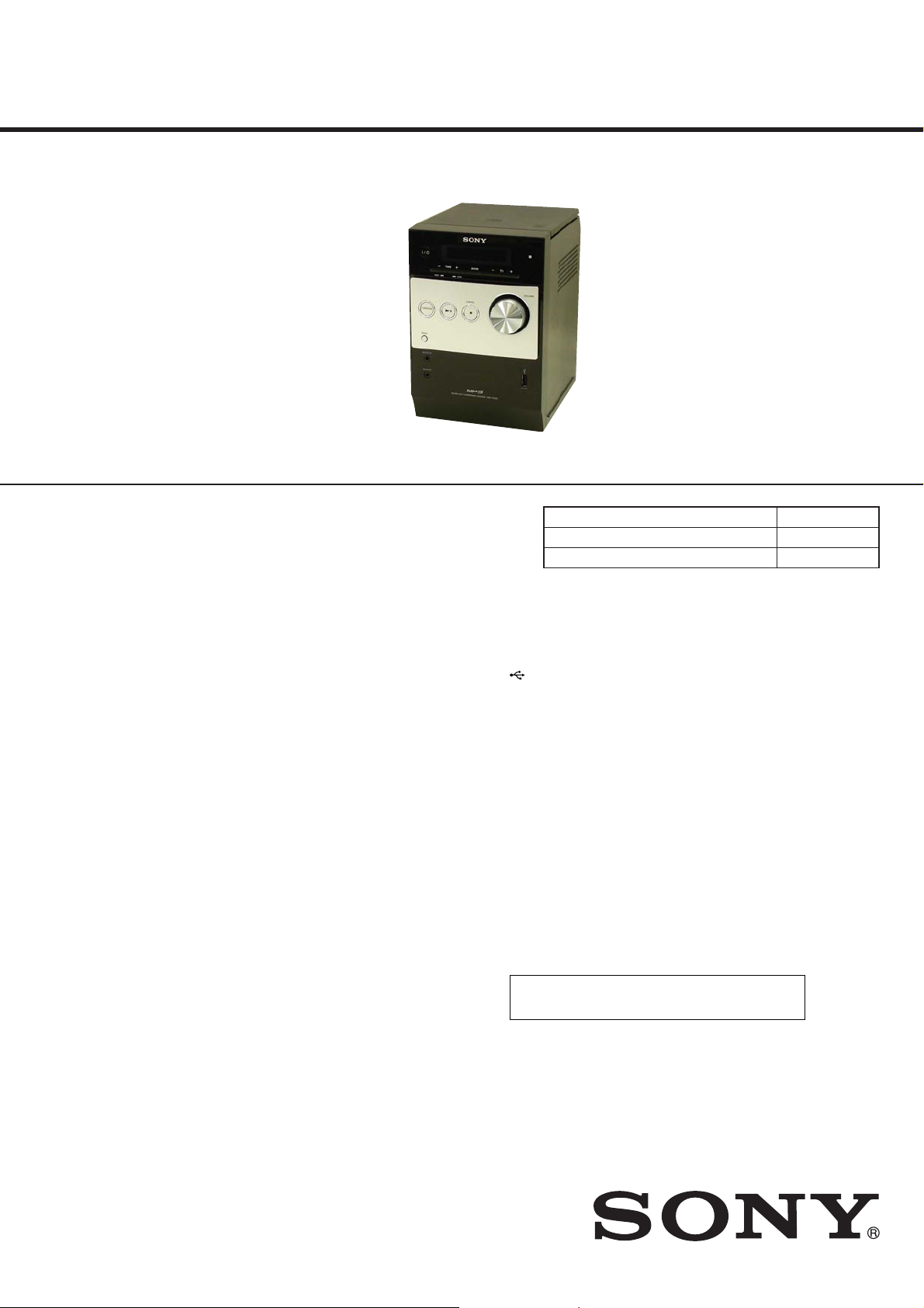
SERVICE MANUAL
Sony Corporation
Audio&Video Business Group
Published by Sony Techno Create Corporation
HCD-FX200/FX205
SPECIFICATIONS
COMPACT DISC RECEIVER
9-889-800-02
2010D05-1
©
2010.04
AEP Model
HCD-FX200/FX205
E Model
Australian Model
HCD-FX200
Ver. 1.1 2010.04
• HCD-FX200 is the amplifi er, CD player, tuner
and USB section in CMT-FX200.
• HCD-FX205 is the amplifi er, CD player, tuner
and USB section in CMT-FX205. Photo: HCD-FX200
Model Name Using Similar Mechanism
NEW
Base Unit Name
BU-D1BD73U
Optical Pick-up Block Name
DA11MMVGP
MPEG Layer-3 audio coding technology and patents
licensed from Fraunhofer IIS and omson.
All other trademarks and registered trademarks are of
their respective holders. In this manual,
TM
and
®
marks
are not specied.
Amplier section
European and Russian models:
DIN power output (rated): 4 watts + 4 watts (4 ohms at 1 kHz, DIN)
Continuous RMS power output (reference): 5 watts + 5 watts (4 ohms at
1 kHz, 10% THD)
Music power output (reference): 9 watts + 9 watts
Other models:
DIN power output (rated): 4 watts + 4 watts (4 ohms at 1 kHz, DIN)
Continuous RMS power output (reference): 5 watts + 5 watts (4 ohms at
1 kHz, 10% THD)
Input
AUDIO IN (stereo mini jack): Sensitivity 550 mV, impedance 50 kilohms
Outputs
PHONES (stereo mini jack): Accepts headphones with an impedance of
8 ohms or more
SPEAKERS: Accepts impedance of 4 ohms
CD player section
System: Compact disc and digital audio system
Laser Diode Properties
Emission Duration: Continuous
Laser Output*: Less than 44.6μW
* is output is the value measurement at a distance of 200mm from the
objective lens surface on the Optical Pick-up Block with 7mm aperture.
Frequency response: 20 Hz – 20 kHz
Signal-to-noise ratio: More than 90 dB
Dynamic range: More than 90 dB
Tuner section
FM stereo, FM/AM superheterodyne tuner
FM tuner section:
Tuning range
87.5 MHz – 108.0 MHz (50 kHz step)
Antenna: FM lead antenna
Intermediate frequency: 225 kHz
AM tuner section:
Tuning range
Models for Europe, Russia, Saudi Arabia:
531 kHz – 1,602 kHz (9 kHz step)
Australian model:
531 kHz – 1,710 kHz (9 kHz step)
530 kHz – 1,710 kHz (10 kHz step)
Latin American models:
530 kHz – 1,710 kHz (10 kHz step)
531 kHz – 1,710 kHz (9 kHz step)
Other models:
531 kHz – 1,602 kHz (9 kHz step)
530 kHz – 1,610 kHz (10 kHz step)
Antenna: AM loop antenna
Intermediate frequency: 53 kHz
USB section
Supported bit rate:
MP3 (MPEG 1 Audio Layer-3): 32 kbps – 320 kbps, VBR
Sampling frequencies:
MP3 (MPEG 1 Audio Layer-3): 32/44.1/48 kHz
(USB) port: Type A, maximum current 500 mA
General
Power requirements:
European and Russian models: AC 230 V, 50/60 Hz
Australian model: AC 230 V – 240 V, 50/60 Hz
Latin American models (except for Brazilian, Mexican and Argentine
models): AC 110 V – 120 V or 220 V – 240 V, 50/60 Hz, adjustable with
voltage selector
Argentine model: AC 220 V, 50/60 Hz
Models for Middle and Near East: AC 110 V – 120 V or 220 V – 240V,
50/60 Hz, adjustable with voltage selector
Korean model: AC 220 V, 60 Hz
Taiwan model: AC 120 V, 50/60 Hz
Other models: AC 220 V – 240 V, 50/60 Hz
Power consumption:
European and Russian models: 28 watts
Latin American models (except for Mexican and Argentine models):
28 watts
Models for Middle and Near East: 28 watts
Other models: 25 watts
Dimensions (W/H/D) (excl. speakers):
Approx. 158 mm × 240 mm × 225.5 mm
Mass (excl. speakers): Approx. 2.1 kg
Design and specications are subject to change without notice.
ai model: AC 220 V, 60 Hz
sStandby power consumption: 0.5 W
wiring boards.
sHalogenated ame retardants are not used in the certain printed
HCD-FX200/FX205
2
TABLE OF CONTENTS
NOTES ON CHIP COMPONENT REPLACEMENT
• Never reuse a disconnected chip component.
• Notice that the minus side of a tantalum capacitor may be dam-
aged by heat.
FLEXIBLE CIRCUIT BOARD REPAIRING
• Keep the temperature of soldering iron around 270 °C during
repairing.
• Do not touch the soldering iron on the same conductor of the
circuit board (within 3 times).
• Be careful not to apply force on the conductor when soldering
or unsoldering.
SAFETY-RELATED COMPONENT WARNING!
COMPONENTS IDENTIFIED BY MARK 0 OR DOTTED LINE
WITH MARK 0 ON THE SCHEMATIC DIAGRAMS AND IN
THE PARTS LIST ARE CRITICAL TO SAFE OPERATION.
REPLACE THESE COMPONENTS WITH SONY PARTS
WHOSE PART NUMBERS APPEAR AS SHOWN IN THIS
MANUAL OR IN SUPPLEMENTS PUBLISHED BY SONY.
CAUTION
Use of controls or adjustments or performance of procedures
other than those specifi ed herein may result in hazardous radia-
tion exposure.
This appliance is classifi ed as
a CLASS 1 LASER product.
This marking is located on the
rear exterior.
1. SERVICING NOTES ............................................. 3
2. DISASSEMBLY
2-1. Disassembly Flow .......................................................... 5
2-2. Panel (Rear) Block ......................................................... 5
2-3. Top Panel Block ............................................................. 6
2-4. Front Panel Block ........................................................... 6
2-5. Knob (VOL) .................................................................... 7
2-6. MAIN Board ................................................................... 7
2-7. Base Unit (BU-D1BD73U) ............................................ 8
2-8. Optical Pick-up Block (DA11MMVGP) ........................ 8
3. TEST MODE ............................................................ 9
4. ELECTRICAL CHECK ......................................... 10
5. DIAGRAMS
5-1. Block Diagram - CD, TUNER, USB Section - ............... 11
5-2. Block Diagram
- OUTPUT, PANEL, POWER SUPPLY Section - ......... 12
5-3. Printed Wiring Board - BD73U Board - ........................ 14
5-4. Schematic Diagram - BD73U Board - ........................... 15
5-5. Printed Wiring Board - USB Board - .............................. 16
5-6. Schematic Diagram - USB Board - ................................. 17
5-7. Schematic Diagram - MAIN Section (1/2) - ................... 18
5-8. Schematic Diagram - MAIN Section (2/2) - ................... 19
5-9. Printed Wiring Boards - MAIN Section - ....................... 20
5-10. Printed Wiring Board - PANEL Board - ......................... 21
5-11. Schematic Diagram - PANEL Board (1/2) - ................... 22
5-12. Schematic Diagram - PANEL Board (2/2) - ................... 23
5-13. Printed Wiring Board
- PT Board (Except E2, E51 and EA models) - ............. 24
5-14. Schematic Diagram
- PT Board (Except E2, E51 and EA models) - ............. 24
5-15. Printed Wiring Board
- PT-SW Board (E2, E51 and EA models) - .................. 25
5-16. Schematic Diagram
- PT-SW Board (E2, E51 and EA models) - .................. 25
6. EXPLODED VIEWS
6-1. Overall Section .............................................................. 32
6-2. Top Panel Section ........................................................... 33
6-3. Front Panel Section ........................................................ 34
6-4. Chassis Section ............................................................... 35
7. ELECTRICAL PARTS LIST .............................. 36
Accessories are given in the last of the electrical parts list.
Ver. 1.1
• Abbreviation
E2 : 120V AC area in E model
E51 : Chilean and Peruvian models
EA : Saudi Arabia model
HCD-FX200/FX205
3
MODEL IDENTIFICATION
- Back Panel -
Part No.
Model Part No.
FX200: AEP model
4-178-691-0[]
FX200: Russian model
4-178-692-0[]
FX200: Singapore model
4-178-693-0[]
FX200: Australian model
4-178-694-0[]
FX200: Taiwan model
4-178-695-0[]
FX200: Korean model
4-178-696-0[]
FX200: Thai model
4-178-697-0[]
FX200: Argentina model
4-178-698-0[]
FX200:
120V AC area in E, Chilean
and Peruvian models
4-178-699-0[]
FX205: AEP model
4-183-336-0[]
FX205: Russian model
4-188-763-0[]
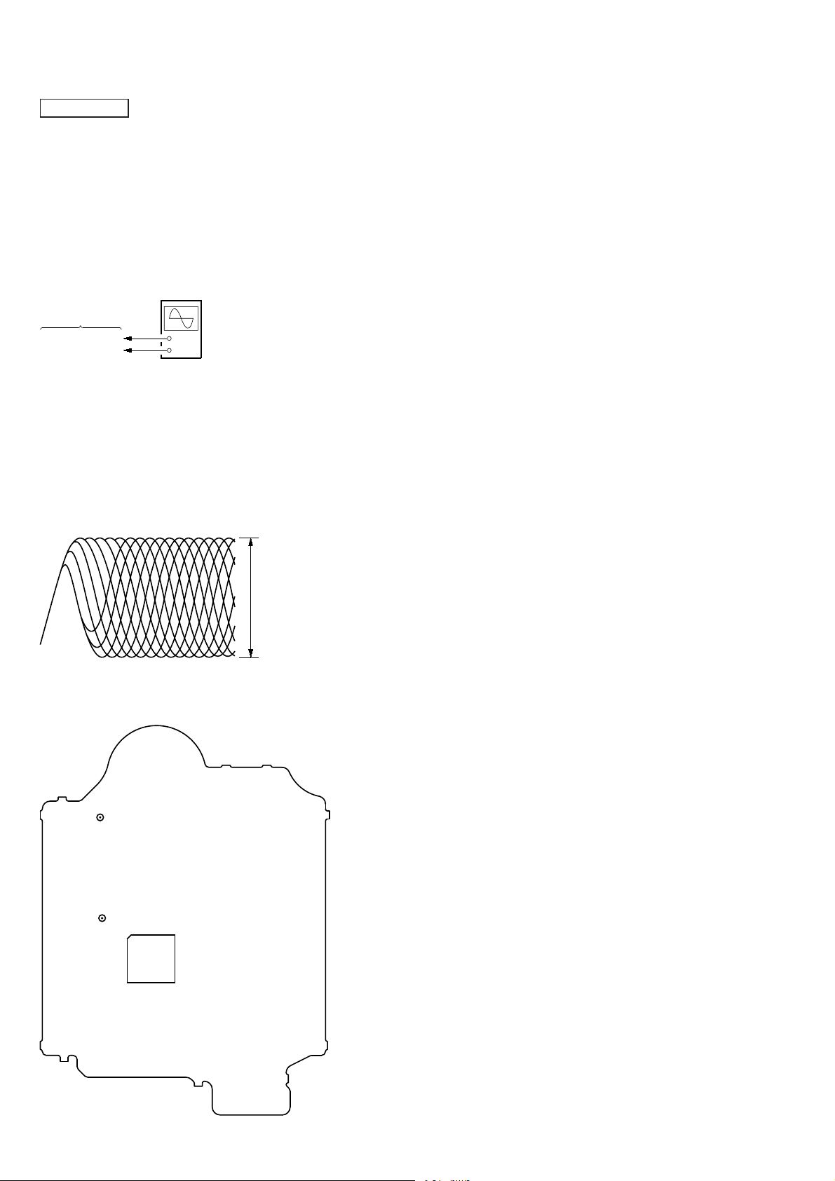
LASER DIODE AND FOCUS SEARCH OPERATION
CHECK
During normal operation of the equipment, emission of the laser
diode is prohibited unless the upper lid is closed while turning on
the SW880. (push switch type)
The following checking method for the laser diode is operable.
• Method
Emission of the laser diode is visually checked.
1. Open the upper lid.
2. Push the SW880 as shown in Fig.1.
Note: Do not push the detection lever strongly, or it may be bent or
damaged.
3. Check the object lens for confi rming normal emission of the
laser diode. If not emitting, there is a trouble in the automatic
power control circuit or the optical pick-up.
In this operation, the object lens will move up and down 2
times along with inward motion for the focus search.
SW880
Fig. 1. Method to push the SW880
SECTION 1
SERVICING NOTES
UNLEADED SOLDER
Boards requiring use of unleaded solder are printed with the lead-
free mark (LF) indicating the solder contains no lead.
(Caution: Some printed circuit boards may not come printed with
the lead free mark due to their particular size)
: LEAD FREE MARK
Unleaded solder has the following characteristics.
• Unleaded solder melts at a temperature about 40 °C higher
than ordinary solder.
Ordinary soldering irons can be used but the iron tip has to be
applied to the solder joint for a slightly longer time.
Soldering irons using a temperature regulator should be set to
about 350 °C.
Caution: The printed pattern (copper foil) may peel away if
the heated tip is applied for too long, so be careful!
• Strong viscosity
Unleaded solder is more viscous (sticky, less prone to fl ow)
than ordinary solder so use caution not to let solder bridges
occur such as on IC pins, etc.
• Usable with ordinary solder
It is best to use only unleaded solder but unleaded solder may
also be added to ordinary solder.
NOTES ON HANDLING THE OPTICAL PICK-UP
BLOCK OR BASE UNIT
The laser diode in the optical pick-up block may suffer electro-
static break-down because of the potential difference generated by
the charged electrostatic load, etc. on clothing and the human body.
During repair, pay attention to electrostatic break-down and also
use the procedure in the printed matter which is included in the
repair parts.
The fl exible board is easily damaged and should be handled with
care.
NOTE OF REPLACING THE IC101 ON THE USB
BOARD
IC101 on the USB board cannot exchange with single.
When this part on the USB board is damaged, exchange the entire
mounted board.
NOTES ON LASER DIODE EMISSION CHECK
The laser beam on this model is concentrated so as to be focused
on the disc refl ective surface by the objective lens in the optical
pickup block. Therefore, when checking the laser diode emission,
observe from more than 30 cm away from the objective lens.
Ver. 1.1
HCD-FX200/FX205
4
CAPACITOR ELECTRICAL DISCHARGE PROCESSING
When checking the board, the electrical discharge is necessary for
the electric shock prevention.
Connect the resistors referring to the fi gure below.
• PT board (C905) (Except 120V AC area in E, Saudi Arabia,
Chilean and Peruvian models only)
• PT-SW board (C905) (120V AC area in E, Saudi Arabia, Chil-
ean and Peruvian models only)
• MAIN board (C903, C904) (All models)
Both ends of respective capacitors.
– PT Board (Conductor Side) – – PT-SW Board (Conductor Side) –
– MAIN Board (Conductor Side) –
800 :/2 W
800 :/2 W
800 :/2 W
800 :/2 W
C905
C905
C903
C904
Ver. 1.1
HCD-FX200/FX205
5
SECTION 2
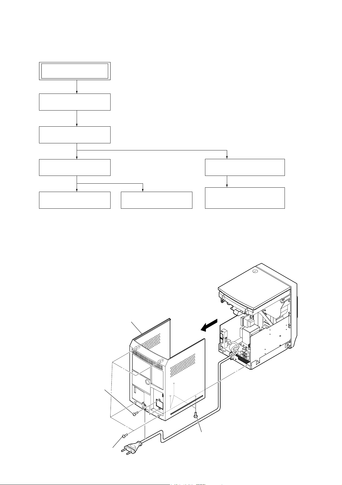
DISASSEMBLY
2-3. TOP PANEL BLOCK
(Page 6)
2-2. PANEL (REAR) BLOCK
(Page 5)
2-7. BASE UNIT (BU-D1BD73U)
(Page 8)
2-4. FRONT PANEL BLOCK
(Page 6)
2-8. OPTICAL PICK-UP BLOCK
(DA11MMVGP)
(Page 8)
2-5. KNOB (VOL)
(Page 7)
2-6. MAIN BOARD
(Page 7)
SET
3
2
two screws
(BVTP3
u
10)
4
panel (rear) block
1
three screws
(BVTP3
u
8)
2
four screws
(BVTP3
u
10)
• This set can be disassembled in the order shown below.
2-1. DISASSEMBLY FLOW
Note: Follow the disassembly procedure in the numerical order given.
2-2. PANEL (REAR) BLOCK
Note: This illustration sees the set from rear side.
HCD-FX200/FX205
6
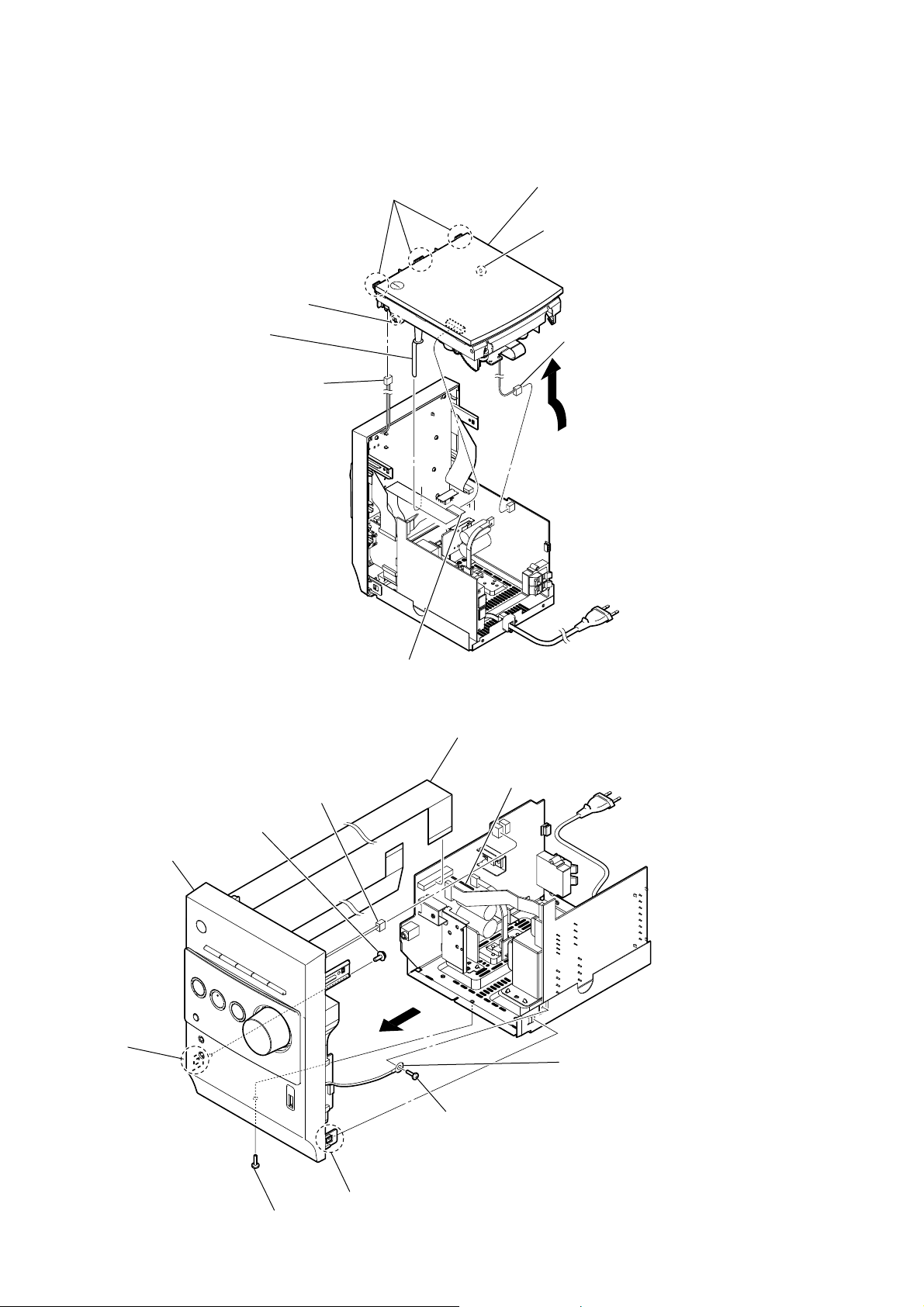
2-3. TOP PANEL BLOCK
Note: This illustration sees the set from rear side.
1
connector
(SW880)
4
connector
(CN914)
8
top panel block
5
claw
2
Extend the coating clip.
5
claw
3
flexible flat cable (19 core) (CN402)
7
three claws
6
2-4. FRONT PANEL BLOCK
0
front panel block
5
lead wire (from USB board)
8
claw
4
screw (BV3)
6
floating screw (PTPWH M2.6)
3
flexible flat cable (21 core) (CN912) (except AEP)
flexible flat cable (23 core) (CN911) (AEP)
1
connector (CN913)
2
Lift up the lead pin.
9
8
claw
7
screw
(BVTP3
u
8)
HCD-FX200/FX205
7
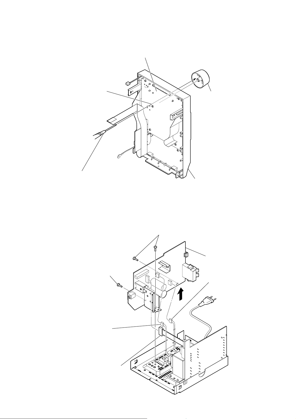
2-6. MAIN BOARD
2-5. KNOB (VOL)
Note: This illustration sees the front panel block from PANEL board side.
2
knob (VOL)
hole
1
Push the knob (VOL)
by flat-head screwdriver.
front panel block
PANEL board
3
connector
(CN904)
1
connector (CN901)
7
MAIN board
4
two screws (BV3)
6
screw
(BVTP3
u
8)
2
connector
(CN902)
5
HCD-FX200/FX205
8
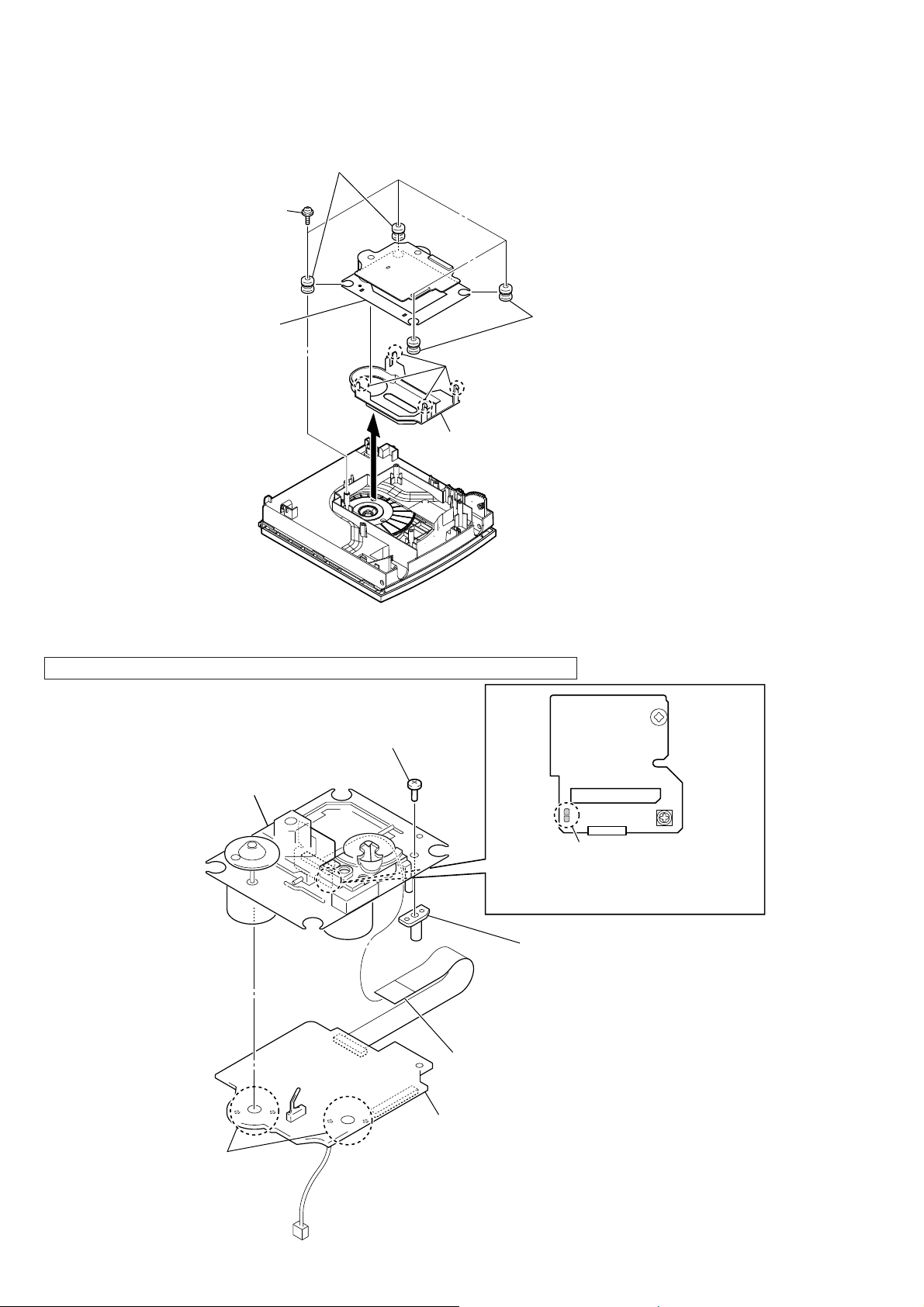
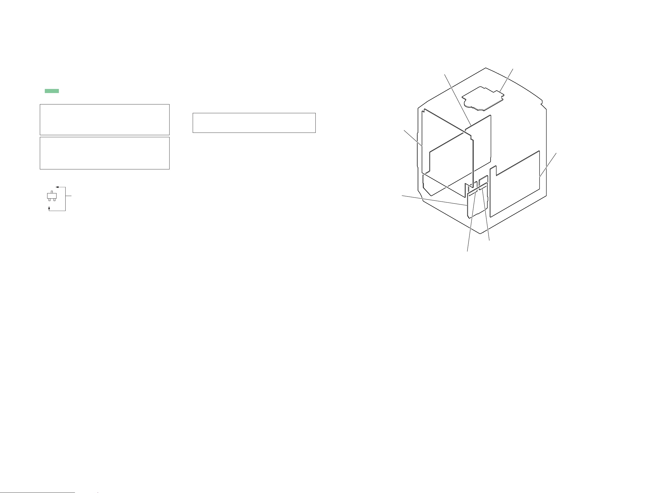
2-7. BASE UNIT (BU-D1BD73U)
Note1: This illustration sees the top panel block from base unit side.
1
four floating screws
(PTPWH M2.6)
3
two vibration proof rubbers
(red)
4
two vibration proof rubbers
(green)
6
cover (D1)
7
base unit
(BU-D1BD73U)
2
5
four claws
Note 2:
Four claws might be fixed by bond.
Please fix four claws by the bond when
you replace the cover (D1).
2-8. OPTICAL PICK-UP BLOCK (DA11MMVGP)
1
Remove four solders.
2
Solder the short-land.
4
BD73U board block
Note 2: When assembling the optical pick-up block,
remove the solder of short-land after
connecting the wire (flat type) (16 core).
7
optical pick-up block
(DA11MMVGP)
5
tapping screw (P2)
6
shaft (support)
3
wire (flat type) (16 core) (optical pick-up)
Note1: When disconnecting the wire (fl at type) (16 core) of optical pick-up block, solder the short-land.

HCD-FX200/FX205
9
SECTION 3
TEST MODE
COLD RESET
The cold reset clears all data including preset data stored in the
memory to initial conditions. Execute this mode when returning
the set to the customer.
Procedure:
1. In the standby status, press the [
?/1
] button to turn the power
on.
2. Press three buttons of [FUNCTION], [
+] and [
?/1
]simulta-
neously.
3. When “RESET” appears, the set enters standby status.
PANEL TEST MODE
Enter The Panel Test Mode
Procedure:
1. In the standby status, press the [
?/1
] button to turn the power
on.
2. Press three buttons of [ENTER], [FUNCTION] and [
?/1
] si-
multaneously.
3. When the panel test mode is activated, segments of the liquid
crystal display are all turned on.
Version Check
Procedure:
1. In the panel test mode (segments of the liquid crystal display
are all turned on), press the [ +] button.
2. On the liquid crystal display, date and version are displayed.
3. Press the [ +] button, and the USB micom version is dis-
played.
4. From this status, press the [
–] button, and the destination
and model name are displayed.
5. To release from this mode, Press three buttons of [ENTER],
[FUNCTION] and [
?/1
] simultaneously.
TUNER STEP CHANGE
(Except AEP, Russian and Saudi Arabia models only)
The AM tuning interval can be changed over 9 kHz or 10 kHz.
Procedure:
1. Press the [
?/1
] button to turn the power on.
2. Press the [FUNCTION] button to select TUNER (AM) func-
tion.
3. Press the [
?/1
] button again to turn the power off (standby).
4. After pressing the [DISPLAY] button on the remote com-
mander, while pressing the [TUNE +
M L
] button, press
the [
?/1
] button.
5. It turns power on and display “9K STEP” or “10K STEP”, and
thus the tuning interval is changed over.
CD/USB POWER MANAGE
This mode is for switch the CD/USB power supply on/off. Even if
this state pulls out AC plug, it is held.
Procedure:
1. Press the [
?/1
] button to turn the power on.
2. Press the [FUNCTION] button to select CD function.
3. Press the [
?/1
] button again to turn the power off (standby).
4. After pressing the [DISPLAY] button on the remote com-
mander, while pressing the [
x
] button, press the [
?/1
] button.
5. It turns power on and display “CD/USB”, then display “PWR
ON” or “PWR OFF”.
CD SERVICE MODE
This mode can move the SLED of the optical pick-up, and also can
turn the optical pick-up laser power on and off.
Procedure:
1. Press the [
?/1
] button to turn the power on.
2. Press the [FUNCTION] button to select CD function.
3. Press three buttons of [DSGX], [TUNE +
M L
] and [
?/1
]
simultaneously.
4. It enters the CD service mode and displays “SERVICE”.
5. To exit from this mode, press three buttons of [DSGX],
[TUNE +
M L
] and [
?/1
] simultaneously.
Key Operation:
[TUNE + M L], [– TUNE l m]:
Use these keys to move the SLED. When [TUNE + M L]
is pressed in this mode, the SLED moves to outer circumfer-
ence and the message “SLED OUT” is displayed.
When [– TUNE l m] is pressed in this mode, the SLED
moves to inner circumference and the message “SLED IN” is
displayed.
[FUNCTION]:
Use this key to turn the optical pick-up laser power on and
off. When the laser power is turned on, the message “LD ON”
is displayed. When the laser power is turned off, the message
“LD OFF” is displayed.
Ver. 1.1
HCD-FX200/FX205
10
SECTION 4
ELECTRICAL CHECK
CD SECTION
Note:
1. CD Block is basically constructed to operate without adjustment.
2. Use YEDS-18 disc (Part No. 3-702-101-01) unless otherwise indicat-
ed.
3. Use an oscilloscope with more than 10 M impedance.
4. Clean the object lens by an applicator with neutral detergent when the
signal level is low than specifi ed value with the following checks.
5. Check the focus bias check when optical pick-up block is replaced.
FOCUS BIAS CHECK
+
–
BD73U board
oscilloscope
(DC range)
CL102 (RFOUT)
CL117 (VREF)
Procedure:
1. Connect the oscilloscope to CL102 (RFOUT) and CL117
(VREF) on the BD73U board.
2. Press the [
?/1
] button to turn the power on, and press the
[FUNCTION] button to select CD function.
3. Set disc (YEDS-18) and press the [u] button to playback.
4. Confi rm that oscilloscope waveform is as shown in the fi gure
below (eye pattern).
A good eye pattern means that the diamond shape () in the
center of the waveform can be clearly distinguished.
VOLT/DIV: 200 mV
TIME/DIV: 500 ns
level:
1.1 ± 0.4 Vp-p
Checking Location:
– BD73U Board (Conductor Side) –
IC101
CL102
(RFOUT)
CL117
(VREF)
HCD-FX200/FX205
HCD-FX200/FX205
1111
SECTION 5
DIAGRAMS
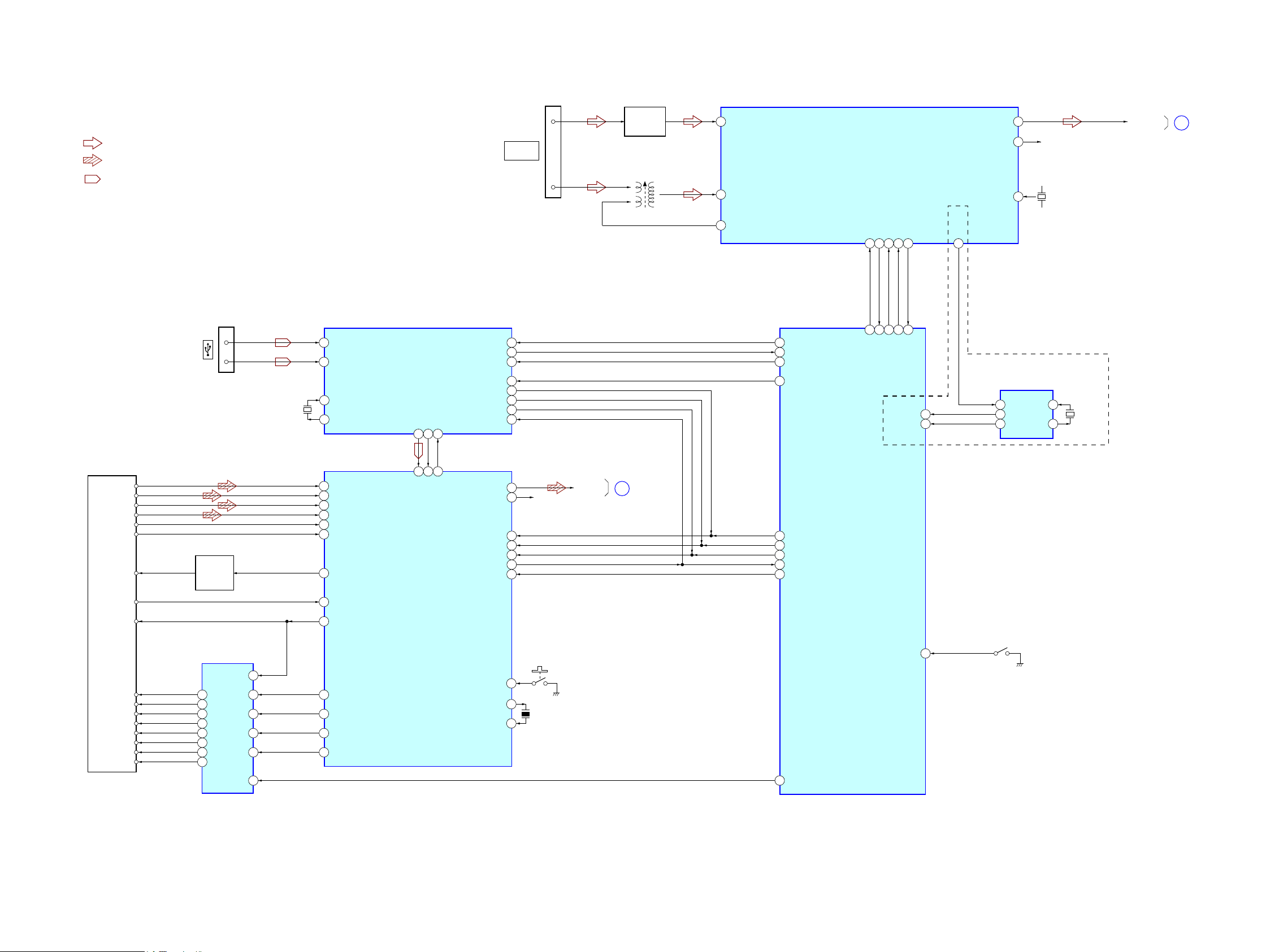
5-1. BLOCK DIAGRAM - CD, TUNER, USB Section -
B
C
D
E
A
F
SP+
SP-
LD
MD
VREF
AUTOMATIC
POWER
CONTROL
Q201
FOCUS/TRACKING COIL DRIVE,
SLED/SPINDLE MOTOR DRIVE
IC301
VO1+2
VO1-
1
IN1
3
BIAS 23
SL+
SL-
VO2-12
VO2+11
IN2’
9
T+
T-
VO3+18
VO3-
17
IN3’
20
F+
F-
VO4+26
VO4-
27
IN4’
24
MUTE 7
7BIN
6CIN
8DIN
13 EIN
5AIN
14 FIN
18 LDD
LDS
11 VREF
25 SPDO
19
24 SLDO
23 TDO
22 FDO
XOUT
XIN
X101
16.934MHz
S001
(LIMIT)
72
73
LIMIT-SW (CONT3)
32
LCHO CD/USB L76
RCHO R-CH78
CE 43
CL 44
O-CD-CE
1
O-CD-CLK
5
DO 46
DI 45
I-CD-DI4
O-CD-DO3
O-USB-TXD93
I-USB-RXD
94
O-USB-SLEEP7
O-USB-RES6
O-CD-M-MUTE
2
O-CD-RES
A
B
I-CD-SW 88
FM/AM-DET, OSC, MIX, PLL, IF AMP
IC5001
30
FM ANT
1
AM ANT
40
I-TU-DI
38
O-TU-CLK
39
O-TU-CE
37
O-TU-DO
22
_I_TUNE
X5001
32.768kHz
20
DI
19
CL
18
CE
21
DO
13
SD OUT
6
MPX OUT
3
CN5001
ANTENNA
FM/AM
1
3
2
BAND-PASS
FILTER
FL5001
SW880
(CD LID OPEN/CLOSE DETECT)
L5001
3
AM Vt
9L-OUT
10
R-OUT
16
CLK IN
R-CH
TU L/DAB L
6,*1$/3$7+
: CD PLAY
5FKLVRPLWWHGGXHWRVDPHDV/FK
: TUNER (FM/AM)
: USB
SYSTEM CONTROLLER
IC801 (1/2)
47RESB
CD-MP3 PROCESSOR
IC101
37 D-
38 D+
7CF2
6CF1
RXD
44
TXR
45
USB_SLP
47
CE
15
/RES
2
CL 11
DI
10
DO 9
USB CONTROLLER
IC101
D+
D-
35
STDATA (C2F)
34
STCK (FSEQ)
33
STREQ (DEFFCT)
31
STDATA
33
STCK
46
STREQ
100
X101
12MHz
CN105
DO
2
CL
16
FIN
4
RDS DECODER
IC5002
X5002
4.332MHz
XIN 13
XOUT
14
I-RDS-CLK
99
I-RDS-DATA 41
OPTICAL PICK-UP BLOCK
(DA11MMVGP)
(AEP)
(Page 12)
(Page 12)
Ver. 1.1
HCD-FX200/FX205
HCD-FX200/FX205
1212
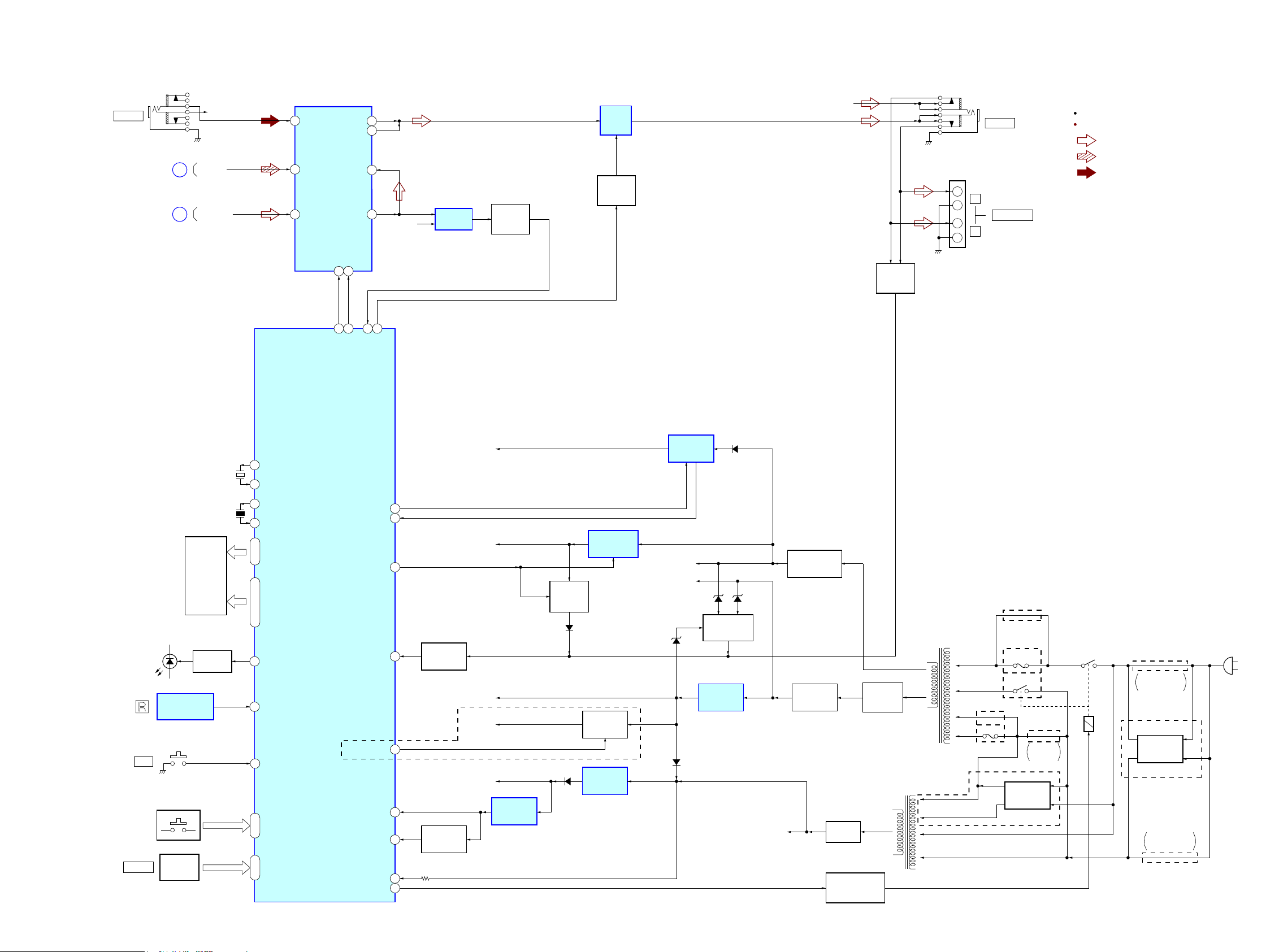
5-2. BLOCK DIAGRAM - OUTPUT, PANEL, POWER SUPPLY Section -
SYSTEM CONTROLLER
IC801 (2/2)
RESET
11
35O-POWER
42O-RDS-POWER
MAIN POWER
ON/OFF CONTROL
Q909
+9V
REGULATOR
IC901
RESET SIGNAL
GENERATOR
IC802
+4V
REGULATOR
IC970
+9V
+7V
REGULATOR
Q915, 931, 932, 940
REGULATOR
Q910, 930, 934
RDS B+
RESET
SWITCH
Q802
RDS B+
SWITCH
Q5002, 5003
SYSTEM +3.3V
D801
D907
VSTBY
RECT
D925 – 928
I_POWER_MONITOR
26
X802
15MHz
Main Clock (15MHz)
Main Clock (15MHz)
16
15
X801
32.768kHz
Sub Clock (32kHz)
Sub Clock (32kHz)
13
12
I-RMC(SIRCS)
29
REMOTE CONTROL
RECEIVER
IC860
LED DRIVE
Q860
D860
(LCD BACK LIGHT)
O-LED-LCD
87
LCD801
LIQUID
CRYSTAL
DISPLAY
ROTARY
ENCODER
S850
VOLUME
S820 – 824,
S830 – 833
(FRONT PANEL KEYS)
I-KEY1, I-KEY2
19, 20
I-VOL-ENC-A,
I-VOL-ENC-B
32, 33
COM1 – COM4
83 – 86
SEG1 – SEG32
46 – 53, 56 – 79
_I-AC-CUT
27
VM (7V)
AMP VCC
VBUS
D980
D802
+5V
REGULATOR
IC981
CD +3.3V
+3.3V
REGULATOR
IC980, Q981, 982
OVER VOLTAGE
DETECT
Q960
D910
D913
D931
PROTECT
DETECT
Q987
– 989
30I-PROTECT
8O-USB-POW
36O-CD-POW
PROTECT
SWITCH
Q801
R-CH
R-CH
J320
5 IN-L4
28
SDA
27
SCL
32
12
IN-L1
SEL L
1 IN-L2
O-AUDIO IC-DATA
23
O-AUDIO IC-CLK
24
I-LEVEL
25
O-AMP-ON
34
13VOL L
ELECTRICAL VOLUME,
INPUT SELECTOR
IC301
: TUNER (FM/AM)
: CD PLAY
SIGNAL PATH
R-ch is omitted due to same as L-ch.
: AUDIO IN
A
CD/USB L
B
TU L/DAB L
MIXER
IC310
25OUT L
24SB L
J350
R-CH
PHONES
POWER
AMP
IC350
STANDBY
SWITCH
Q902, 903
LEVEL
DETECT
Q301, 302
+
–
–
+
J351
OVER LOAD
DETECT
Q150, 250
AUDUO IN
10I-OVERCURRENT
S840
I/1
_I_WAKEUP28
$EEUHYLDWLRQ
$86 $XVWUDOLDQPRGHO
( 9$&DUHDLQ(PRGHO
( &KLOHDQDQG3HUXYLDQPRGHOV
($ 6DXGL$UDELDPRGHO
.5 .RUHDQPRGHO
RU : Russian model
63 6LQJDSRUHPRGHO
TH : Thai model
TW : Taiwan model
SPEAKER
R
L
RECT
D902, 903,
D905, 906
T002 (AEP, RU, AR, KR, TH)
T004 (E2, E51, EA, SP, TW, AUS)
SUB POWER
TRANSFORMER
T001
MAIN POWER
TRANSFORMER
LINE FILTER
LF901
(AC IN)
F001
RY002-1 (E2, E51, EA)
RY001 (Except E2, E51, EA)
(AEP, RU, KR)
(AEP, RU, SP, AR, KR, TH, AUS)
(Except TW)
(TW)
RY002-2
VOLGATE
SELECTOR
S001
(E2, E51, EA)
(E2, E51, EA, TW)
(E2, E51, EA)
Except E2,
E51, EA
F002
RDS B+
(AEP)
E2, E51, EA, SP,
TW, AR, TH, AUS
E2, E51, EA, SP,
TW, AR, TH, AUS
(Page 11)
(Page 11)
Ver. 1.1
HCD-FX200/FX205
HCD-FX200/FX205
1313
For Schematic Diagrams.
Note:
• All capacitors are in μF unless otherwise noted. (p: pF) 50
WV or less are not indicated except for electrolytics and
tantalums.
• All resistors are in Ω and 1/4 W or less unless otherwise
specifi ed.
•
f
: internal component.
• C : panel designation.
THIS NOTE IS COMMON FOR PRINTED WIRING BOARDS AND SCHEMATIC DIAGRAMS.
(In addition to this, the necessary note is printed in each block.)
For Printed Wiring Boards.
Note:
• X : parts extracted from the component side.
• Y : parts extracted from the conductor side.
• W : indicates side identifi ed with part number.
• : Pattern from the side which enables seeing.
(The other layers' patterns are not indicated.)
• Indication of transistor.
C
B
These are omitted.
E
Q
Caution:
Pattern face side:
(SIDE B)
Parts face side:
(SIDE A)
Parts on the pattern face side seen
from the pattern face are indicated.
Parts on the parts face side seen from
the parts face are indicated.
Caution:
Pattern face side:
(Conductor Side)
Parts face side:
(Component Side)
Parts on the pattern face side seen
from the pattern face are indicated.
Parts on the parts face side seen from
the parts face are indicated.
• Abbreviation
AUS : Australian model
E2 : 120V AC area in E model
E51 : Chilean and Peruvian models
EA : Saudi Arabia model
KR : Korean model
RU : Russian model
SP : Singapore model
TH : Thai model
TW : Taiwan model
• Circuit Boards Location
BD73U board
POWER-TR board
REG board
PANEL board
MAIN board
PT board (except E2, E51, EA)
PT-SW board (E2, E51, EA)
USB board
• A : B+ Line.
• Voltages and waveforms are dc with respect to ground
under no-signal (detuned) conditions.
– CD Board –
no mark
: CD PLAY
– USB Board –
no mark
: USB
– Other Boards –
no mark
: TUNER (FM)
[ ] : TUNER (AM)
( ) : CD PLAY
< > : USB
*
: Impossible to measure
• Voltages are taken with VOM (Input impedance 10 MΩ).
Voltage variations may be noted due to normal production
tolerances.
• Waveforms are taken with a oscilloscope.
Voltage variations may be noted due to normal production
tolerances.
• Circled numbers refer to waveforms.
• Signal path.
F : TUNER (FM/AM)
J : CD PLAY
d : USB
f : AUDIO IN
• Abbreviation
AUS : Australian model
E2 : 120V AC area in E model
E51 : Chilean and Peruvian models
EA : Saudi Arabia model
KR : Korean model
RU : Russian model
SP : Singapore model
TH : Thai model
TW : Taiwan model
Note: The components identifi ed by mark 0 or dotted
line with mark 0 are critical for safety.
Replace only with part number specifi ed.
• Abbreviation
E2 : 120V AC area in E model
E51 : Chilean and Peruvian models
EA : Saudi Arabia model
Ver. 1.1

HCD-FX200/FX205
HCD-FX200/FX205
1414
5-3. PRINTED WIRING BOARD - BD73U Board -
B
E
R412
R413
R417
C206
C207
C208
C209
C401
C402
C403
C404
C409
S001
C410
C413
C414
R117
R121
C301
C113
C116
C119
C124
C129
Q201
R201
R202
R203
1
1
19
116
28
78
1
22
21
15
14
30
29
R401
R402
R406
R407
R408
R409
R411
CN201
CN402
C201
C203
C205
CL101
CL102
CL103
CL104
CL105
CL106
CL107
CL108
CL109
CL110
CL111
CL112
CL113
CL114
CL115
CL116
CL117
CL118
CL119
CL120
CL121
SL301
SL302
SL303
SL304
R101
R102
R103
R104
R105
R106
R107
R108
R109
R301
R302
R303
R304
R111
R305
R112
R113
R114
R116
R118
R120
R122
R123
R124
R125
R126
C101
C102
C103
C104
C105
C106
C107
C108
C302
C303
C110
C304
C111
X101
C112
C117
C118
C120
C121
CL201
C122
CL202
C123
CL203
CL204
C125
CL205
C126
CL206
C127
CL207
C128
CL208
CL209
CL401
CL402
CL403
C130
CL210
CL404
C131
CL211
CL405
C132
CL212
CL406
C133
CL407
CL213
CL214
CL408
CL409
C136
CL411
CL412
CL413
CL414
CL415
CL416
CL417
CL418
CL419
CL420
CL421
CL422
CL423
SL201
IC101
IC301
(LIMIT)
1
20
60
6180
4021
41
A
USB
BOARD
CN102
1-880-980-
11
(11)
1-880-980-
R405
R404
11
(11)
BD73U BOARD (COMPONENT SIDE)
BD73U BOARD (CONDUCTOR SIDE)
M M
(SLED)(SPINDLE)
SP+
SP–
SL+
SL–
SP+
SP–
SL+
SL–
A
B
C
D
E
1 2 3 4 5 6 7
(VREF)
(RFOUT)
R403
C408
J
MAIN
BOARD
CN914
W101
OPTICAL PICK-UP BLOCK
(DA11MMVGP)
(Page 16)
• : Uses unleaded solder.
• See page 13 for Circuit Boards Location.
(Page 20)
Loading...