


 Loading...
HCD-BX6AV/DX6AV
SERVICE MANUAL
Ver 1.1 2001.07
HCD-BX6AV/DX6AV is the Amplifier, |
|
|
CD player, Tape player and Tuner |
Photo: HCD-BX6AV |
|
section in MHC-BX6AV/DX6AV. |
||
|
US Model
Canadian Model
AEP Model
UK Model
HCD-BX6AV
E Model
Australian Model
HCD-DX6AV
Manufactured under license from Dolby Laboratories Licensing Corporation. Additionally licensed under Canadian patent 1,037,877. “Dolby”, the double-D symbol ;and “PRO LOGIC” are trademarks of Dolby Laboratories Licensing Corporation.
|
Model Name Using Similar Mechanism |
HCD-BX2/DX2 |
|
CD |
|
|
|
CD Mechanism Type |
EXL-M7 |
||
Section |
|||
|
|
||
Optical Pick-up Name |
OPTIMA-7 |
||
|
|||
Tape deck |
Model Name Using Similar Mechanism |
HCD-RXD6AV |
|
Section |
|
|
|
Tape Transport Mechanism Type |
CWL-44-RR |
||
|
|||
|
|
|
SPECIFICATIONS
AUDIO POWER SPECIFICATIONS: (US model only)
POWER OUTPUT AND TOTAL HARMONIC DISTORTION:
with 6 ohm loads both channels driven, from 120-10,000 Hz; rates 10 watts per channel minimum RMS power, with no more than 10% total harmonic distortion from 250 milliwatts to rated output.
Amplifier section
US model Center Speaker:
Continuous RMS power output (reference) 40 watts
(6 ohms at 1 kHz, 10% THD)
Rear Speaker:
Continuous RMS power output (reference) 40 + 40 watts
(6 ohms at 1 kHz, 10% THD)
Canadian model Front Speaker:
Continuous RMS power output (reference) 60 + 60 watts
(6 ohms at 1 kHz, 10% THD)
Total harmonics distortion
Less than 0.07%
(6 ohms at 1 kHz, 30 W)
Center Speaker:
Continuous RMS power output (reference) 40 watts
(6 ohms at 1 kHz, 10% THD)
Rear Speaker:
Continuous RMS power output (reference) 40 + 40 watts
(6 ohms at 1 kHz, 10% THD)
AEP, UK models Front Speaker:
DIN power output (rated) 40 + 40 watts
(6 ohms at 1 kHz, DIN) Continuous RMS power output (reference)
50 + 50 watts
(6 ohms at 1 kHz, 10% THD)
Music power output (reference)
100 + 100 watts (6 ohms at 1 kHz, 10% THD)
Center Speaker:
DIN power output (rated) 25 watts
(6 ohms at 1 kHz, DIN) Continuous RMS power output (reference)
35 watts
(6 ohms at 1 kHz, 10% THD)
Music power output (reference) 70 watts
(6 ohms at 1 kHz, 10% THD)
Rear Speaker:
DIN power output (rated) 25 + 25 watts
(6 ohms at 1 kHz, DIN) Continuous RMS power output (reference)
35 + 35 watts
(6 ohms at 1 kHz, 10% THD)
Music power output (reference)
70 + 70 watts
(6 ohms at 1 kHz, 10% THD)
Other models:
The following measured at AC 120/240 V, 50/60 Hz
Front Speaker:
DIN power output (rated) 45 + 45 watts
(6 ohms at 1 kHz, DIN) Continuous RMS power output (reference)
60 + 60 watts
(6 ohms at 1 kHz, 10% THD)
Center Speaker:
DIN power output (rated) 30 watts
(6 ohms at 1 kHz, DIN) Continuous RMS power output (reference)
40 watts
(8 ohms at 1 kHz, 10% THD)
Rear Speaker:
DIN power output (rated) 30 + 30 watts
(6 ohms at 1 kHz, DIN)
Continuous RMS power output (reference) 40 + 40 watts
(6 ohms at 1 kHz, 10% THD)
Inputs |
|
MD/VIDEO IN: |
voltage 250/450 mV, |
(phono jacks) |
impedance 47 kilohms |
DVD INPUT: |
|
FRONT IN: |
voltage 450 mV, |
(phono jacks) |
impedance 47 kilohms |
REAR IN: |
voltage 450 mV, |
(phono jacks) |
impedance 47 kilohms |
CENTER IN: |
voltage 450 mV, |
(phono jacks) |
impedance 47 kilohms |
WOOFER IN: |
voltage 450 mV, |
(phono jacks) |
impedance 47 kilohms |
Outputs |
|
PHONES: |
accepts headphones of |
(stereo mini jack) |
8 ohms or more |
FRONT SPEAKER: |
accepts impedance of 6 to |
|
16 ohms |
REAR SPEAKER: |
accepts impedance of 6 to |
|
16 ohms |
CENTER SPEAKER: |
accepts impedance of 6 to |
|
16 ohms |
WOOFER: |
Voltage 1 V, impedance |
|
1 kilohms |
CD player section
System |
Compact disc and digital |
|
audio system |
Laser |
Semiconductor laser |
|
(λ =780nm) |
|
Emission duration: |
|
continuous |
Laser output |
Max. 44.6 W* |
|
*This output is the value |
|
measured at a distance of |
|
200 mm from the |
|
objective lens surface on |
|
the Optical Pick-up Block |
|
with 7 mm aperture. |
|
– Continued on next page – |
COMPACT DISC DECK RECEIVER
9-929-250-12 |
Sony Corporation |
2001G0500-1 |
Home Audio Company |
C 2001.7 |
Shinagawa Tec Service Manual Production Group |

Tuning range |
|
US, Canadian models: |
530 – 1,710 kHz |
|
(with the interval set at |
|
10 kHz) |
|
531 – 1,710 kHz |
|
(with the interval set at |
|
9 kHz) |
AEP, UK and Middle Eastern models: |
|
|
531 – 1,602 kHz |
|
(with the interval set at |
|
9 kHz) |
Other models: |
531 – 1,602 kHz |
|
(with the interval set at |
|
9 kHz) |
|
530 – 1,710 kHz |
|
(with the interval set at |
|
10 kHz) |
Antenna |
AM loop antenna |
Antenna terminals |
External antenna terminal |
Intermediate frequency |
450 kHz |
General
Power requirements |
|
US, Cnadian models: |
120 V AC, 60 Hz |
AEP, UK models: |
230 V AC, 50/60 Hz |
Australian model: |
220 – 240 V AC, 50/60 Hz |
Mexican model: |
120 V AC, 60 Hz |
Other models: |
110 – 120 V or 220 – 240 V AC, 50/ |
|
60 Hz |
|
Adjustable with voltage selector |
Power consumption |
|
US model: |
160 watts |
Canadian model: |
180 watts |
AEP, UK models: |
160 watts |
Other models: |
160 watts |
Dimensions (w/h/d) |
Approx. 280 x 325 x 390 mm |
Mass |
|
US model: |
Approx. 9.2 kg |
Canadian model: |
Approx. 9.2 kg |
AEP, UK models: |
Approx. 9.2 kg |
Other model: |
Approx. 9.1 kg |
Supplied accessories: |
AM loop antenna (1) |
|
FM lead antenna (1) |
|
Remote Commander (1) |
|
Speaker cords (2) |
|
Center speaker pads (4) |
Design and specifications are subject to change without notice.
SAFETY-RELATED COMPONENT WARNING!!
COMPONENTS IDENTIFIED BY MARK 0 OR DOTTED LINE WITH MARK 0 ON THE SCHEMATIC DIAGRAMS
AND IN THE PARTS LIST ARE CRITICAL TO SAFE OPERATION. REPLACE THESE COMPONENTS WITH SONY PARTS WHOSE PART NUMBERS APPEAR AS SHOWN IN THIS MANUAL OR IN SUPPLEMENTS PUBLISHED BY SONY.
ATTENTION AU COMPOSANT AYANT RAPPORT
À LA SÉCURITÉ!
LES COMPOSANTS IDENTIFIÉS PAR UNE MARQUE 0
SUR LES DIAGRAMMES SCHÉMATIQUES ET LA LISTE DES PIÈCES SONT CRITIQUES POUR LA SÉCURITÉ DE FONCTIONNEMENT. NE REMPLACER CES COMPOSANTS QUE PAR DES PIÈCES SONY DONT LES NUMÉROS SONT DONNÉS DANS CE MANUEL OU DANS LES SUPPLÉMENTS PUBLIÉS PAR SONY.
|
TABLE OF CONTENTS |
|
1. |
SERVICING NOTES ............................................... |
3 |
2. |
GENERAL |
|
|
Location of Controls ....................................................... |
4 |
|
Setting the Time .............................................................. |
5 |
3. |
DISASSEMBLY ......................................................... |
6 |
4.DIAGRAMS
4-1. Note for Printed Wiring Boards and |
|
|||
|
Schematic Diagrams |
....................................................... |
|
11 |
4-2. |
Schematic Diagram |
– CD Section (1/4) – ..................... |
12 |
|
4-3. |
Schematic Diagram |
– CD Section (2/4) – ..................... |
13 |
|
4-4. |
Schematic Diagram |
– CD Section (3/4) – ..................... |
14 |
|
4-5. |
Schematic Diagram |
– CD Section (4/4) – ..................... |
15 |
|
4-6. |
Printed Wiring Boards |
– CD Section – ......................... |
16 |
|
4-7. |
Printed Wiring Boards |
– MAIN Section – .................... |
17 |
|
4-8. |
Schematic Diagram – MAIN Section (1/4) – ................ |
18 |
||
4-9. |
Schematic Diagram – MAIN Section (2/4) – ................ |
19 |
||
4-10. |
Schematic Diagram – MAIN Section (3/4) – ................ |
20 |
||
4-11. Schematic Diagram – MAIN Section (4/4) – ................ |
21 |
|||
4-12. |
Printed Wiring Boards – PANEL Section – .................. |
22 |
||
4-13. Schematic Diagram – PANEL Section – ....................... |
23 |
|||
4-14. Printed Wiring Boards |
|
|
||
|
– AMP/POWER SUPPLY Section – ............................. |
24 |
||
4-15. |
Schematic Diagram – FRONT AMP Section – ............ |
25 |
||
4-16. |
Schematic Diagram |
|
|
|
|
– CENTER/REAR AMP Section – ................................. |
26 |
||
4-17. |
Schematic Diagram – POWER SUPPLY Section – ...... |
27 |
||
5. |
EXPLODED VIEWS ................................................ |
33 |
||
6. |
ELECTRICAL PARTS LIST ............................... |
39 |
||
Notes on chip component replacement
•Never reuse a disconnected chip component.
•Notice that the minus side of a tantalum capacitor may be damaged by heat.
Flexible Circuit Board Repairing
•Keep the temperature of the soldering iron around 270 ˚C during repairing.
•Do not touch the soldering iron on the same conductor of the circuit board (within 3 times).
•Be careful not to apply force on the conductor when soldering or unsoldering.
CAUTION
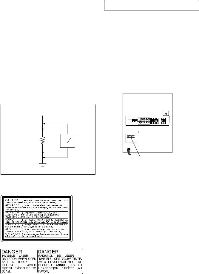
Use of controls or adjustments or performance of procedures other than those specified herein may result in hazardous radiation exposure.
This appliance is classified as a CLASS 1 LASER product. The CLASS 1 LASER PRODUCT MARKING is located on the rear exterior.
2
SAFETY CHECK-OUT
After correcting the original service problem, perform the following safety check before releasing the set to the customer:
Check the antenna terminals, metal trim, “metallized” knobs, screws, and all other exposed metal parts for AC leakage.
Check leakage as described below.
LEAKAGE TEST
The AC leakage from any exposed metal part to earth ground and from all exposed metal parts to any exposed metal part having a return to chassis, must not exceed 0.5 mA (500 microamperes.). Leakage current can be measured by any one of three methods.
1.A commercial leakage tester, such as the Simpson 229 or RCA WT-540A. Follow the manufacturers’ instructions to use these instruments.
2.A battery-operated AC milliammeter. The Data Precision 245 digital multimeter is suitable for this job.
3.Measuring the voltage drop across a resistor by means of a VOM or battery-operated AC voltmeter. The “limit” indication is 0.75 V, so analog meters must have an accurate lowvoltage scale. The Simpson 250 and Sanwa SH-63Trd are examples of a passive VOM that is suitable. Nearly all battery operated digital multimeters that have a 2 V AC range are suitable. (See Fig. A)
To Exposed Metal
Parts on Set
|
|
|
|
|
AC |
0.15 µ F |
|
|
|
1.5 kΩ |
voltmeter |
|
|
|
|
|
(0.75 V) |
|
|
|
|
|
|
Earth Ground
Fig. A. Using an AC voltmeter to check AC leakage.
The following caution label is located inside the unit.
SECTION 1
SERVICING NOTES
NOTES ON HANDLING THE OPTICAL PICK-UP BLOCK OR BASE UNIT
The laser diode in the optical pick-up block may suffer electrostatic break-down because of the potential difference generated by the charged electrostatic load, etc. on clothing and the human body.
During repair, pay attention to electrostatic break-down and also use the procedure in the printed matter which is included in the repair parts.
The flexible board is easily damaged and should be handled with care.
NOTES ON LASER DIODE EMISSION CHECK
The laser beam on this model is concentrated so as to be focused on the disc reflective surface by the objective lens in the optical pick-up block. Therefore, when checking the laser diode emission, observe from more than 30 cm away from the objective lens.
• MODEL IDENTIFICATION
– Rear Panel –
|
|
|
|
Power Voltage Indication |
|
|
|
|
Model |
|
Power Voltage Indication |
US model |
AC: 120 V - 60 Hz 160 W |
|
|
|
|
Canadian model |
AC: 120 V - 60 Hz 180 W |
|
AEP, UK models |
AC: 230 V - 50/60 Hz 160 W |
|
|
|
|
Australian model |
AC: 220 – 240 V - 50/60 Hz 160 W |
|
Mexican model |
AC: 120 V - 50/60 Hz 160 W |
|
Other models |
AC: 110 – 120 V/220 – 240 V -50/60 Hz 160 W |
|
3
SECTION 2 GENERAL
• LOCATION OF CONTROLS
– Front View –
1 TIMER indicator
2 I/1button and indicator
3 DISPLAY button
4 SPECTRUM button
5 GROOVE button and indicator
6 FILE SELECT button
7 PHONES jack
8 ENTER button
9 –, .button
0 DISC SKIP EX-CHANGE button qa xbutton
qs DISC 1 button
qd hHbutton and indicator qf DISC 2 button
qg DISC 3 button qh Xbutton
qj ZOPEN/CLOSE button qk >, + button
|
9qa qd qgqj |
|
|
0 qsqfqhqk |
|
1 |
|
|
2 |
ql |
|
3 |
w; |
|
4 |
wa |
ws |
|
||
|
wd |
|
5 |
|
6 |
wf |
wg |
7 |
wh |
|
8 |
|
|
wj wl ea ed wke; es
ql PLAY MODE, DIRECTION button (US, Canadian, E, Australian models) PLAY MODE, PTY/DIRECTION button (AEP, UK models)
w; REPEAT, STEREO/MONO button wa EDIT, TUNER MEMORY button ws VOLUME knob
wd jJbutton
wf REC button and indicator
wg REC PAUSE button and indicator wh CD SYNC button
wj MD (VIDEO) button and indicator
wk DOLBY PRO LOGIC button and indicator wl TAPE A/B button and indicator
e; DVD 5.1CH button and indicator ea CD button and indicator
es DSP button and indicator
ed TUNER/BAND button and indicator
– Rear View –
12345 67 89 |
1 |
FM ANTENNA jack or terminals |
|
2 |
AM ANTENNA terminals |
|
3 |
WOOFER OUT jack |
|
4 |
MD/VIDEO IN jacks |
|
5 |
DVD INPUT jacks |
|
6 |
CENTER SPEAKER terminals |
|
7 |
REAR SPEAKER terminals |
|
8 |
FRONT SPEAKER terminals |
|
9 |
CD DIGITAL OUT (OPTICAL) connector |
|
0 |
VOLTAGE SELECTOR switch (E model) |
0
4

Step 3: Setting the time
You must set the time before using the timer functions.
The clock uses a 24-hour system on the European model, and a 12-hour system on other models.
The 12-hour system is used for illustration purposes.
2,4


 3,5
3,5
1
1 Press CLOCK/TIMER SET.
The hour indication flashes.
This section is extracted from instruction manual.
2 Press .or >repeatedly to set the hour.
3 Press ENTER.
The minute indication flashes.
4 Press .or >repeatedly to set the minute.
5 Press ENTER.
The clock starts working.
Tip
If you make a mistake, start over from step 1.
To change the time
The previous explanation shows how to set the time while the power is off. To change the time while the power is on, do the following:
1Press CLOCK/TIMER SET.
2Press .or >repeatedly to select SET CLOCK.
3Press ENTER.
4Perform steps 2 through 5 above.
Notes
•The clock settings are canceled when you disconnect the power cord or if a power failure occurs.
•For MHC-BX6AV, you cannot set the time in the Power Saving Mode (see page 12).
9
5
SECTION 3
DISASSEMBLY
Note: Follow the disassembly procedure in the numerical order given.
CD DOOR
2 five claws
3 CD door
1 Pull out the CD tray.
4 Push the CD tray.
CD ASS’Y
8 CD ass'y
6 wire (flat type) (22core) |
CD TRAY (page 9) |
|
(CN705) |
||
|
||
|
3 |
|
1 screw |
|
|
(M3 × 12) |
|
|
|
2 two screws |
|
|
(BVTP3 × 12) |
|
|
5 connector |
|
|
(CN703) |
|
4 four claws |
7 harness (6core) |
|
(CN304) |
||
|
||
|
1 screw |
|
|
(M3 × 12) |
6
FRONT PANEL SECTION
4 screw (M3 × 12) |
|
|
|
1 connector |
|
|
|
(CN502) |
|
|
|
1 two connectors |
3 ten screws |
||
(CN302, 305) |
|||
(BVTP3 |
× 10) |
||
|
|||
1 connector (CN301)
4 screw (M3 × 12)
5 front panel section
2 three screws (BVTP3 × 12)
MAIN BOARD
|
9 MAIN board |
|
|
3 two screws |
2 harness (5core) |
||
(BVTP3 × |
12) |
||
(CN303) |
|||
|
|
||
5 two claws
6 main PC holder (L)
3 two screws
(BVTP3 × 12)
4 connector
(CN101)
7 two claws
8 main PC holder (R)
1 two connectors
7
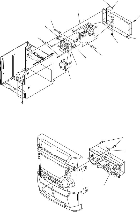
FRONT BOARD AND CENTER/REAR BOARD SECTION, DC FAN (M505)
3 four screws
(BVTP3 × 10)
5 three screws
(BVTP3 × 6)
qs FRONT board and CENTER/REAR board section
7 connector |
3 eight screws |
||
(BVTP3 |
× 10) |
||
(CN505) |
|||
|
|
||
9 holder
8 four screws
(3 × 30)
6 rear cover
5 three screws (BVTP3 × 6)
4
1 connector
9 holder |
(CN501) |
qa DC fan (M505)
0 main chassis holder
 2 three screws (PTPWH4 × 10)
MECH DECK (CWL-44-RR)
1 six screws (BVTP3 × 8)
2 harness
3 mech deck (CWL-44-RR)
8

CD TRAY |
1 two screws |
|
|
|
(KTP3 × 8) |
4 screw (BTP3 × 10)
5 bracket
8 CD tray
DECORD BOARD
6 DECORD board
1wire (flat type) (5core) (CN706)
3 connector (CN707)
5 connector (CN702)
2 top cabinet
1 two screws (KTP3 × 8)
3wire (flat type) (5core) (CN06)
6 screw (BTP3 × 10)
7 bracket
4three screws (BTP2.6 × 6)
2wire (flat type) (15core) (CN701)
9
BASE UNIT
4 screw (PTPWH3 × 8)
5 UD-cam
8 spring
2 flange screw
3 UD-gear
7 spring
6 spring
|
1 two screws |
9 base unit |
(PTPWH3 × 10) |
CASSETTE LID
cassette door
(Note: Four claws are used.)
10
SECTION 4
DIAGRAMS
4-1. NOTE FOR PRINTED WIRING BOARDS AND SCHEMATIC DIAGRAMS
Note on Printed Wiring Board:
•Y: parts extracted from the conductor side.
•b: Pattern from the side which enables seeing. (The other layers' patterns are not indicated.)
Note on Schematic Diagram:
•All capacitors are in µF unless otherwise noted. U: µF, pF: µµF 50 WV or less are not indicated except for electrolytics and tantalums.
•If a numeric value of capacitor is a decimal function, the preceding zero may be omitted.
(For example, .1 expresses 0.1)
•All resistors are in Ω and 1/4 W or less unless otherwise specified.
•f : internal component.
•2: nonflammable resistor.
•C: panel designation.
Note: |
Note: |
The components identi- |
Les composants identifiés par |
fied by mark 0or dotted |
une marque 0sont critiques |
line with mark 0are criti- |
pour la sécurité. |
cal for safety. |
Ne les remplacer que par une |
Replace only with part |
pièce portant le numéro |
number specified. |
spécifié. |
|
|
•U : B+ Line.
•V : B– Line.
•H: adjustment for repair.
•Voltages are taken with a VOM (Input impedance 10 MΩ ). Voltage variations may be noted due to normal production tolerances.
•Waveforms are taken with a oscilloscope.
Voltage variations may be noted due to normal production tolerances.
•Circled numbers refer to waveforms.
•Signal path.
F : FM f : AM
E : TAPE PLAY (DECK A) d : TAPE PLAY (DECK B)
G : TAPE REC
J : CD PLAY (ANALOG OUT) c : CD PLAY (DIGITAL OUT)
•Abbreviation
CND : Canadian model
• Circuit Boards Location
SW D board
SW B board
SW C board
DECORD board
MOTOR board
SW A board
PHOTO SOCKET board
MAIN board
FRONT board
PANEL board
H/P board
CENTER/REAR board
BACK UP board
11 11

HCD-BX6AV/DX6AV
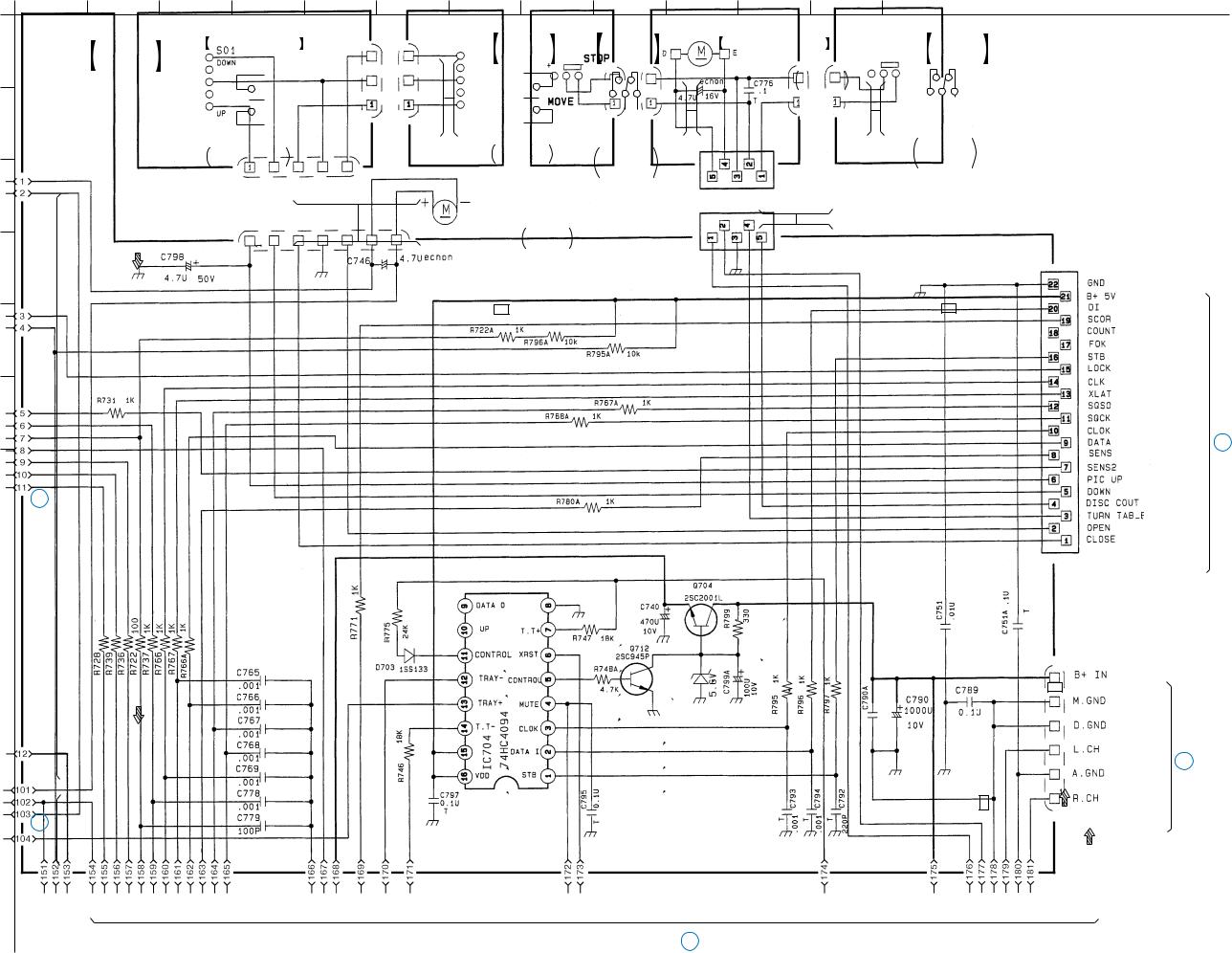
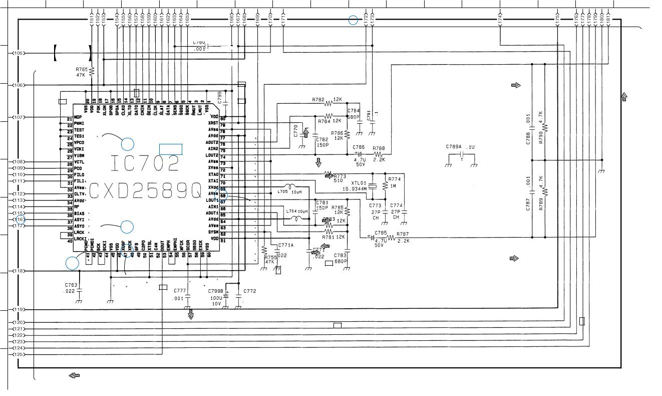
4-2. SCHEMATIC DIAGRAM – CD Section (1/4) – • See page 28 for Waveforms. • See page 29 for IC Block Diagram.
1 |
|
2 |
3 |
4 |
5 |
|
6 |
|
7 |
8 |
|
9 |
|
A |
|
|
|
|
|
|
|
|
|
|
|
|
|
|
|
|
|
|
|
|
DECORD BOARD |
(1/4) |
|
|
Q701 |
||
|
|
|
|
|
|
|
AUTOMATIC POWER |
||||||
|
|
|
|
|
|
|
|
|
|
|
|||
|
|
|
|
|
|
|
|
|
|
|
|
CONTROL |
|
B |
|
|
|
|
|
|
|
|
|
2.4 |
|||
|
|
|
|
|
|
|
|
|
5 |
||||
|
|
|
|
|
|
|
|
B+ |
|
|
4.8 |
||
C |
|
|
|
|
|
|
|
|
|||||
|
|
|
|
|
|
|
|
|
|
||||
|
|
|
|
|
|
|
|
|
|
|
|
||
|
|
B+ |
10 |
|
|
|
|
|
|
|
|
|
|
|
|
|
|
|
|
|
|
|
|
|
|||
|
|
|
|
|
|
|
|
|
|
|
|
|
|
D |
|
|
9 |
|
|
|
|
|
|
|
|
|
|
|
|
|
|
|
|
|
|
|
|
|
|
||
|
|
|
|
8 |
|
|
|
|
|
|
|
|
|
|
|
|
|
7 |
|
|
CN701 |
|
|
|
|
||
|
|
|
|
|
|
|
|
|
|
||||
|
|
|
|
|
|
15P |
|
|
|
|
|||
|
|
|
|
|
|
|
|
|
|
|
|||
E |
|
|
6 |
|
|
|
|
|
|
|
|
|
|
|
|
|
|
|
|
|
|
|
|
|
|
||
B+
F
G
|
0 |
|
|
|
|
|
OPTICAL |
|
H |
PICK-UP |
|
BLOCK |
100V |
|
|
(OPTIMA-7) |
|
|
|
100V |
|
|
|
I |
|
100V |
|
|
J |
C737 |
|
.01U |
||
|
K
05
10 |
11 |
12 |
13 |
14 |
15 |
16 |
C701
47
16V
|
|
|
|
|
|
|
C704 |
|
|
|
|
|
|
|
|
|
|
|
|
|
|
|
0.033 |
|
|
|
|
|
|
|
|
|
|
|
|
|
|
|
100V |
|
|
|
100V |
|
|
|
|
|
|
|
|
|
|
|
|
|
100V |
|
|
100V |
|
||
|
2.5 |
4.8 |
2.6 |
1.8 |
1.8 |
|
2.5 1.2 |
|
4.3 1.6 |
|
|||||
|
2.5 |
0 |
|
2.8 |
0.1 |
||||||||||
|
|
|
|
|
|
|
|
|
|
|
|
|
|
||
|
|
|
|
|
|
|
|
|
|
|
|
|
|
|
|
|
|
|
|
|
|
|
|
|
|
|
|
|
|
|
5 |
2.5 |
|
|
|
|
|
|
2 |
|
|
|
|
|
|
|
0 |
2.5 |
|
|
|
|
|
|
|
|
|
|
|
|
|
5 |
|
|
|
|
|
|
|
|
|
|
|
|
|
|
|
|
|
|
|
|
|
|
|
|
|
|
|
|
|
|
|
|
5 |
|
3 |
|
|
|
|
|
|
|
|
|
|
|
|
0 |
|
2.5 |
|
|
|
|
|
|
|
|
|
|
|
|
5 |
||
|
|
|
|
|
|
|
|
|
|
|
|
|
|
|
|
1.8 |
|
|
|
|
|
|
|
|
|
|
|
|
|
|
5 |
2.5 |
|
|
|
|
|
|
|
|
|
|
|
|
|
|
5 |
1.9 |
|
|
|
|
|
|
|
|
|
|
|
|
|
|
4.9 |
|
|
|
|
|
|
|
|
|
|
|
|
|
|
|
1.3 |
2.4 |
|
|
|
|
|
IC701 |
|
|
|
|
|
2.5 |
|||
2.3 |
|
|
|
|
|
|
|
|
|
|
|
|
|
|
2.5 |
1 |
|
RF AMP, FOCUS/TRACKING |
|
||||||||||||
2.5 |
|
|
2.5 |
||||||||||||
|
|
|
ERROR AMP |
|
|
|
|
||||||||
1.9 |
|
|
|
|
|
|
|
|
|||||||
100V |
|
|
|
|
|
|
|
|
|
|
|
|
|
|
|
|
|
|
|
|
|
|
|
|
|
|
|
|
|
|
|
|
2.6 2.6 |
2.3 2.4 |
2.2 |
2.5 |
2.5 |
50V |
|
|
100V |
2.5 |
0.8 |
2.5 |
2.5 |
||
|
|
|
|
|
|
|
|
|
2.7 |
0.033 |
|
|
|
|
|
|
|
|
|
|
|
|
|
|
|
|
|
|
|
||
|
|
|
|
|
|
|
|
|
|
|
|
2.4 |
|
|
|
|
|
0.1 100V |
|
0.1 100V |
|
100V |
|
|
|
|
|
|
|
|
|
100V
100V
B+
B+
1 (Page 13)
B+ |
DECORD |
|
BOARD |
||
|
||
|
(2/4) |
2 DECORD BOARD (3/4)
(Page 14)
12 12
•Voltages and waveforms are dc with respect to ground under no-signal conditions.
no mark : CD PLAY
The components identified by mark 0or dotted |
Les composants identifiés par une marque 0sont |
line with mark 0are critical for safety. |
critiques pour la sécurité. Ne les remplacer que |
Replace only with part number specified. |
par une pièce portant le numéro spécifié. |
|
|
4-3. SCHEMATIC DIAGRAM – CD Section (2/4) – |
|
|
|
|
|
|
|
|
|||
1 |
2 |
3 |
4 |
5 |
6 |
7 |
8 |
9 |
10 |
11 |
12 |
A |
DECORD |
SW D BOARD |
CN16_ |
CN16 |
SW C |
SW A |
MOTOR BOARD |
|
|
3P |
3P |
BOARD |
BOARD |
M103 CN19 |
|||
|
BOARD |
|
||||||
|
|
|
|
|
|
|
2P |
|
|
(2/4) |
|
|
|
|
|
|
DISC |
|
|
|
|
|
|
|
TABLE TURN |
|
|
|
|
|
|
|
|
|
C01 |
B |
|
|
|
|
|
|
|
50 |
|
|
|
|
S02 |
|
CN18 |
|
|
|
|
|
|
|
|
CN18 |
||
|
|
S01 |
|
|
S04 |
2P |
||
|
|
|
|
OPEN/CLOSE |
||||
|
|
OPTICAL PICK-UP |
|
|
TURN TABLE |
2P |
||
|
|
UP/DOWN DETECT |
|
|
DETECT |
OPERATION |
|
|
|
|
|
|
|
|
DETECT |
|
|
C |
|
CN05_ |
|
|
|
|
|
CN06_ |
|
|
5P |
|
|
|
|
|
|
|
|
|
|
|
|
|
5P |
|
|
|
|
|
|
M104 |
|
|
|
|
|
|
|
|
|
|
|
|
|
|
CN707 |
|
|
DISC TRAY |
|
|
|
|
|
|
|
SLIDE |
|
|
|
|
|
|
7P |
|
|
|
|
|
|
|
|
|
|
|
|
|
|
|
D |
|
|
|
|
|
|
|
CN706 |
|
|
|
|
35V |
|
|
|
5P |
|
|
|
|
|
|
|
|
|
|
|
|
|
|
B+ |
|
|
|
E |
|
|
|
|
|
|
|
|
F
G |
1 |
|
|
|
|
|
|
|
|
|
|
|
|
|
|
|
|
|
|
|
|
|
|
|
|
|
|
|
|
|
|
|
|
|
|
|
|
|
DECORD |
|
|
|
|
|
|
|
|
|
|
|
|
|
|
|
|
|
|
BOARD |
|
|
|
|
|
|
|
|
|
|
|
|
|
|
|
|
|
|
|
|
|
|
|
|
|
|
|
|
|
|
|
|
|
|
|
|
|
(1/4) |
|
|
|
|
|
|
|
|
|
|
|
|
|
|
|
|
|
|
(Page |
|
|
|
|
|
|
|
|
|
|
|
|
|
|
|
|
|
H |
12) |
|
|
|
|
|
|
|
|
|
|
|
|
|
|
|
|
|
|
|
|
|
|
|
|
|
|
|
|
|
|
|
|
|
|
|
|
|
|
|
|
|
|
|
|
|
|
|
|
|
|
|
|
Q704 |
|
|
|
|
|
|
|
|
|
|
|
|
|
|
|
B+ |
|
|
REGULATOR |
|
|
|
|
|
|
B+ |
|
|
|
|
|
|
|
|
|
|
|
|
|
|
|
|
|
|
|
|
|
|
|
|
|
|
|
|
|
|
|
|
|
|
|
|
|
|
|
|
|
|
|
|
|
|
|
|
|
|
||
|
|
|
|
|
|
|
|
|
|
|
|
|
|
|
|
|
||
|
|
|
|
|
|
|
|
|
|
|
|
|
4.9 |
8 |
|
B+ |
||
I |
12K |
12K |
12K |
|
|
|
0 |
|
|
|
|
|
|
|
||||
|
|
|
|
|
|
|
|
|
|
|
||||||||
|
|
|
|
|
|
|
|
|
|
|
|
|
|
|
|
|
|
|
|
|
|
0 |
|
|
|
5 |
|
0 |
5.6B2S-UDZ |
0 |
|
|
|||||
|
|
|
|
|
|
|
|
|
||||||||||
|
|
|
0 |
|
|
|
0 |
|
|
|
|
|||||||
J |
|
|
|
|
|
|
|
D706 |
|
|
|
|||||||
|
|
|
|
|
|
|
|
|
|
|
|
|||||||
|
|
|
|
|
|
|
|
|
|
|
0 |
|
|
|
|
|
|
|
|
|
|
0 |
|
|
|
0 |
|
|
|
|
|
|
|
||||
|
|
|
0 |
|
|
|
|
4.3 |
|
|
|
|
|
|
||||
|
|
|
|
|
|
|
|
|
|
|
|
|
||||||
K |
|
|
5.7 |
|
|
|
|
0.6 |
|
|
|
|
|
|
||||
|
|
|
|
|
|
|
|
|
|
|
|
|
|
|
|
|
|
|
|
|
|
|
|
B+ |
5.7 |
|
|
|
|
0 |
|
|
|
|
|
|
|
|
|
|
|
|
|
|
|
|
|
|
|
|
|
|
|
|||
|
3 |
|
|
|
|
|
|
|
|
|
Q712 |
|
|
|
||||
|
|
|
|
|
|
|
|
|
|
|
|
|||||||
|
|
|
|
|
|
|
|
|
|
|
|
|
|
|
|
|
||
|
|
|
|
|
|
|
|
|
|
|
|
|
|
|
|
|
||
|
|
|
|
|
|
|
|
IC704 |
|
|
|
|
REGULATOR |
|
||||
|
DECORD |
|
|
|
|
|
|
|
|
|
|
CONTROL SWITCH |
|
|||||
L |
|
|
|
|
|
|
|
|
|
|
|
|
||||||
|
|
|
|
|
|
DISC TRAY SLIDE/ |
|
|
|
|||||||||
BOARD |
|
|
|
|
|
|
|
|
|
|
|
|
|
|
||||
(3/4) |
|
|
|
|
|
|
|
|
|
|
|
|
|
|
||||
|
|
|
|
|
|
|
DISC TRAY TURN MOTOR |
|
|
|
|
|
|
|
|
|||
|
(Page |
|
|
|
|
|
|
|
|
|
|
|
|
|
|
|||
|
|
|
|
|
|
|
|
CONTROL |
|
|
|
|
|
|
|
|
||
|
14) |
|
|
|
|
|
|
|
|
|
|
|
|
|
|
|
||
|
|
|
|
|
|
|
|
|
|
|
|
|
|
|
|
|
|
|
|
05 |
|
|
|
|
|
|
|
|
|
|
|
|
|
|
|
|
|
M
4 |
DECORD |
(Page 15) |
BOARD (4/4) |
13 13
HCD-BX6AV/DX6AV
13 |
14 |
15 |
16 |
17 |
SW B
CN19 BOARD
2P
S03
TURN TABLE
POSITION
DETECT
B+
CLOK
|
A (Page 23) |
|
PANEL |
1 |
BOARD |
CN605 |
PIC DOWN
DISC COUNT
CN705
22P
CN704
6P
B+
+7.5V
0.022
B (Page 20)
MAIN
BOARD (3/4)
CN304
B+
•Voltages are dc with respect to ground under no-signal conditions.
no mark : CD PLAY
HCD-BX6AV/DX6AV
4-4. SCHEMATIC DIAGRAM – CD Section (3/4) – |
|
• See page 29 for IC Block Diagram. |
|
||||||||||||
1 |
|
2 |
|
3 |
|
4 |
|
5 |
|
6 |
|
7 |
|
|
8 |
|
|
|
|
|
|
|
|||||||||
|
|
|
|
|
|
|
|
|
|
|
|
(Page 12) |
|||
A |
|
|
|
|
|
|
|
|
|
|
2 |
DECORD |
|||
|
|
|
|
|
|
|
|
|
|
BOARD (1/4) |
|||||
B |
|
|
|
|
DECORD BOARD |
(3/4) |
|
|
|
|
|
|
|
|
|
|
|
|||
|
|
|
|
|
|
|
|
|
|
|
|
|
|
|
|
|
|
|
|
|
|
|
|
|
|
|
|
|
|
|
|
|
|
|
|
|
|
|
|
|
|
|
|
|
|
|
|
|
|
|
|
|
|
|
|
|
|
|
|
|
|
|
|
|
|
|
|
|
|
|
|
|
B+ |
|
|
|
|
|
|
|
|
|
|
C |
|
|
|
|
|
|
|
|
|
|
|
|
|
|
|
C740A |
|
|
|
|
|
|
|
|
|
|
|
|
|
|
|
|
|
|
|
|
0.0047 |
|
|
|
|
|
|
|
|
|
|
|
|
|
|
|
|
|
|
|
|
2.8 |
|
|
|
|
|
|
|
|
|
|
|
|
|
|
|
|
|
|
|
|
2.8 |
|
|
|
|
|
|
|
|
|
|
|
|
|
|
|
|
|
|
|
|
|
|
|
||
D |
|
|
|
|
|
|
|
|
|
|
|
|
|
|
C740B |
2.8 |
|
2.8 |
|
|
|
|
|
|
|
|
|
|
|
|
|
|
|
|
0.0047 |
|
|
||||
|
|
|
|
|
|
|
|
|
|
|
|
|
|
|
|
|
||||
|
|
|
|
|
|
|
|
|
|
|
|
|
|
|
|
|
|
|
||
|
|
|
|
|
|
|
CN702_ |
|
CN702 |
|
2.8 |
0 |
2.8 |
|||||||
|
|
|
|
|
|
|
|
|
|
|
||||||||||
|
|
|
|
|
|
|
6P |
|
6P |
|
|
|
0 |
|
|
|||||
|
|
|
|
|
|
|
|
|
|
|
||||||||||
|
|
|
|
|
|
|
|
|
|
|
|
|
|
|
|
|
|
|
|
|
E |
|
|
|
|
|
|
|
|
|
|
|
|
|
|
|
2.5 |
|
4 |
|
|
|
|
|
|
|
|
M101 |
|
|
|
|
|
|
|
|
|
|
|
|
||
|
|
|
|
|
|
|
|
|
|
|
|
|
|
|
|
|
|
|
|
|
|
|
|
|
|
|
|
(SPINDLE) |
|
|
|
|
|
|
|
|
2.5 |
|
|
|
|
|
|
|
|
|
|
|
|
|
|
|
|
|
|
|
|
|
|
|
|
|
|
|
|
|
|
|
|
|
|
|
|
|
|
|
|
|
8 |
|
|
|
|
|
|
|
|
|
|
|
|
|
|
|
|
|
|
|
|
|
|
|
|
|
|
|
|
|
|
|
|
|
|
|
|
|
|
|
|
|
|
|
|
|
|
F |
M102 |
|
|
|
|
|
|
|
|
|
IC703 |
|
|
8 |
|
|
|
|
||
|
|
S05 |
|
|
|
|
B+ |
|
2.5 |
|
|
|||||||||
|
(SLED) |
|
|
|
|
FOCUS/TRACKING |
|
|
|
|
|
|
||||||||
|
|
(LIMIT) |
|
|
|
|
|
|
|
|
||||||||||
|
|
|
|
|
|
|
|
|
|
|
|
|
||||||||
|
|
|
|
|
|
|
|
|
|
|
|
COIL DRIVE, |
|
|
|
8 |
|
|
||
|
|
|
|
|
|
|
|
|
|
|
|
SPINDLE/SLED/ |
|
|
|
|
|
|
||
|
|
|
|
|
|
|
|
|
|
|
|
|
|
|
|
|
|
|||
|
|
|
|
|
|
|
|
|
|
DISC TABLE SLIDE/ |
|
|
|
2.5 |
B+ |
|||||
|
|
|
|
|
|
|
|
|
|
|
|
|
|
|||||||
|
|
|
|
|
|
|
|
|
|
|
DISC TRAY TURN |
|
|
|
|
|||||
G |
|
|
|
|
|
|
|
|
|
|
|
|
|
|
|
|
||||
|
|
|
|
|
|
|
|
|
|
|
MOTOR DRIVE |
|
0 |
|
2.5 |
|
||||
|
|
|
|
|
|
|
|
|
|
|
|
|
|
|
|
|
|
|||
|
|
|
|
|
|
|
|
|
|
|
|
|
|
|
|
0 |
|
2.8 |
C740D |
|
|
|
|
|
|
|
|
|
|
|
|
|
|
|
|
|
|
0.0047 |
|
||
|
|
PHOTO SOCKET |
|
|
|
|
|
|
|
|
2.8 |
2.8 |
|
|||||||
H |
|
BOARD |
|
|
|
|
|
|
|
|
2.8 |
2.8 |
|
|
||||||
|
|
B+ |
|
|
|
|
|
|
|
|||||||||||
|
|
|
|
|
|
|
|
|
|
|
|
|
|
|
|
|
||||
|
|
|
|
|
2.6 |
|
|
|
|
|
|
|
|
|
|
|
|
|||
|
|
|
|
3 |
|
|
|
|
|
|
|
|
|
|
|
2.8 |
|
|
||
|
|
|
|
|
|
|
|
|
|
|
|
|
|
|
|
|||||
|
|
|
|
|
|
|
|
|
|
|
|
|
|
|
|
|
|
|
||
|
|
PH701 |
2 |
4.9 |
|
|
|
|
|
|
|
|
|
|
|
|
|
|
||
|
|
|
|
|
|
|
|
|
|
|
|
|
|
|
|
|
|
|||
I |
|
TOTX178 |
|
|
|
|
|
|
|
|
|
|
|
|
|
|
|
|
|
|
|
|
|
1 |
|
|
|
|
|
|
|
|
|
|
|
|
|
|
|
|
|
|
|
|
|
|
|
|
|
|
|
|
|
|
|
|
|
|
|
|
|
|
|
|
|
|
|
|
|
|
CN703 |
|
|
|
|
|
|
||||||
|
|
CD DIGITAL |
|
|
CN703_ |
|
|
|
|
|
|
|||||||||
|
|
|
|
3P |
|
|
|
|
|
|
|
|
|
|
|
|
||||
|
|
OUT (OPTICAL) |
|
|
3P |
|
|
|
|
|
|
|
|
|
|
C740C |
||||
|
|
|
|
|
|
|
|
|
|
|
|
|
|
|
||||||
|
|
|
|
|
|
|
|
|
|
|
|
|
|
|
|
|
|
|
||
|
|
|
|
|
|
|
|
|
|
|
|
|
|
|
|
|
|
|
0.0047 |
|
J |
|
OPTICAL |
|
PH701 |
|
|
|
|
|
|
|
|
|
|
|
|
||||
|
|
|
|
|
|
|
|
|
|
|
|
|
|
|
|
|||||
|
TRANSCEIVER |
|
|
|
|
|
|
|
|
|
|
|
|
|
||||||
K
05
9 |
10 |
11 |
12 |
13 |
14 |
DECORD
3 BOARD (2/4)
(Page 13)
B+
18K |
18K |
|
5 |
100V |
DECORD |
|
BOARD |
|
(4/4) |
(Page 15)
B+
100V
100V
B+
B+
•Voltages are dc with respect to ground under no-signal conditions.
no mark : CD PLAY
14 14
HCD-BX6AV/DX6AV
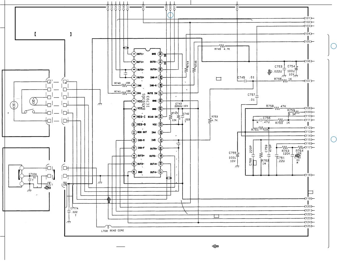
4-5. SCHEMATIC DIAGRAM – CD Section (4/4) – • See page 28 for Waveforms. • See page 29 for IC Block Diagram.
|
1 |
2 |
|
3 |
|
|
4 |
|
|
|
5 |
|
|
|
|
|
6 |
7 |
8 |
9 |
10 |
11 |
12 |
13 |
14 |
15 |
15 |
16 |
|
|
|
|
|
|
|
|
|
|
|
|
|
|
|
|
|
|
|
|
4 |
DECORD |
(Page 13) |
|
|
|
|
|
|
A |
|
|
|
|
|
|
|
|
|
|
|
|
|
|
|
|
|
|
|
BOARD (2/4) |
|
|
|
|
|
|
||
|
|
|
|
|
|
|
|
|
|
|
|
|
|
|
|
|
|
|
|
|
|
|
|
|
|
|
|
|
|
|
DECORD |
|
|
|
|
|
|
|
|
|
|
|
|
|
|
|
|
|
|
|
|
|
|
|
|
|
|
B |
|
BOARD |
(4/4) |
|
|
|
|
|
|
|
|
|
|
|
|
C780 |
|
|
|
|
|
|
|
|
|
|
|
|
|
|
|
|
|
|
|
|
|
|
|
|
|
|
|
|
|
|
|
|
|
|
|
|
|
|
|
||
|
|
|
|
|
|
|
|
|
|
|
|
|
|
|
|
|
|
B+ |
|
|
|
|
|
|
|
|
|
|
|
|
|
|
|
|
|
B+ |
|
|
|
|
|
|
|
|
|
|
|
|
|
|
|
|
|
|
|
|
|
C |
|
B+ |
|
|
|
|
|
|
|
|
|
|
|
|
|
|
|
B+ |
|
|
|
|
|
|
|
|
|
|
|
|
|
|
|
4.9 |
0.1 |
4.8 |
5 |
0 |
0.1 |
0.1 0.1 |
5 |
5 |
0 |
0 |
0 |
5 |
0.022 |
|
|
|
|
|
|
|
|
|
|
|
|
|
|
|
|
|
|
|
|
|
|
|
|
|
|
|
|
|
|
|
|
|
|
|
|
|
|
|
|
|
|
|
2.4 |
|
|
|
|
|
|
|
|
|
|
|
|
|
|
|
|
|
|
|
|
|
|
|
|
D |
|
|
|
|
4 |
|
|
|
|
|
|
|
|
|
|
|
4.9 |
|
|
|
|
|
|
|
|
|
|
|
|
|
|
|
|
|
|
|
IC702 |
|
|
|
|
|
|
5 |
|
|
|
|
|
|
|
|
|
|
|||
|
|
|
|
|
|
|
|
|
|
|
|
|
|
|
|
|
|
|
|
|
|
|
|
|
|
|
||
|
|
|
|
|
|
|
DIGITAL SIGNAL PROCESSOR, |
|
|
|
4.9 |
|
|
|
|
|
|
|
|
|
|
|||||||
|
|
|
|
|
|
|
CLV SERVO, D/A CONVERTER |
|
|
|
2.2 |
|
|
|
|
|
|
|
|
|
|
|||||||
|
|
|
|
|
|
|
|
|
|
|
|
|
|
|
|
|
|
|
|
|
|
|
|
|
|
|
|
|
E |
|
|
|
|
|
|
|
|
|
|
|
|
|
|
|
|
|
2.2 |
|
|
|
|
|
|
|
|
|
|
|
|
4.8 |
|
|
|
|
|
|
|
|
|
|
|
|
|
|
2.2 |
|
|
|
|
|
|
|
|
|
|
|
|
|
|
2.5 |
|
|
|
|
|
|
|
|
|
|
|
|
|
|
|
|
|
|
|
|
|
|
|
|
|
|
|
|
2.6 |
|
|
|
|
|
|
|
|
|
|
|
|
|
7 |
|
|
|
|
|
|
|
|
|
|
|
|
|
|
2.5 |
|
|
|
|
|
|
|
|
|
|
|
|
|
2.8 |
|
|
|
|
|
|
|
|
|
|
|
|
|
|
|
|
|
|
|
|
|
|
|
|
|
|
|
|
|
2.1 |
|
|
|
|
|
|
|
|
|
|
F |
|
|
2.6 |
|
|
|
|
|
|
|
|
|
|
|
|
|
|
4.9 |
|
|
|
|
|
|
|
|
|
|
5 |
|
4.9 |
|
|
|
|
|
|
|
|
|
|
|
|
|
|
|
|
|
|
|
|
|
|
|
|
|
|
|
|
2.5 |
|
2 |
|
|
|
|
|
|
|
|
|
|
|
|
2.2 |
|
|
|
|
|
|
|
|
|
|
|
|
DECORD |
|
|
|
|
|
|
|
|
|
|
|
|
|
|
|
|
|
|
|
|
|
|
|
|
|||
|
|
0.8 |
|
|
|
|
|
|
|
|
|
|
|
|
|
2.1 |
|
|
|
|
|
|
|
|
|
|
||
|
BOARD |
|
|
|
|
|
|
|
|
|
|
|
|
|
|
|
|
|
|
|
|
|
|
|
|
|||
|
(3/4) |
|
2.5 |
|
|
|
|
|
|
|
|
|
|
|
|
|
|
2.1 |
|
|
|
|
|
|
|
|
|
|
|
(Page 14) |
|
|
|
|
|
|
|
|
|
|
|
|
|
|
|
|
|
|
|
|
|
|
|
|
|
||
|
|
2.6 |
|
6 |
|
|
|
|
|
|
|
|
|
|
|
|
4.9 |
|
|
|
|
|
|
|
|
|
|
|
G |
|
5 |
|
|
|
|
|
|
|
|
|
|
|
|
|
|
0 |
|
|
|
|
|
|
|
|
|
|
|
|
|
|
|
|
|
|
|
|
|
|
|
|
|
|
|
|
|
|
|
|
|
|
|
|
|
|
||
|
|
2.5 |
|
|
|
|
|
|
|
|
|
|
|
|
|
|
4.9 |
B+ |
B+ |
|
|
|
|
|
|
|
|
|
|
|
|
|
|
|
|
|
|
|
|
|
|
|
|
|
|
|
|
|
|
|
|
|
|
|
|
|
|
|
|
|
|
|
|
|
4.9 |
|
|
|
|
2.6 |
|
|
|
|
0 |
|
|
|
|
|
|
|
|
|
|
|
|
|
|
|
0 |
2.6 |
|
|
B+ |
|
|
|
0 |
|
|
|
|
|
|
|
|
|
|
|
|
|
|||
H |
|
|
|
|
|
|
|
|
|
|
|
|
|
|
|
|
|
|
|
|
|
|
|
|||||
|
|
|
|
|
|
|
|
|
|
|
|
|
|
|
|
|
|
|
|
|
|
|
|
|
|
|
|
|
|
|
|
|
|
|
|
|
|
|
|
|
|
|
|
|
|
|
|
0.022 |
|
|
|
|
|
|
|
B+ |
|
|
|
|
|
|
|
|
|
|
|
|
|
|
|
|
|
|
|
|
|
B+ |
|
|
|
|
|
|
|
|
I |
|
|
|
|
|
|
|
|
|
|
|
|
|
|
|
|
|
|
|
|
|
|
|
|
|
|
|
|
|
|
|
|
|
|
|
|
|
|
|
|
|
|
|
|
|
|
|
|
|
|
|
|
|
|
|
|
|
J |
|
|
|
|
|
|
|
|
|
|
|
|
|
|
|
|
|
|
|
|
|
|
|
|
|
|
|
|
|
|
05 |
|
|
|
|
|
|
|
|
|
|
|
|
|
|
|
|
|
|
|
|
|
|
|
|
|
|
• Voltages and waveforms are dc with respect to ground under no-signal conditions.
no mark : CD PLAY
15 15
HCD-BX6AV/DX6AV
4-6. |
PRINTED WIRING BOARDS – CD Section – |
• See page 11 for Circuit Boards Location. |
|
|
|
|
|
|
|
|
|
|
|
|
|
|
|
|
|
|
|
|
|
|
|
|
|
|
|
|
|
|
|
|
|
|
|
|
|
|
|
|
|
|
|
|
|
||||||||||||||||||||||||||||||||||||||||||||
|
|
|
|
|
|
|
|
|
|
|
|
|
|
|
|
|
|
|
|
|
|
|
|
|
|
|
|
|
|
|
|
|
|
|
|
|
|
|
|
|
|
|
|
|
|
|
|
|
|
|
|
|
|
|
|
|
|
|
|
|
|
|
|
|
|
|
|||||||||||||||||||||||||
|
|
1 |
|
|
|
2 |
|
|
|
|
|
|
|
|
3 |
|
|
|
|
|
|
|
|
|
|
4 |
|
|
|
|
|
|
|
|
|
5 |
|
6 |
7 |
|
|
|
8 |
|
|
|
|
|
9 |
|
|
10 |
|
11 |
|
|
|
12 |
|
|
|
|
|
|
|
||||||||||||||||||||||||||
|
A |
|
|
|
|
|
|
|
|
|
|
|
|
|
|
|
SW B BOARD |
|
|
|
|
|
|
|
|
|
|
|
|
|
|
|
|
|
|
|
|
|
|
|
SW D BOARD |
|
|
|
|
SW C BOARD |
|
|
|
|
|
|
|
|
|
|
|
||||||||||||||||||||||||||||||||||
|
MOTOR BOARD |
|
|
|
|
|
|
|
|
|
|
|
|
|
|
|
|
|
|
|
|
|
|
|
|
|
|
|
|
|
|
|
|
|
|
|
|
|
|
|
|
|
|
|
|
|
|
|
|
|
|
CN16 |
|
|
|
|
|
|
|
|
|
|
|
|
|
|
|
|
|
|
|
||||||||||||||||||||
|
|
|
|
|
|
|
|
|
|
|
|
|
|
|
|
|
|
|
|
|
|
|
|
|
|
|
|
|
|
|
|
|
|
|
|
|
|
|
|
|
|
|
|
|
|
|
|
|
|
|
|
|
|
|
|
|
|
|
|
|
|
|
|
|
|
|
|
|
|
|
|
|
|
||||||||||||||||||
|
|
|
M103 |
|
|
|
|
|
|
|
|
|
|
|
|
CN19 |
|
|
|
|
|
|
|
|
|
|
|
|
|
|
|
|
|
|
|
|
|
|
|
|
|
|
|
|
|
|
|
|
|
|
|
|
|
|
|
|
|
|
|
|
|
|
|
|
|
|
|
|
|
|
|
|
|
|
|
|
|
|
|
|
|
|
|
||||||||
|
|
(DISC TABLE TURN)CN19 |
|
|
|
|
|
|
|
1 2 |
|
|
|
|
|
|
|
|
S03 |
|
|
|
|
|
|
|
|
|
|
|
|
|
|
|
|
|
|
|
|
|
|
|
|
|
|
|
|
|
|
|
|
|
|
|
|
|
|
|
|
1 |
|
|
|
|
|
|
|
|
|
|
|
|
|
|
|
|
|
|
|
|
|
||||||||||
|
|
|
|
|
|
|
|
|
|
|
|
|
|
|
|
|
|
|
|
|
|
|
|
|
|
|
|
|
|
|
|
|
|
|
|
|
|
|
|
|
|
|
|
|
|
|
|
|
|
|
|
|
|
|
|
|
|
|
|
|
|
|
|
|
|
|
|
|
|
|
|
|
|
|
|
|
|
||||||||||||||
|
|
|
|
|
|
|
|
|
2 |
1 |
|
|
|
|
|
|
|
|
|
|
|
|
|
|
|
|
|
|
|
|
|
11 |
|
|
|
|
|
|
|
|
|
|
|
|
|
|
|
|
|
|
|
|
|
|
|
|
|
|
|
|
|
|
|
|
|
|
|
|
3 |
|
|
|
|
|
|
|
|
|
|
|
|
|
|
|
|
|
|
|
|
|
|
|
|
M |
|
|
|
|
|
|
|
|
|
|
|
|
|
|
|
|
|
|
|
|
|
|
|
|
|
|
(11) |
|
|
|
|
|
|
|
|
|
|
|
|
|
|
|
|
|
3 |
|
|
|
|
|
|
|
|
|
|
|
|
|
|
|
|
|
|
|
|
|
|
|
|
|
|
|
|
|
|
|
|
|
|
|
|
|
|
||||||
|
|
|
|
|
|
|
|
|
|
|
|
|
|
|
|
|
|
|
|
|
|
|
|
|
|
|
|
|
|
|
|
|
|
|
|
|
|
|
|
|
|
|
|
|
|
|
|
|
|
|
|
|
|
|
|
|
|
|
|
|
|
|
|
|
|
|
|
|
|
|
|
|
|
|
|
|
|
||||||||||||||
|
|
|
|
|
CN18 |
|
|
2 |
|
|
|
|
|
|
|
|
|
|
|
|
|
|
|
|
|
|
|
|
|
|
|
|
|
|
|
|
|
|
|
|
|
|
|
|
1 |
|
|
|
|
|
|
S01 |
|
|
|
|
|
|
|
|
|
|
|
|
|
|
|
|
|
|
|
|
|
|
|
|
|
|
|
|
|
||||||||||
|
|
|
|
|
|
1 |
|
|
|
|
|
1-674-789- |
|
|
|
|
|
|
|
|
|
|
|
|
|
|
|
|
|
|
|
|
|
|
|
|
|
|
|
|
|
|
|
|
|
|
|
|
|
|
|
|
|
|
|
S02 |
|
|
|
|
|
|
|
|
|
|
|
|
|
|
|
|
|
|
|
|
|
||||||||||||||
|
|
|
|
|
|
|
|
|
|
|
|
|
|
|
|
|
|
|
|
|
|
|
|
|
|
|
|
|
|
|
|
|
|
|
|
|
|
|
|
|
|
|
|
|
|
|
|
|
|
|
|
|
|
|
|
|
|
|
|
|
|
|
OPTICAL |
|
|
|
|
|
|
|
|
|
|
|
|
|
|
|
|
|
|
|
|
|
|
|
|
|
|||
|
|
|
|
|
C01 |
|
|
|
|
|
|
|
|
|
|
|
|
|
|
|
|
|
|
|
|
|
|
|
|
|
|
|
|
|
|
|
|
|
|
|
|
|
|
|
|
|
|
|
CN16 |
CN05 |
|
|
|
|
|
|
|
|
|
|
|
|
|
|
|
|
|
|
|
|
|
|
|
|
|
|
|
|
|||||||||||||
|
B |
|
|
|
|
|
|
|
|
|
|
|
|
|
|
TURN TABLE |
|
|
|
|
SW A BOARD |
|
|
|
|
|
|
|
|
|
|
|
5 |
|
|
1 |
|
|
|
|
PICK-UP |
|
|
|
|
|
|
|
|
|
|
|
OPEN/CLOSE |
|
|
|
|
|
|
|
|
|
|
|
|||||||||||||||||||||||||||
|
|
|
|
|
|
|
|
|
|
|
|
|
|
|
|
DETECT |
|
|
|
|
|
|
|
|
|
|
|
|
|
|
|
|
|
|
|
|
|
DETECT |
|
|
|
|
|
|
|
|
|
|
|
|
|
|
|
|
|
|
|
|
|
|
|
|
|
||||||||||||||||||||||||||||
|
|
4 |
2 |
|
|
|
|
|
|
|
|
POSITION |
|
|
|
|
|
|
|
|
CN18 |
|
S04 |
|
|
|
|
|
|
|
|
|
|
|
|
|
|
|
|
|
UP/DOWN |
|
|
|
|
|
|
|
|
|
|
|
|
DETECT |
|
|
|
|
|
|
|
|
|
|
|
||||||||||||||||||||||||||
|
|
|
|
|
|
|
|
|
|
|
|
|
|
|
|
|
|
|
|
|
|
|
|
|
|
|
|
|
|
|
|
|
|
|
|
|
|
|
|
|
|
|
|
|
|
|
|
|
|
|
|
|
|
|
|
|
|
|
|
|
|
|
|
|
|
|
|
|
|
|
|
|
|
|
|
|
|||||||||||||||
|
|
|
|
|
|
|
|
|
|
|
|
|
|
|
|
|
|
|
|
|
|
|
|
|
|
|
|
|
|
|
1 2 |
|
|
|
|
|
|
|
|
|
|
11 |
|
|
|
|
|
|
|
|
|
|
|
|
|
|
|
|
|
|
|
11 |
|
|
|
|
|
|
|
|
|
|
|
|
|
|
|
|
|
|
|
|
|
|
|
|
|
|
|
||
|
|
5 |
|
1 |
|
CN06 |
11 |
|
|
|
|
|
|
|
|
|
|
|
|
|
|
|
|
|
|
|
|
|
|
|
|
|
|
|
(11) |
|
|
|
|
|
|
|
|
|
|
|
|
|
|
|
|
|
|
|
|
|
|
|
|
|
|
|
|
11 |
|
|
|
|
|
|
|
|
|
|
|
|
|
|
|
||||||||||||
|
|
|
|
|
|
|
|
|
|
|
|
|
|
|
|
|
|
|
|
|
|
|
|
|
|
|
|
|
|
|
|
|
|
|
|
|
|
|
|
|
|
|
|
|
|
|
|
|
|
1-674-791- |
(11) |
|
|
|
|
|
|
|
|
|
|
|
|
|
|
|
|
|
|
|
|||||||||||||||||||||
|
|
|
|
|
|
|
|
|
|
|
|
|
|
|
(11) |
|
|
|
|
|
|
|
|
|
|
|
|
|
|
|
|
|
|
|
|
|
|
|
|
|
|
|
|
|
|
|
|
|
|
|
|
|
|
|
|
|
|
|
|
|
|
|
|
|
|
|
|
|
|
|
|
|
|
|
|
|
|
|
|
|
|
|
|||||||||
|
|
|
|
|
|
|
|
|
1-674-792- |
|
|
|
|
|
|
|
|
|
|
|
|
|
|
1-674-788- |
|
|
|
|
|
|
|
|
|
|
A |
PANEL BOARD |
1-674-790- |
|
(11) |
|
|
|
|
|
|
|
|
|
|
|
|
|
|
|
|||||||||||||||||||||||||||||||||||||
|
|
|
|
|
|
|
|
|
|
|
|
|
|
|
|
|
|
|
|
|
|
|
|
|
|
|
|
|
|
|
|
|
|
|
|
|
|
|
|
|
|
|
|
|
|
|
|
|
|||||||||||||||||||||||||||||||||||||||||||
|
|
|
|
|
|
|
|
|
|
|
|
|
|
|
|
|
|
|
|
|
|
|
|
|
|
|
|
|
|
|
|
|
|
|
|
|
|
|
|
|
|
|
|
|
|
|
|
|
|
|
|
|
|
|
|
||||||||||||||||||||||||||||||||||||
|
|
|
|
|
|
|
|
|
|
|
|
|
|
|
|
|
|
|
|
|
|
|
|
|
|
|
|
|
|
|
|
|
|
|
|
|
|
|
|
|
|
|
|
|
|
|
|
|
|
|
|
|
|
|
|
|
|
|
|
|
|
|
|
|
|
|
|
|
|
|
|
|
|
|
|
|
|
|
|
|
|
|
|
||||||||
|
|
|
|
|
|
|
|
|
|
|
|
|
|
|
|
|
|
|
|
|
|
|
|
|
|
|
|
|
|
|
|
|
|
|
|
TURN TABLE |
|
|
|
|
|
|
CN605 |
|
|
|
|
|
|
|
|
|
|
|
|
|
|
|
|
|
|
|
|
|
|
|
|
|
|
|
|
|
|
|
|
|
|
|
|||||||||||||
|
|
|
|
|
|
|
|
|
|
|
|
|
|
|
|
|
|
|
|
|
|
|
|
|
|
|
|
|
|
|
|
|
|
|
|
|
OPERATION |
|
|
|
|
|
|
|
|
(Page 22) |
|
|
|
|
|
|
|
|
|
M |
|
|
|
|
M104 |
|
|
|
|
|
|
|
|
|
|
|
|||||||||||||||||||
|
|
|
|
|
|
|
|
|
|
|
|
|
|
|
|
|
|
|
|
|
|
|
|
|
|
|
|
|
|
|
|
|
|
|
|
|
|
|
|
|
|
|
|
|
|
|
|
|
|
|
|
|
|
|
|
|
|
|
|
|
|
|
|
|
|||||||||||||||||||||||||||
|
C |
|
|
|
|
|
|
|
|
|
|
|
|
|
|
|
|
|
|
|
|
|
|
|
|
|
|
|
|
|
|
|
|
|
|
|
|
DETECT |
|
|
DECORD BOARD |
|
|
|
|
|
|
|
|
|
|
|
|
|
|
|
|
|
|
|
|
(DISC TRAY SLIDE) |
|
|
|
|
|
|
|
|
|
|
|
||||||||||||||||||
|
|
|
|
|
|
|
|
|
|
|
|
|
|
|
|
|
|
|
|
|
|
|
|
|
|
|
|
|
|
|
|
|
|
|
|
|
|
|
|
|
|
|
|
|
|
|
|
|
|
|
|
|
|
|
|
|
|
|
|
|
|
|
|
|
|
|
|
|
|
|
|
|
|
|
|
|
|
|
|
|
|
|
|
|
|
|
|
|
|||
|
|
|
|
|
|
|
|
|
|
|
|
|
|
|
|
|
|
|
|
|
|
|
|
|
|
|
|
|
|
|
|
|
|
|
|
|
|
|
|
|
|
|
|
|
|
|
|
|
|
|
|
|
|
|
|
|
|
|
|
|
|
|
|
|
|
|
|
|
|
|
|
|
|
|
|
|
|
|
|
PHOTO SOCKET BOARD |
|
|
|
|
|
|
|||||
|
|
|
|
|
|
|
|
|
|
|
|
|
|
|
|
|
|
|
|
|
|
|
|
|
|
|
|
|
|
|
|
|
|
|
|
|
|
|
|
|
|
|
|
|
|
|
|
|
|
|
|
|
|
|
|
|
|
|
|
|
|
|
|
|
|
|
|
|
|
|
|
|
|
|
|
|
|
|
|
|
|
|
|
|
|
||||||
|
|
|
|
|
|
|
|
|
|
|
|
|
|
|
|
|
|
|
|
|
|
|
|
|
|
|
|
|
|
|
|
|
|
|
|
|
|
|
|
|
|
|
|
|
|
|
|
CN705 |
|
|
|
|
|
|
|
|
|
|
|
|
|
|
|
|
|
|
|
|
|
|
|
|
|
|
|
|
|
|
|
|
|
|
|
|
|
|
|
|
|
||
|
D |
|
|
|
|
|
|
|
|
|
|
|
|
|
|
|
|
|
|
|
|
|
|
|
|
|
|
|
|
|
|
|
|
|
|
|
|
|
|
|
|
|
|
|
|
|
|
|
|
|
|
|
|
|
|
|
|
|
|
|
|
|
|
|
|
|
|
|
|
|
|
|
|
|
|
|
|
|
|
|
|
|
|
|
|
|
|
|
|
|
|
|
|
|
|
• Semiconductor |
|
|
|
|
|
|
|
|
|
|
|
|
|
|
|
|
|
|
|
|
|
|
|
|
|
|
|
|
|
|
|
|
|
|
|
|
|
|
|
|
|
|
|
|
|
|
|
|
|
|
|
|
|
|
|
|
|
|
|
|
|
|
|
|
|
PH701 |
|
|
|
|
|
|
|
|
|
|
|
||||||||||
|
|
|
|
|
|
|
|
|
|
|
|
|
|
|
|
|
|
|
|
|
|
|
|
|
|
|
|
|
|
|
|
|
|
|
|
|
|
|
|
|
|
|
|
|
|
|
|
|
|
|
|
|
|
|
|
|
|
|
|
|
|
|
|
|
|
|
|
|
|
|
|
|
|
|
|
|
|
|
|||||||||||||
|
|
|
|
Location |
|
|
|
|
|
|
|
|
|
|
|
|
|
|
|
|
|
|
|
|
|
|
|
|
|
|
|
|
|
|
|
|
|
|
|
|
|
|
|
|
|
|
|
|
|
|
|
|
|
|
|
|
|
|
|
|
|
|
|
|
|
|
|
|
CD DIGITAL OUT (OPTICAL) |
|
|
|
|
|
|
|
|
|
|||||||||||||
|
|
|
|
|
|
|
|
|
|
|
|
|
|
|
|
|
|
|
|
|
|
|
|
|
|
|
|
|
|
|
|
|
|
|
|
|
|
|
|
|
|
|
|
|
|
|
|
|
|
|
|
|
|
|
|
|
|
|
|
|
|
|
|
|
|
|
|
|
|
|
|
|
|
|
|
|
|
|
|
||||||||||||
|
|
|
|
|
|
|
|
|
|
|
|
|
|
|
|
|
|
|
|
|
|
|
|
|
|
|
|
|
|
|
|
|
|
|
|
|
|
|
|
|
|
|
|
|
|
|
|
|
|
|
|
|
|
|
|
|
|
|
|
|
|
|
|
|
|
|
|
|
|
|
|
|
|
|
|
|
|
|
|
|
|
|
|
||||||||
|
E |
|
|
Ref. No. |
|
Location |
|
|
|
|
|
|
|
|
|
|
|
|
|
|
|
|
|
|
|
|
|
|
|
|
|
|
|
|
|
|
|
|
|
|
|
|
|
|
|
|
|
|
|
|
|
|
|
|
|
|
|
|
|
|
|
|
|
|
|
|
|
|
|
|
|
|
|
|
|
|
|
|
|
|
|
|
|
||||||||
|
|
|
|
|
|
|
|
|
|
|
|
|
|
|
|
|
|
|
|
|
|
|
|
|
|
|
|
|
|
|
|
|
|
|
|
|
|
|
|
|
|
|
|
|
|
|
|
|
|
|
|
|
|
|
|
|
|
|
|
|
|
|
|
|
|
|
|
|
|
|
|
|
|
|
|
|
|
|
|
|
|
|
|
||||||||
|
|
|
D703 |
|
|
G-7 |
|
|
|
|
|
|
|
|
|
|
|
|
|
|
|
|
|
|
|
|
|
|
|
|
|
|
|
|
|
|
|
|
|
|
|
|
|
|
|
|
|
|
|
|
|
|
|
|
|
|
|
|
|
|
|
|
|
|
|
|
|
|
|
|
|
|
|
|
|
|
|
|
|
|
|
|
|
||||||||
|
|
|
|
D706 |
|
|
F-6 |
|
|
|
|
|
|
|
|
|
|
|
|
|
|
|
|
|
|
|
|
|
|
|
|
|
|
|
|
|
|
|
|
|
|
|
|
R788 |
|
|
|
|
|
|
|
|
|
|
|
|
|
|
|
|
|
|
|
|
|
|
|
|
|
|
|
|
|
|
|
|
|
|
|
||||||||||||
|
|
|
|
IC701 |
|
|
H-9 |
|
|
|
|
|
|
|
|
|
|
|
|
|
|
|
|
|
|
|
|
|
|
|
|
|
|
|
|
|
|
|
|
|
|
|
|
|
|
|
|
|
|
|
|
|
|
|
|
|
|
|
|
|
|
|
|
|
|
|
|
|
|
|
|
|
|
|
|
|
|
|
|
|
|
|
|
|
|||||||
|
|
|
|
IC702 |
|
|
E-10 |
|
|
|
|
|
|
|
|
|
|
|
|
|
|
|
|
|
|
|
|
|
|
|
|
|
|
|
|
|
|
|
|
|
|
|
|
|
|
|
|
|
|
|
|
|
|
|
|
|
|
|
|
|
|
|
|
|
|
|
|
|
|
|
|
|
|
|
|
|
|
|
|
|
|
|
|
|
|||||||
|
|
|
|
IC703 |
|
|
I-6 |
|
|
|
|
|
|
|
|
|
|
|
|
|
|
|
|
|
|
|
|
|
|
|
|
|
|
|
|
|
|
|
|
|
|
|
|
|
|
|
|
|
|
|
|
|
|
|
|
|
|
|
|
|
|
|
|
|
|
|
|
|
|
|
|
|
|
|
|
|
|
|
|
|
|
|
|
|
|||||||
|
|
|
|
IC704 |
|
|
F-7 |
|
|
|
|
|
|
|
|
|
|
|
|
|
|
|
|
|
|
|
|
|
|
|
|
|
|
|
|
|
|
|
|
|
|
|
|
|
|
|
|
|
|
|
|
|
|
|
|
|
|
|
|
|
|
|
|
|
|
|
|
|
|
|
|
|
|
|
|
|
|
|
|
|
|
|
|
|
|||||||
|
F |
|
|
PH701 |
|
|
D-11 |
|
|
|
|
|
|
|
|
|
|
|
|
|
|
|
|
|
|
|
|
|
|
|
|
|
|
|
|
|
|
|
|
|
|
|
|
|
|
|
|
|
|
|
|
|
|
|
|
|
|
|
|
|
|
|
|
|
|
|
|
|
|
|
|
|
|
|
|
|
|
|
|
|
|
|
|
|
|||||||
|
|
|
|
Q701 |
|
|
I-8 |
|
|
|
|
|
|
|
|
|
|
|
|
|
|
|
|
|
|
|
|
|
|
|
|
|
|
|
|
|
|
|
|
|
|
|
|
|
|
|
|
|
|
|
|
|
|
|
|
|
|
|
|
|
|
|
|
|
|
|
|
|
|
|
|
|
|
|
|
|
|
|
|
|
|
|
|
|
|||||||
|
|
|
|
Q704 |
|
|
F-6 |
|
|
|
|
|
|
|
|
|
|
|
|
|
|
|
|
|
|
|
|
|
|
|
|
|
|
|
|
|
|
|
|
|
|
|
|
|
|
|
|
|
|
|
|
|
|
|
|
|
|
|
|
|
|
|
|
|
|
|
|
|
|
|
|
|
|
|
|
|
|
|
|
|
|
|
|
|
|||||||
|
|
|
|
Q712 |
|
|
F-6 |
|
|
|
MAIN BOARD |
B |
|
|
|
|
|
|
|
|
|
|
|
|
|
|
|
|
|
|
|
|
|
|
|
|
|
|
|
|
|
|
|
|
|
|
|
|
|
|
|
|
|
|
|
|
• Semiconductor Location |
|
|
|
|
||||||||||||||||||||||||||||||
|
|
|
|
|
|
|
|
|
|
|
|
|
|
|
|
|
|
|
|
|
|
|
|
|
|
|
|
|
|
|
|
|
|
|
|
|
|
|
|
|
|
|
|
|
|
|
|
|
|
|
|
|
|
|
|
|
|
|
|
|
|
|
|
|
|
|
|
|
|
|
|
|
|||||||||||||||||||
|
|
|
|
|
|
|
|
|
|
|
|
|
|
|
|
|
|
|
|
|
CN304 |
|
|
|
|
|
|
|
|
|
|
|
|
|
|
|
|
|
|
|
|
|
|
|
|
|
|
|
|
|
|
|
|
|
|
|
|
|
|
|
|
|
|
|
|
|
|
|
Ref. No. |
Location |
|
Ref. No. |
Location |
|
Ref. No. |
Location |
|||||||||||||||
|
G |
|
|
|
|
|
|
|
|
|
|
|
|
|
|
|
|
(Page 17) |
|
|
|
|
|
|
|
|
|
|
|
|
|
|
|
|
|
|
|
|
|
|
|
|
|
|
|
|
|
|
|
|
|
|
|
|
|
|
|
|
|
|
|
|
|
|
|
|
|
|
|
|
|
|
|
|
|
||||||||||||||||
|
|
|
|
|
|
|
|
|
|
|
|
|
|
|
|
|
|
|
|
|
|
|
|
|
|
|
|
|
|
|
|
|
|
|
|
|
|
|
|
|
|
|
|
|
|
|
|
|
|
|
|
|
|
|
|
|
|
|
|
|
|
|
|
|
|
|
|
|
|
|
|
|
|
|
|
|
|
|
|
|
|
||||||||||
|
|
|
|
|
|
|
|
|
|
|
|
|
|
|
|
|
|
|
|
|
|
|
|
|
|
|
|
|
|
|
|
|
|
|
|
|
|
|
|
|
|
|
|
|
|
|
|
|
|
|
|
|
|
|
|
|
|
|
|
|
|
|
|
|
|
|
|
|
|
|
|
D001 |
G-14 |
|
D421 |
J-13 |
|
Q213 |
I-7 |
||||||||||||
|
|
|
|
|
|
|
|
|
|
|
|
|
|
|
|
|
|
|
|
|
|
|
|
|
|
|
|
|
|
|
|
|
|
|
|
|
|
|
|
|
|
|
|
|
|
|
|
|
|
|
|
|
|
|
|
|
|
|
|
|
|
|
|
|
|
|
|
|
|
|
|
|
|
|
|
|
|
|
|
|
|
|
|||||||||
|
|
|
|
|
|
|
|
|
|
|
|
|
|
|
|
|
|
|
|
|
|
|
|
|
|
|
|
|
|
|
|
|
|
|
|
|
|
|
|
|
|
|
|
|
|
|
|
|
|
|
|
|
|
|
|
|
|
|
|
|
|
|
|
|
|
|
|
|
|
|
|
|
|
|
|
|
|
|
|
|
|
D002 |
G-14 |
|
D422 |
J-12 |
|
Q214 |
I-7 |
||
|
|
|
|
|
|
|
|
|
|
|
|
|
|
|
|
|
|
|
|
|
|
|
|
|
|
|
|
|
|
|
|
|
|
|
|
|
|
|
|
|
|
|
|
|
|
|
|
|
|
|
|
|
|
|
|
|
|
|
|
|
|
|
|
|
|
|
|
|
|
|
|
|
|
|
|
|
|
|
|
|
|
D101 |
B-14 |
|
D423 |
J-10 |
|
Q251 |
J-5 |
||
|
|
|
|
|
|
|
|
|
|
|
|
|
|
|
|
|
|
|
|
|
|
|
|
|
|
|
|
|
|
|
|
|
|
|
|
|
|
|
|
|
|
|
|
|
|
|
|
|
|
|
|
|
|
|
|
|
|
|
|
|
|
|
|
|
|
|
|
|
|
|
|
|
|
|
|
|
|
|
|
|
|
D102 |
A-14 |
|
|
|
|
|
Q252 |
J-8 |
|
|
|
|
|
|
|
|
|
|
|
|
|
|
|
|
|
|
|
|
|
|
|
|
|
|
|
|
|
|
|
|
|
|
|
|
|
|
|
|
|
|
|
|
|
|
|
|
|
|
|
|
|
|
|
|
|
|
|
|
|
|
|
|
|
|
|
|
|
|
|
|
|
|
|
|
|
|
|
|
|
|
|
D103 |
C-14 |
|
IC102 |
C-11 |
|
Q253 |
I-8 |
||
|
|
|
|
|
|
|
|
|
|
|
|
|
|
|
|
|
|
|
|
|
|
|
|
|
|
|
|
|
|
|
|
|
|
|
|
|
|
|
|
|
|
|
|
|
|
|
|
|
|
|
|
|
|
|
|
|
|
|
|
|
|
|
|
|
|
|
|
|
|
|
|
|
|
|
|
|
|
|
|
|
|||||||||||
|
|
|
|
|
|
|
|
|
|
|
|
|
|
|
|
|
|
|
|
|
|
|
|
|
|
|
|
|
|
|
|
|
|
|
|
|
|
|
|
|
|
|
|
|
|
|
|
|
|
|
|
|
|
|
|
|
|
|
|
|
|
|
|
|
|
|
|
|
|
|
|
|
|
|
|
|
|
|
|
|
|
D104 |
C-14 |
|
IC103 |
A-11 |
|
Q303 |
E-13 |
||
|
|
|
|
|
|
|
|
|
|
|
|
|
|
|
|
|
|
|
|
|
|
|
|
|
|
|
|
|
|
|
|
|
|
|
|
|
|
|
|
|
|
|
|
|
|
|
|
|
|
|
|
|
|
|
|
|
|
|
|
|
|
|
|
|
|
|
|
|
|
|
|
|
|
|
|
|
|
|
|
|
|
D106 |
C-12 |
|
IC201 |
I-6 |
|
Q304 |
E-13 |
||
|
H |
|
|
|
|
|
|
|
|
|
|
|
|
|
|
|
|
|
|
|
|
|
|
|
|
|
|
|
|
|
|
|
|
|
|
|
|
|
|
|
|
|
|
|
|
|
|
|
|
|
|
|
|
|
|
|
|
|
|
|
|
|
|
|
|
|
|
|
|
|
|
|
|
|
|
|
|
|
|
|
|
D107 |
D-13 |
|
IC301 |
E-6 |
|
Q305 |
D-9 |
||
|
|
|
|
|
|
|
|
|
|
|
|
|
|
|
|
|
|
|
|
|
|
|
|
|
|
|
|
|
|
|
|
|
|
|
|
|
|
|
|
|
|
|
|
|
|
|
|
|
|
|
|
|
|
|
|
|
|
|
|
|
|
|
|
|
|
|
|
|
|
|
|
|
|
|
|
|
|
|
|
|
D201 |
H-4 |
|
IC302 |
C-5 |
|
Q308 |
G-4 |
|||
|
|
|
|
|
|
|
|
|
|
|
|
|
|
|
|
|
|
|
|
|
|
|
|
|
|
|
|
|
|
|
|
|
|
|
|
|
|
|
|
|
|
|
|
|
|
|
|
|
|
|
|
|
|
|
|
|
|
|
|
|
|
|
|
|
|
|
|
|
|
|
|
|
|
|
|
|
|
|
|
|
|
D202 |
H-4 |
|
IC303 |
E-3 |
|
Q309 |
G-4 |
||
|
|
|
|
|
|
|
|
|
|
|
|
|
|
|
|
|
|
|
|
|
|
|
|
|
|
|
|
|
|
|
|
|
|
|
|
|
|
|
|
|
|
|
|
|
|
|
|
|
|
|
|
|
|
|
|
|
|
|
|
|
|
|
|
|
|
|
|
|
|
|
|
|
|
|
|
|
|
|
|
|
|
D203 |
H-4 |
|
IC304 |
D-13 |
|
Q312 |
F-3 |
||
|
|
|
|
|
|
|
|
|
|
|
|
|
|
|
|
|
|
|
|
|
|
|
|
|
|
|
|
|
|
|
|
|
|
|
|
|
|
|
|
|
|
|
|
|
|
|
|
|
|
|
|
|
|
|
|
|
|
|
|
|
|
|
|
|
|
|
|
|
|
|
|
|
|
|
|
|
|
|
|
|
|
D204 |
H-4 |
|
IC305 |
E-4 |
|
Q313 |
F-4 |
||
|
|
|
|
|
|
|
|
|
|
|
|
|
|
|
|
|
|
|
|
|
|
|
CD |
|
|
|
|
|
|
|
|
|
|
|
|
|
|
|
|
|
|
|
|
|
|
|
|
|
|
|
|
|
|
|
|
|
|
|
|
|
|
|
|
|
|
|
|
|
|
|
|
|
|
|
|
|
|
|
|
|
D205 |
I-7 |
|
IC306 |
H-8 |
|
Q316 |
D-8 |
|||
|
|
|
|
|
|
|
|
|
|
|
|
|
|
|
|
|
|
|
|
|
MECHANISM |
|
|
|
|
|
|
|
|
|
|
|
|
|
|
|
|
|
|
|
|
|
|
|
|
|
|
|
|
|
|
|
|
|
|
|
|
|
|
|
|
|
|
|
|
|
|
|
|
|
|
|
|
|
|
|
|||||||||||||||
|
|
|
|
|
|
|
|
|
|
|
|
|
|
|
|
|
|
|
|
|
|
|
|
|
|
|
|
|
|
|
|
|
|
|
|
|
|
|
|
|
|
|
|
|
|
|
|
|
|
|
|
|
|
|
|
|
|
|
|
|
|
|
|
|
|
|
|
||||||||||||||||||||||||
|
|
|
|
|
|
|
|
|
|
|
|
|
|
|
|
|
|
|
|
|
BLOCK |
|
|
|
|
|
|
|
|
|
|
|
|
|
|
|
|
|
|
|
|
|
|
|
|
|
|
|
|
|
|
|
|
|
|
|
|
|
|
|
|
|
|
|
|
|
|
|
|
|
|
|
|
|
|
|
D303 |
E-8 |
|
IC307 |
E-11 |
|
Q317 |
D-7 |
|||||||
|
|
|
|
|
|
|
|
|
|
|
|
|
|
|
|
|
|
|
|
|
|
|
|
|
|
|
|
|
|
|
|
|
|
|
|
|
|
|
|
|
|
|
|
|
|
|
|
|
|
|
|
|
|
|
|
|
|
|
|
|
|
|
|
|
|
|
|
|
|
|
|
|
|
|
|
|
|
|
|
|
|
D305 |
D-9 |
|
|
|
|
|
Q319 |
D-9 |
|
|
|
|
|
|
|
|
|
|
|
|
|
|
|
|
|
|
|
|
|
|
|
|
|
|
|
|
|
|
|
|
|
|
|
|
|
|
|
|
|
|
|
|
|
|
|
|
|
|
|
|
|
|
|
|
|
|
|
|
|
|
|
|
|
|
|
|
|
|
|
|
|
|
|
|
|
|
|
|
|
|
|
|
|
|
|||||||
|
|
|
|
|
|
|
|
|
|
|
|
|
|
|
|
|
|
|
|
|
|
|
|
|
|
|
|
|
|
|
|
|
|
|
|
|
|
|
|
|
|
|
|
|
|
|
|
|
|
|
|
|
|
|
|
|
|
|
|
|
|
|
|
|
|
|
|
|
|
|
|
|
|
|
|
|
|
11 |
|
|
D306 |
D-8 |
|
Q101 |
B-12 |
|
Q320 |
D-8 |
|||
|
I |
|
|
|
|
|
|
|
|
|
|
|
|
|
|
|
|
|
|
|
|
|
|
|
|
|
|
|
|
|
|
|
|
|
|
|
|
|
|
|
|
|
|
|
|
|
|
|
|
|
|
|
|
|
|
|
|
|
|
|
|
|
|
|
|
|
|
|
|
|
|
|
|
|
|
|
|
(11) |
|
|
D307 |
E-11 |
|
Q103 |
B-13 |
|
Q321 |
D-14 |
|||
|
|
|
|
|
|
|
|
|
|
|
|
|
|
|
|
|
|
|
|
|
|
|
|
|
|
|
|
|
|
|
|
|
|
|
|
|
|
|
|
|
|
|
|
|
|
|
|
|
|
|
|
|
|
|
|
|
|
|
|
|
|
|
|
|
|
|
|
|
|
|
|
|
|
|
|
|
|
|
|
|
|
D308 |
E-11 |
|
Q104 |
D-13 |
|
Q401 |
I-9 |
||
|
|
|
|
|
|
|
|
|
|
|
|
|
|
|
|
|
|
|
|
|
|
|
|
|
|
|
|
|
|
|
|
|
|
|
|
|
|
|
|
|
|
|
|
|
|
|
|
|
|
|
|
|
|
|
|
|
|
|
|
|
|
|
|
|
|
|
|
|
|
|
|
|
|
|
|
|
|
|
|
|
|||||||||||
|
|
|
|
|
|
|
|
|
|
|
|
|
|
|
|
|
|
|
|
|
|
|
|
|
|
|
|
|
|
|
|
|
|
|
|
|
|
|
|
|
|
|
|
|
|
|
|
|
|
|
|
|
|
|
|
|
|
|
|
|
|
|
|
|
|
|
|
|
|
|
|
|
|
|
|
|
|
|
|
|
|
D309 |
C-6 |
|
Q109 |
B-8 |
|
Q403 |
I-8 |
||
|
|
|
|
|
|
|
|
|
|
|
|
|
|
|
|
05 |
|
|
|
|
|
|
|
|
|
|
|
|
|
|
|
|
|
|
|
|
|
|
|
|
|
|
|
|
|
|
|
|
|
|
|
|
|
|
|
|
|
|
|
|
|
|
|
|
|
|
|
|
|
|
|
|
|
|
|
|
|
|
|
D402 |
F-13 |
|
Q110 |
B-8 |
|
Q405 |
I-8 |
||||
|
|
|
|
|
|
|
|
|
|
|
|
|
|
|
|
|
|
|
|
|
|
|
|
|
|
|
|
|
|
|
|
|
|
|
|
|
|
|
|
|
|
|
|
|
|
|
|
|
|
|
|
|
|
|
|
|
|
|
|
|
|
|
|
|
|
|
|
|
|
|
|
|
|
|
|
|
|
||||||||||||||
|
|
|
|
|
|
|
|
|
|
|
|
|
|
|
|
|
|
|
|
|
|
|
|
|
|
|
|
|
|
|
|
|
|
|
|
|
|
|
|
|
|
|
|
|
|
|
|
|
|
|
|
|
|
|
|
|
|
|
|
|
|
|
|
|
|
|
|
|
|
|
|
|
|
|
|
|
|
|
D403 |
H-13 |
|
Q201 |
I-4 |
|
Q406 |
H-9 |
|||||
|
|
|
|
|
|
|
|
|
|
|
|
|
|
|
|
|
|
|
|
|
|
|
|
|
|
|
|
|
|
|
|
|
|
|
|
|
|
|
|
|
|
|
|
|
|
|
|
|
|
|
|
|
|
|
|
|
|
|
BLOCK |
|
|
|
|
|
|
|
|
|
|
|
|
|
|
|
|
|
|
|
|
|
|
||||||||||
|
|
|
|
|
|
|
|
|
|
|
|
|
|
|
|
|
|
|
|
|
|
|
|
|
|
|
|
|
|
|
|
|
|
|
|
|
|
|
|
|
|
|
|
|
|
|
|
|
|
|
|
|
|
|
|
|
|
|
|
|
|
|
|
|
|
|
|
|
|
|
|
|
|
|
|
|
|
|
D405 |
J-9 |
|
Q202 |
I-4 |
|
Q411 |
E-10 |
|||||
|
|
|
|
|
|
|
|
|
|
|
|
|
|
|
|
|
|
|
|
|
|
|
|
|
|
|
|
|
|
|
|
|
|
|
|
|
|
|
|
|
|
|
|
|
|
|
|
|
|
|
|
|
|
|
|
|
|
(OPTIMA-7) |
|
|
|
|
|
|
|
|
|
|
|
|
|
|
|
|
|
|
|
|
|
|
|||||||||||
|
|
|
|
|
|
|
|
|
|
|
|
|
|
|
|
|
|
|
|
|
|
|
|
|
|
|
|
|
|
|
|
|
|
|
|
|
|
|
|
|
|
|
|
|
|
|
|
|
|
|
|
|
|
|
|
|
|
|
|
|
|
|
|
|
|
|
|
|
|
|
|
|
|
|
|
|
|
|
|
|
|
D407 |
J-8 |
|
Q203 |
I-4 |
|
Q412 |
J-9 |
||
|
|
|
|
|
|
|
|
|
|
|
|
|
|
|
|
|
|
|
|
|
|
|
|
|
|
|
|
|
|
|
|
|
|
|
|
|
|
|
|
|
|
|
|
|
|
|
|
|
|
|
|
|
|
|
|
|
|
|
|
|
|
|
|
|
|
|
|
|
|
|
|
|
|
|
|
|
|
|
|
|
|||||||||||
|
|
|
|
|
|
|
|
|
|
|
|
|
|
|
|
|
|
|
|
|
|
|
|
|
|
|
|
|
|
|
|
|
|
|
|
|
|
|
|
|
|
|
|
|
|
|
|
|
|
|
|
|
|
|
|
|
|
|
|
|
|
|
|
|
|
|
|
|
|
|
|
|
|
|
|
|
|
|
|
|
|
D409 |
G-9 |
|
Q204 |
I-4 |
|
Q413 |
J-9 |
||
|
|
|
|
|
|
|
|
|
|
|
|
|
|
|
|
|
|
|
|
|
|
|
|
|
|
|
|
|
|
|
|
|
|
|
|
|
|
|
|
|
|
|
|
|
|
|
|
|
|
|
|
|
|
|
|
|
|
|
|
|
|
|
|
|
|
|
|
|
|
|
|
|
|
|
|
|
|
|
|
|
|
D410 |
G-9 |
|
Q205 |
I-4 |
|
Q414 |
J-9 |
||
|
|
|
|
|
|
|
|
|
|
|
|
|
|
|
|
|
|
|
|
|
|
|
|
|
|
|
|
|
|
|
|
|
|
|
|
|
|
|
|
|
|
|
|
|
|
|
|
|
|
|
|
|
|
|
|
|
|
|
|
|
|
|
|
|
|
|
|
|
|
|
|
|
|
|
|
|
|
|
|
|
|
D411 |
H-11 |
|
Q206 |
I-4 |
|
Q415 |
I-9 |
||
|
|
|
|
|
|
|
|
|
|
|
|
|
|
|
|
|
|
|
|
|
|
|
|
|
|
|
|
|
|
|
|
|
|
|
|
|
|
|
|
|
|
|
|
|
|
|
|
|
|
|
|
|
|
|
|
|
|
|
|
|
|
|
|
|
|
|
|
|
|
|
|
|
|
|
|
|
|
|
|
|
|
D412 |
I-11 |
|
Q207 |
I-4 |
|
Q416 |
J-9 |
||
|
|
|
|
|
|
|
|
|
|
|
|
|
|
|
|
|
|
|
|
|
|
|
|
|
|
|
|
|
|
|
|
|
|
|
|
|
|
|
|
|
|
|
|
|
|
|
|
|
|
|
|
|
|
|
|
|
|
|
|
|
|
|
|
|
|
|
|
|
|
|
|
|
|
|
|
|
|
|
|
|
|
D417 |
E-9 |
|
Q208 |
H-4 |
|
Q419 |
J-3 |
||
|
|
|
|
|
|
|
|
|
|
|
|
|
|
|
|
|
|
|
|
|
|
|
|
|
|
|
|
|
|
|
|
|
|
|
|
|
|
|
|
|
|
|
|
|
|
|
|
|
|
|
|
|
|
|
|
|
|
|
|
|
|
|
|
|
|
|
|
|
|
|
|
|
|
|
|
|
|
|
|
|
|
D418 |
G-3 |
|
Q209 |
H-4 |
|
Q420 |
J-3 |
||
|
|
|
|
|
|
|
|
|
|
|
|
|
|
|
|
|
|
|
|
|
|
|
|
|
|
|
|
|
|
|
|
|
|
|
|
|
|
|
|
|
|
|
|
|
|
|
|
|
|
|
|
|
|
|
|
|
|
|
|
|
|
|
|
|
|
|
|
|
|
|
|
|
|
|
|
|
|
|
|
|
|
D419 |
I-3 |
|
Q210 |
G-6 |
|
|
|
||
|
|
|
|
|
|
|
|
|
|
|
|
|
|
|
|
|
|
|
|
|
|
|
|
|
|
|
|
|
|
|
|
|
|
|
|
|
|
|
|
|
|
|
|
|
|
|
16 |
|
|
|
16 |
|
|
|
|
|
|
|
|
|
|
|
|
|
|
|
|
|
|
|
|
|
|
|
|
|
|
|
|
|
|
D420 |
J-13 |
|
Q211 |
G-5 |
|
|
|
||
|
|
|
|
|
|
|
|
|
|
|
|
|
|
|
|
|
|
|
|
|
|
|
|
|
|
|
|
|
|
|
|
|
|
|
|
|
|
|
|
|
|
|
|
|
|
|
|
|
|
|
|
|
|
|
|
|
|
|
|
|
|
|
|
|
|
|
|
|
|
|
|
|
|
|
|
|
|
|
|
|
|
|
|
|
|
|
|
|
|
||
|
|
|
|
|
|
|
|
|
|
|
|
|
|
|
|
|
|
|
|
|
|
|
|
|
|
|
|
|
|
|
|
|
|
|
|
|
|
|
|
|
|
|
|
|
|
|
|
|
|
|
|
|
|
|
|
|
|
|
|
|
|
|
|
|
|
|
|
|
|
|
|
|
|
|
|
|
|
|
|
|
|
|
|
|
|
|
|
|
|
||
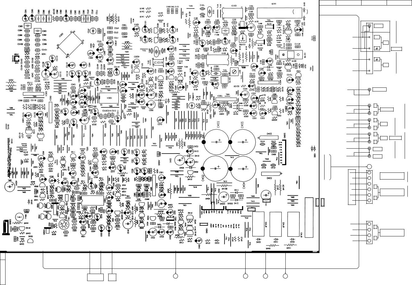
HCD-BX6AV/DX6AV
4-7. PRINTED WIRING BOARDS – MAIN Section – • See page 11 for Circuit Boards Location.
|
1 |
|
2 |
3 |
4 |
5 |
6 |
7 |
8 |
9 |
10 |
11 |
12 |
13 |
|
|
|
|
14 |
|
15 |
|
16 |
|
|
|
|
|
|
|
|
|
|
|
|
|
|
TP1 |
|
|
|
|
|
|
|
|
|
|
|
|
|
|
|
MAIN BOARD |
|
|
|
|
|
|
|
|
FOR |
|
|
|
|
|
|
|
|
|
|
|
|
|
|
|
|
|
|
|
|
|
|
|
ADJUSTMENT |
|
|
|
|
|
|
|
|
|
|
|
|
A |
|
|
|
|
|
|
|
|
|
|
|
|
|
|
|
|
|
|
|
|
(AEP, UK) |
|
|
|
|
|
|
|
|
|
|
|
|
|
|
|
|
|
|
|
|
|
|
|
|
FM 75Ω |
|
|
|
|
|
|
|
|
|
|
|
|
|
|
|
|
4 |
|
5 |
|
8 |
|
|
|
|
|
|
|
|
|
|
|
|
|
|
|
|
|
|
|
|
|
|
|
|
|
|
|
|
75Ω |
|
|
|
B |
|
|
|
|
|
|
|
|
|
|
|
|
|
|
|
|
|
|
|
|
|
FM |
|
|
|
|
|
|
|
|
|
|
|
|
|
|
|
|
|
|
|
|
|
|
|
|
JK101 |
|
|
|
|
|
|
|
|
|
|
|
|
|
|
|
|
|
|
|
|
|
|
|
|
|
|
|
|
|
|
|
|
|
|
|
|
|
|
|
|
|
|
|
|
|
|
|
|
|
|
ANTENNA |
|
|
|
|
|
|
|
|
|
|
|
|
|
|
|
|
|
|
|
|
|
|
(EXCEPT AEP, UK) |
|
||
C |
|
|
|
|
|
|
|
|
|
|
|
|
|
17 15 12 |
9 |
6 |
4 |
1 |
|
|
AM |
|
|
|
|
|
|
|
|
|
|
|
|
|
|
|
|
|
|
|
|
|
|||||||
|
|
|
|
|
|
|
|
|
|
|
|
|
18 |
13 |
10 |
7 |
|
2 |
|
|
|
|
|
|
|
|
|
C |
|
|
|
|
|
|
|
|
|
|
19 16 14 |
11 |
8 |
5 |
3 |
|
|
|
|
|
|
|
|
|
|
|
|
|
|
|
|
|
|
|
|
|
|
|
|
|
|
|
|
|
|
|
|
|
PANEL BOARD |
|
|
|
|
|
|
|
|
|
|
|
|
|
|
|
|
|
|
|
|
|
|
|
|
|
CN102 |
|
|
|
|
|
|
|
|
|
|
|
|
|
|
|
|
|
|
|
|
|
|
|
(Page 22) |
|
|
|
|
|
|
|
|
|
|
|
|
|
|
|
|
|
JK303 |
|
|
||
|
|
|
|
|
|
|
|
|
|
|
|
|
|
|
|
|
|
|
|
|
|
|
||
|
|
|
|
|
|
|
|
|
|
|
|
|
R130 |
|
|
|
|
BCE |
|
WOOFER OUT |
|
|
||
D |
|
|
|
|
|
|
|
|
|
|
|
|
|
|
|
|
|
|
|
|
|
|
|
|
|
|
|
|
|
|
|
|
|
|
|
|
|
1 |
|
|
|
|
|
|
|
|
|
|
|
|
|
|
|
|
|
|
|
|
|
|
|
|
|
|
|
|
|
|
|
|
|
|
|
|
|
|
|
|
|
|
|
|
|
|
|
|
|
|
|
|
|
|
|
|
|
R |
|
|
|
|
|
|
|
|
|
|
|
|
|
|
|
|
|
|
|
|
|
|
|
|
|
MD/VIDEO IN |
|
|
|
|
|
|
|
|
|
|
|
|
|
|
|
C356A |
|
|
|
|
|
|
|
L |
|
|
|
E |
|
|
|
|
|
|
|
|
|
|
|
|
|
|
|
|
|
|
|
|
|
|
|
|
|
|
|
|
|
|
|
|
|
|
|
|
|
|
|
|
|
|
|
|
R |
|
|
|
|
|
|
|
|
|
|
|
|
|
|
|
|
|
C355A |
|
|
|
|
|
|
|
|
FRONT |
|
|
|
|
|
|
|
|
|
|
|
|
|
|
|
|
|
|
|
|
|
|
|
L |
|
|
|
|
|
|
|
|
|
|
|
|
|
|
|
|
|
|
|
|
|
|
|
|
|
|
|
JK301 |
|
|
|
|
|
|
|
|
|
|
|
|
|
|
|
|
|
|
|
|
|
R |
|
|
|
|
|
|
|
|
|
|
|
|
|
|
|
|
|
|
|
|
|
|
|
|
|
REAR |
DVD INPUT |
|
F |
|
|
|
|
|
|
|
|
|
|
|
|
|
|
|
|
|
|
|
|
L |
|
|
|
|
|
|
|
|
|
|
|
|
|
|
|
|
|
|
|
|
|
|
|
|
|
|
|
|
|
|
|
|
|
|
|
|
|
|
|
|
|
|
|
|
|
|
|
|
|
WOOFER |
|
|
|
|
|
|
|
|
|
|
|
|
|
|
|
|
|
4 |
|
|
|
|
|
|
|
|
|
|
|
|
|
|
|
|
|
|
|
|
|
|
|
|
|
9 |
|
|
|
|
|
CENTER |
|
|
|
|
|
|
|
|
|
|
|
|
|
|
|
|
|
|
|
|
|
|
D002 |
H |
BACK UP |
(Page 24) |
|
|
G |
|
|
|
|
|
|
|
|
|
|
|
|
|
|
|
|
|
|
|
BOARD |
|
|||
|
|
|
|
|
|
|
|
|
|
|
|
|
|
|
|
|
|
|
+ |
CN502 |
|
|
|
|
|
|
D |
|
|
|
|
|
|
|
|
|
|
|
|
|
|
|
|
|
|
|
|
||
|
|
|
|
|
|
|
|
|
|
|
|
|
|
|
|
|
|
|
|
CENTER SPEAKER |
|
|||
|
|
|
|
|
|
|
|
|
|
|
|
|
|
|
|
|
|
|
|
– |
|
|
||
|
|
PANEL BOARD |
|
|
|
|
|
|
|
|
|
|
|
1 |
|
|
|
|
|
(IMPEDANCE USE 6-16Ω |
) |
|||
|
|
|
CN101 |
|
|
|
|
|
|
|
|
|
|
|
|
|
|
|
|
|
|
|
|
|
|
|
(Page 22) |
|
|
|
|
|
|
|
|
|
|
|
|
|
|
|
|
+ |
R |
|
|
JK402 |
|
|
|
|
|
|
|
|
|
|
|
|
|
|
|
1 |
|
|
|
|
|
– |
|
|
|
|
|
|
|
|
|
|
|
|
|
|
|
|
|
|
|
|
|
|
|
|
REAR SPEAKER |
|
|||
|
|
|
|
|
|
|
|
|
|
|
|
|
|
|
|
|
|
|
|
|
|
|||
|
|
|
|
|
|
|
|
|
|
|
|
|
|
|
|
|
|
|
|
|
|
|
||
H |
|
|
|
|
|
|
|
|
|
|
|
|
|
|
|
|
|
|
|
+ |
|
(IMPEDANCE USE 6-16Ω |
) |
|
|
|
|
|
|
|
|
|
|
|
|
|
|
|
|
|
|
|
|
L |
|
|
|
||
|
|
|
|
|
|
|
|
|
|
|
|
|
|
|
|
|
|
|
|
– |
|
|
|
|
|
|
|
|
|
|
|
|
|
|
|
|
|
|
|
|
|
|
|
|
|
|
|
|
|
|
H/P BOARD |
|
|
|
|
|
|
|
|
|
|
|
|
|
|
|
|
|
|
|
|
|
|
|
|
|
6 |
3 |
|
|
|
|
|
|
|
|
|
|
|
|
|
|
|
|
|
|
|
|
|
|
5 |
5 |
2 |
|
|
|
|
|
|
|
|
|
|
|
|
|
|
|
|
|
|
|
|
|
|
|
4 |
|
|
|
|
|
|
|
|
|
|
|
|
|
|
|
|
|
|
|
|
|
|
I |
1 |
|
1 |
|
|
|
|
|
|
|
|
|
|
|
|
|
|
|
|
|
|
|
|
|
|
|
|
|
|
|
|
|
|
|
|
|
|
|
|
|
|
|
+ |
|
|
|
|
||
|
|
|
|
|
|
|
|
|
|
|
|
|
|
|
|
|
|
|
|
R |
|
|
|
|
|
|
|
|
|
|
|
|
|
|
|
|
|
|
3 |
|
1 |
|
4 |
|
– |
|
JK401 |
|
|
|
|
|
|
|
|
|
|
|
|
|
|
|
|
|
|
|
|
|
|
|||||
|
|
|
|
|
|
|
|
|
|
|
|
|
|
|
|
|
|
|
|
|
||||
|
|
|
|
|
|
|
|
|
|
|
|
|
|
|
|
|
|
|
|
|
FRONT SPEAKER |
|
||
|
|
|
|
|
|
|
|
|
|
|
|
|
|
1 |
|
|
|
|
|
|
|
|
||
|
|
|
|
|
|
|
|
|
|
|
|
|
|
|
3 |
|
2 |
|
+ |
|
(IMPEDANCE USE 6-16Ω |
) |
||
|
|
|
|
|
|
|
|
|
|
|
|
|
|
|
|
|
|
|
|
L |
|
|
|
|
|
|
|
|
|
|
|
|
|
|
|
|
|
|
|
|
|
|
|
|
– |
|
|
|
|
|
|
|
|
|
|
|
|
|
|
|
|
|
|
|
|
|
|
|
|
|
|
|
|
|
J |
|
|
|
|
|
|
|
|
|
|
|
|
|
6 |
|
5 |
|
6 |
|
|
|
|
|
|
|
|
|
|
|
|
|
|
|
|
|
|
|
|
|
|
|
|
|
|
|
|
|||
K |
|
|
05 |
|
|
|
|
|
|
|
|
|
|
|
|
|
|
|
|
|
|
|
|
|
|
|
|
|
|
|
|
B |
|
|
E |
F |
G |
|
|
|
|
|
|
|
|
|
|
|
|
|
|
|
|
|
HRPE201 |
HP201 |
|
|
|
|
|
|
|
|
|
|
|
|
|
|
||||
|
|
|
|
|
(REC/PB/ERASE) |
(PB) |
|
DECORD BOARD |
|
|
CENTER/REAR |
FRONT |
CENTER/REAR |
|
|
|
|
|
|
|
|
|
|
|
|
|
|
|
|
|
|
|
|
|
|
|
|
|
|
|
|
|
|
|
|
||||
|
|
|
|
|
|
|
|
CN704 |
|
|
BOARD |
BOARD |
BOARD |
|
|
|
|
|
|
|
|
|
|
|
|
|
|
|
|
|
|
|
(Page 16) |
|
|
CN302 |
CN301 |
CN305 |
|
|
|
|
|
|
|
|
|
|
|
|
|
|
|
|
|
|
|
|
|
(Page 24) |
(Page 24) |
(Page 24) |
|
|
|
|
|
|
|
|
|
|
|
|
|
|
|
|
|
|
|
|
|
|
|
|
|
|
|
|
|
|
|
|
|
|
|||
|
|
|
|
|
|
|
|
|
17 |
17 |
|
|
|
|
|
|
|
|
|
|
|
|
|
|
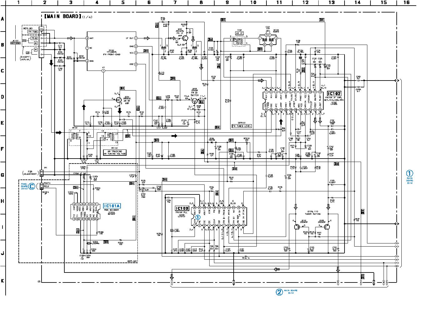
HCD-BX6AV/DX6AV
4-8. SCHEMATIC DIAGRAM – MAIN Section (1/4) – • See page 28 for Waveform. • See page 29 for IC Block Diagram.
(Page 19)
(Page 23)
• Voltages and waveforms are dc with respect to ground |
(Page 20) |
|
under no-signal (detuned) conditions. |
|
|
no mark : FM |
|
|
( |
) : AM |
|
18 18
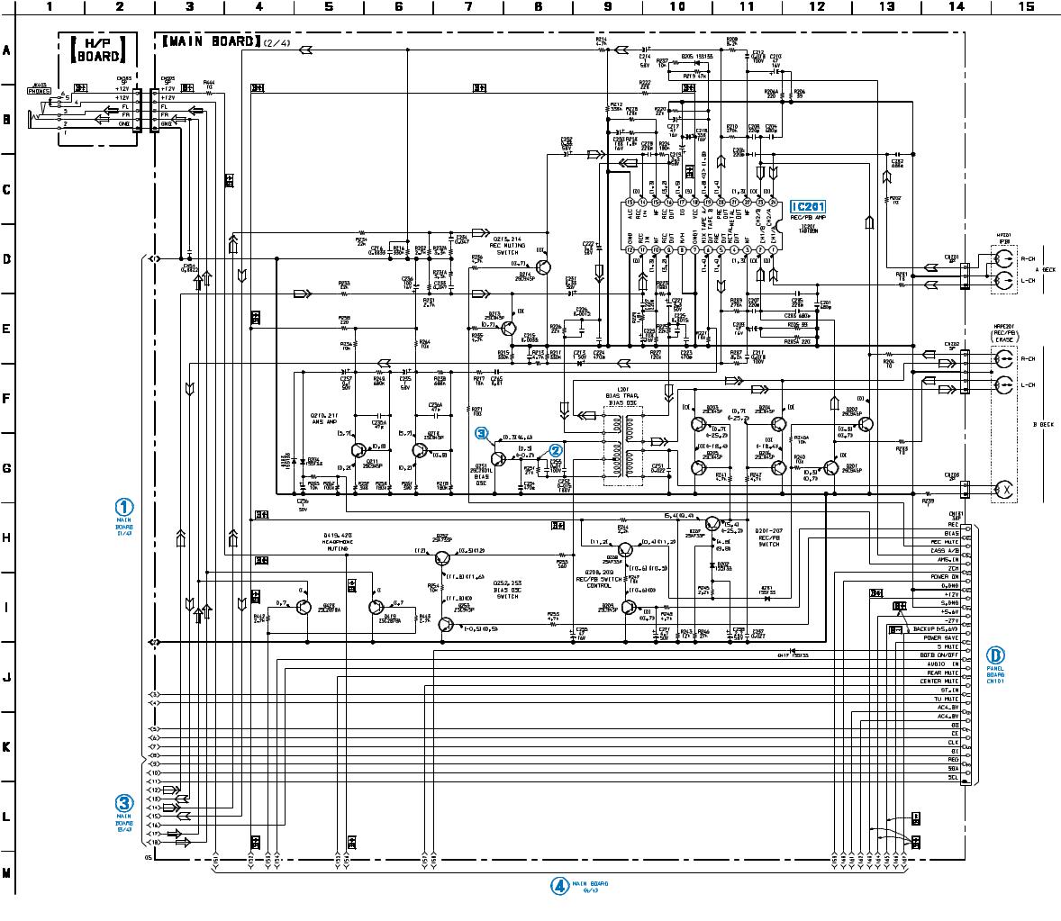
HCD-BX6AV/DX6AV
4-9. SCHEMATIC DIAGRAM – MAIN Section (2/4) – • See page 28 for Waveforms. • See page 29 for IC Block Diagram.
(Page 18)
(Page 20)
(Page 21)
19 19
(Page 23)
•Voltages and waveforms are dc with respect to ground under no-signal (detuned) conditions.
no mark : FM
[ ] : TAPE PLAY (DECK A)
< > : TAPE PLAY (DECK B)
: TAPE REC

HCD-BX6AV/DX6AV
4-10. SCHEMATIC DIAGRAM – MAIN Section (3/4) –
 (Page 18)
(Page 19)
(Page 13)
(Page 21)
•Voltages are dc with respect to ground under no-signal (detuned) conditions.
no mark : FM
20 20
Loading...