


Company Confidential
Copyright 2004© Siemens AG
Service Repair Documentation Level 2.5e – HIT – C65, CX65, M65
Release |
Date |
Department |
Notes to change |
1.0 |
01.06.2004 |
ICM MP CCQ GRM T |
New document |
|
|
|
|
|
|
|
|
Page 1 of 40 |
|
|
Service Repair Documentation |
Release 1.0 |
|
Level 2.5e – HIT – C65, CX65 and M65 |
||
|

Company Confidential
Copyright 2004© Siemens AG
Table of Contents:
1 |
List of available level 2,5e parts C65, CX65, M65 ........................................................ |
3 |
2 |
Required Equipment for Level 2,5e............................................................................... |
4 |
3 |
Required Software for Level 2,5e C65, CX65, M65 ...................................................... |
4 |
4 |
Radio Part..................................................................................................................... |
5 |
5 |
Logic / Control............................................................................................................. |
18 |
6 |
Power Supply.............................................................................................................. |
25 |
7 |
Camera ....................................................................................................................... |
28 |
8 |
Camera – Display Interface Module............................................................................ |
28 |
9 |
Display Modules.......................................................................................................... |
30 |
10 |
Illumination.................................................................................................................. |
32 |
11 |
Interfaces .................................................................................................................... |
34 |
12 |
Keyboard .................................................................................................................... |
40 |
Page 2 of 40 |
|
|
Service Repair Documentation |
Release 1.0 |
|
Level 2.5e – HIT – C65, CX65 and M65 |
||
|

Company Confidential
Copyright 2004© Siemens AG
1 List of available level 2,5e parts C65, CX65, M65
Component Typ/Circuit Part |
Mobile Phone |
Component Details |
ID |
Partnumber |
ASIC |
C65, M65 |
Camera Interface_S1D13716B02 |
D3601 |
L36820-U6054-D670 |
|
|
Power Supply D1094DA |
|
|
ASIC |
C65, CX65, M65 |
MOZART_TWIGO4 |
D1300 |
L36145-J4683-Y19 |
ASIC |
CX65 |
Camera Interface_S1D13716B01 |
D3601 |
L36820-U6052-D670 |
Cap_Diode_26MHz_Circuit |
C65, CX65, M65 |
Cap_Diode_1SV305 |
V3961 |
L36840-D61-D670 |
Capacitor_Camera_Circuit |
CX65, M65 |
Capacitor 2*2U2 |
C3609 |
L36344-F1225-M12 |
Capacitor_Mozart_Twigo_Circuit |
C65, CX65, M65 |
Capacitor 2*2U2 |
C1304 |
L36344-F1225-M12 |
Capacitor_Mozart_Twigo_Circuit |
C65, CX65, M65 |
Capacitor 2*2U2 |
C1315 |
L36344-F1225-M12 |
Capacitor_Mozart_Twigo_Circuit |
C65, CX65, M65 |
Capacitor 2*2U2 |
C1318 |
L36344-F1225-M12 |
Capacitor_Mozart_Twigo_Circuit |
C65, CX65, M65 |
Capacitor 2*2U2 |
C1329 |
L36344-F1225-M12 |
Capacitor_Mozart_Twigo_Circuit |
C65, CX65, M65 |
Capacitor 2*2U2 |
C1330 |
L36344-F1225-M12 |
Capacitor_Mozart_Twigo_Circuit |
C65 |
Capacitor 2*2U2 |
C1331 |
L36344-F1225-M12 |
Capacitor_Mozart_Twigo_Circuit |
C65, CX65, M65 |
Capacitor 2*2U2 |
C1332 |
L36344-F1225-M12 |
Coil_BATT+ |
C65, CX65, M65 |
Coil BKP1608HS391 |
L1300 |
L36140-F2100-Y6 |
Coil_BATT+ |
C65, CX65, M65 |
Coil BKP1608HS391 |
L1318 |
L36140-F2100-Y6 |
Coil_VBOOST |
C65, CX65, M65 |
Coil BKP1608HS391 |
L1331 |
L36140-F2100-Y6 |
Coil_VBOOST |
C65, CX65, M65 |
Coil 4U7 |
L1302 |
L36151-F5472-M1 |
Coil_VBUCK |
C65, CX65, M65 |
Coil 10U |
L1301 |
L36151-F5103-M3 |
Diode_Battery_Interface |
C65, CX65, M65 |
Diode BAV99T |
V1400 |
L36840-D66-D670 |
Diode_SIM_Circuit |
C65, CX65, M65 |
Diode ZENER EMZ6.8E |
V1605 |
L36840-D3088-D670 |
Diode_VBOOST |
C65, CX65, M65 |
Diode BAT760 |
V1303 |
L36840-D5076-D670 |
Diode_VBUCK |
C65, CX65, M65 |
Diode BAT760 |
V1302 |
L36840-D5076-D670 |
Diode_Vibra_Circuit |
CX65, M65 |
Diode BAV99T |
V2100 |
L36840-D66-D670 |
Filter_IO Interface |
C65, CX65, M65 |
EMI_EMV_Filter_IP4559CX25 |
Z1500 |
L36820-L6147-D670 |
IC MODUL PA |
C65, CX65, M65 |
PF08140B SMD |
N3981 |
L36851-Z2002-A63 |
IC_FEM |
C65, CX65, M65 |
FEM HITACHI GSM900 1800 1900 |
N3901 |
L36145-K280-Y258 |
IC_Processor_SGOLDLITELITE |
C65, CX65, M65 |
PMB8875 V1X |
D1000 |
L36810-G6191-D670 |
IC_Transceiver |
C65, CX65, M65 |
HD155155NPEB |
N3921 |
L36820-L6142-D670 |
Oszillator_RF_Logic |
C65, CX65, M65 |
Oszillator_26MHz |
Z3961 |
L36145-F260-Y17 |
Oszillator_RTC |
C65, CX65, M65 |
Oszillator_32,768KHZ |
Z1000 |
L36145-F102-Y21 |
Resistor_Temp_TVCXO |
C65, CX65, M65 |
Resistor_Temp 22k R |
R3967 |
L36120-F4223-H |
Switch_USB |
C65, CX65, M65 |
NC7WB66K8X DUAL BUS SWITCH |
N1501 |
L36810-B6132-D670 |
Trans_Charge_Circuit |
C65, CX65, M65 |
Transistor SI5933DC |
V1305 |
L36830-C1107-D670 |
Trans_DISPLAY_BACKLIGHT |
C65, CX65, M65 |
Transistor EMB9/PEMB9 |
V2303 |
L36840-C4059-D670 |
Trans_DISPLAY_BACKLIGHT |
C65 |
Transistor BC847BS BC846S |
V2302 |
L36840-C4061-D670 |
Trans_DISPLAY_BACKLIGHT |
C65, CX65 |
Transistor BC847BS/BC846S |
V2821 |
L36840-C4061-D670 |
Trans_DISPLAY_BACKLIGHT |
CX65, M65 |
Transistor BCS 46S |
V2302 |
L36840-C4014-D670 |
Trans_DISPLAY_BACKLIGHT |
M65 |
Transistor FDG6303N SI1902DL |
V2821 |
L36830-C1112-D670 |
Trans_NIGHT_DESIGN_LIGHT |
CX65, M65 |
Transistor FDG6303N SI1902DL |
V2404 |
L36830-C1112-D670 |
Trans_V2.65V |
C65, CX65, M65 |
Transistor EMD12 |
V1500 |
L36840-C4057-D670 |
Trans_VBOOST |
C65, CX65, M65 |
Transistor FDG313N |
V1304 |
L36830-C1121-D670 |
Volt.Regulator_Camera |
C65 |
Volt.Reg. LP3985ITLX-2.9 |
N3600 |
L36810-C6134-D670 |
Volt.Regulator_Camera |
CX65, M65 |
Volt.Reg. LP1986_2*2.85V |
N3600 |
L36810-C6065-D670 |
Page 3 of 40 |
|
|
Service Repair Documentation |
Release 1.0 |
|
Level 2.5e – HIT – C65, CX65 and M65 |
||
|

Company Confidential
Copyright 2004© Siemens AG
2 Required Equipment for Level 2,5e
-GSM-Tester (CMU200 or 4400S incl. Options)
-PC-incl. Monitor, Keyboard and Mouse
-Bootadapter 2000/2002 (L36880-N9241-A200)
-Adapter cable for Bootadapter due to new Lumberg connector (F30032-P226-A1)
-Troubleshooting Frame C65 (F30032-P377-A1)
-Troubleshooting Frame CX65, M65 (F30032-P343-A1)
-Power Supply (at least one GRT required power supply)
-Spectrum Analyser
-Active RF-Probe incl. Power Supply
-Oscilloscope incl. Probe
-RF-Connector (N<>SMA(f))
-Power Supply Cables
-Dongle (F30032-P28-A1) if USB-Dongle is used a special driver for NT is required
-BGA Soldering equipment
Reference: Equipment recommendation Version X (newest version) (downloadable from the technical support page)
3 Required Software for Level 2,5e C65, CX65, M65
-Winsui for 65series
-Software for GSM-Tester (GRT)
-Software for reference oscillator adjustment
-Internet unblocking solution (JPICS)
-Dongle driver for dongle protected Siemens software tools
Page 4 of 40 |
|
|
Service Repair Documentation |
Release 1.0 |
|
Level 2.5e – HIT – C65, CX65 and M65 |
||
|

Company Confidential
Copyright 2004© Siemens AG
4 Radio Part
The radio part realizes the conversion of the GMSK-HF-signals from the antenna to the base-band and vice versa.
In the receiving direction, the signals are split in the I- and Q-component and led to the D/A- converter of the logic part. In the transmission direction, the GMSK-signal is generated in an Up Conversion Modulation Phase Locked Loop by modulation of the I- and Q-signals which were generated in the logic part. After that the signals are amplified in the power amplifier.
Transmitter and Receiver are never active at the same time. Simultaneous receiving in two bands is impossible. Simultaneous transmission in two bands is impossible, too. However the monitoring band (monitoring timeslot) in the TDMA-frame can be chosen independently of the receiving respectively the transmitting band (RXand TX timeslot of the band).
The RF-part of the C65, CX65 and M65 are dimensioned for triple band operation (EGSM900, GSM1800, GSM1900) supporting GPRS functionality up to multiclass 10.
The RF-circuit consists of the following components:
•Hitachi Bright VE chip set with the following functionality: o PLL for local oscillator LO1 and LO2 and TxVCO
o Integrated local oscillators LO1, LO2 (without loop filter)
o Integrated TxVCO (without loop filter and core inductors for GSM)
o Direct conversion receiver including LNA, DC-mixer, channel filtering and PGCamplifier
o Active part of 26 MHz reference oscillator
•Hitachi LTCC transmitter power amplifier with integrated power control circuitry
•Hitachi Frontend-Module including RX-/TX-switch and EGSM900 / GSM1800 / GSM 1900 receiver SAW-filters
Quartz and passive circuitry of the 26MHz VCXO reference oscillator.
Page 5 of 40 |
|
|
Service Repair Documentation |
Release 1.0 |
|
Level 2.5e – HIT – C65, CX65 and M65 |
||
|

Company Confidential
Copyright 2004© Siemens AG
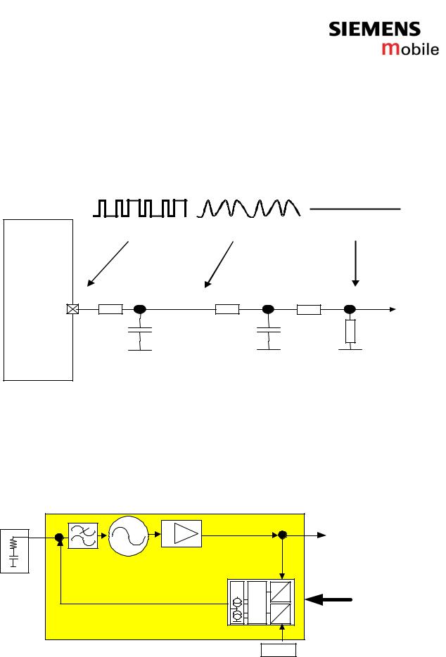
4.1 Block diagram RF part
65er Serie
internal antenna
antenna
Page 6 of 40 |
|
|
Service Repair Documentation |
Release 1.0 |
|
Level 2.5e – HIT – C65, CX65 and M65 |
||
|
Company Confidential
Copyright 2004© Siemens AG
4.2 Power Supply RF-Part
The voltage regulator for the RF-part is located inside the ASIC D1300.(see chapter 5.2).It generates the required 2,85V “RF-Voltage” named VDD_RF1(VDD_BRIGHT). The voltage regulator is activated as well as deactivated via VCXOEN_UC (Functional F23) provided by the SGOLDLITE+. The temporary deactivation is used to extend the stand by time.
Circuit diagram
VDD_RF1
4.3 Frequency generation
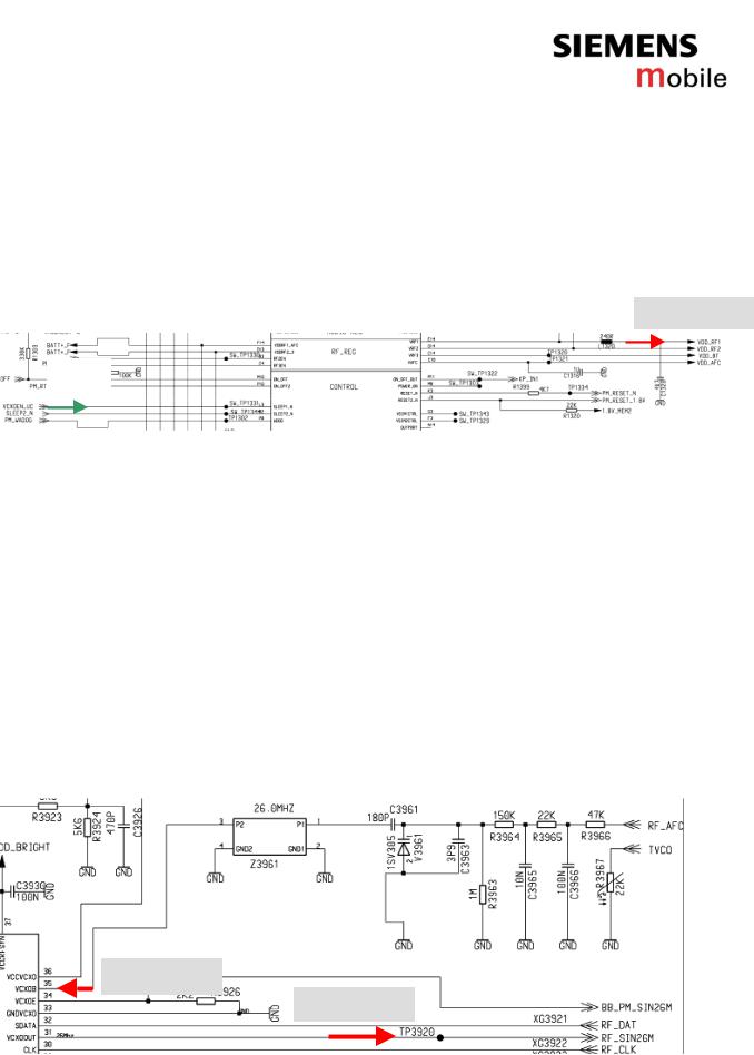
4.3.1 Synthesizer: The discrete VCXO (26MHz)
The C65, CX65 and M65 mobile is using a reference frequency of 26MHz. The generation of the 26MHz signal is done via a VCXO. This oscillator consists mainly of:
A 26MHz VCXO |
Z3961 |
A capacity diode |
V3961 |
TP (test point) of the 26MHz signal is the TP 3920
The oscillator output signal 26MHz_RF is directly connected to the BRIGHT IC (pin 35) to be used as reference frequency inside the Bright (PLL). The signal leaves the Bright IC as RF_SIN26M (pin 31) to be further used from the SGOLDLITE+ (D171 (Functional AE15)).
Bright In
SGOLDLIT
Page 7 of 40 |
|
|
Service Repair Documentation |
Release 1.0 |
|
Level 2.5e – HIT – C65, CX65 and M65 |
||
|
Company Confidential
Copyright 2004© Siemens AG
To compensate frequency drifts (e.g. caused by temperature) the oscillator frequency is controlled by a (RF_AFC) signal, generated through the internal SGOLDLITE+ (D171 (Functional A9)) PLL via the capacity diode V3961. Reference for the “SGOLDLITE-PLL” is the base station frequency received via the Frequency Correction Burst. To compensate a temperature caused frequency drift, the temperature-depending resistor R3967 is placed near the VCXO to measure the temperature. The measurement result TVCXO is reported to the SGOLDLITE+(Analog Interface M25) via R3967.
Waveform of the AFC_PNM signal from SGOLDLITE+ to Oscillator
Signalform
SGOLDLITE+
1 |
2 |
3 |
1 |
R3966 |
AFC_PNM |
2 |
R3965 |
R3964 |
3 |
AFC |
|
|
|
|||
|
|
|
|
|
|
|
|
|
C3966 |
|
|
C3965 |
R3963 |
|
|
|
|
|
|
|
|
|
GND |
|
|
GND |
GND |
4.3.2 Synthesizer: RFVCO(LO1)
The first local oscillator (LO1) consists of a PLL and VCO inside Bright (N3921) and an external loop filter The first local oscillator is needed to generate frequencies which enable the transceiver IC to demodulate the receiver signal and to perform the channel selection in the TX part. To do so, a control voltage for the LO1 is used, gained by a comparator. This control voltage is a result of the comparison of the divided LO1 and the 26MHz reference
Signal. The division ratio of the dividers is programmed by the SGOLDLITE+, according to the network channel requirements.
|
|
|
|
|
|
RF VCO |
|
|
|
|
|
|
OUT |
|
3476 - 3980 |
|
|
|
|
|
external |
MHz |
RF PLL |
CP |
PFD |
D |
|
|
|
|||||
Loopfilter |
|
|
+ |
|
1 |
|
|
|
|
|
R |
3 wire bus |
|
|
|
|
|
|
||
|
Bright V |
|
|
|
1 |
from EGOLD |
|
|
|
|
|
||
|
|
|
|
|
26MHz |
|
Page 8 of 40 |
|
|
Service Repair Documentation |
Release 1.0 |
|
Level 2.5e – HIT – C65, CX65 and M65 |
||
|
Company Confidential
Copyright 2004© Siemens AG
Matrix to calculate the TX and RX frequencies
Band |
RX / TX |
Channels |
RF frequencies |
LO1 frequency |
IF freq. |
EGSM 900 |
Receive: |
0..124 |
935,0 - 959,8 MHz |
LO1 = 4*RF |
|
EGSM 900 |
Transmit: |
0..124 |
890,0 - 914,8 MHz |
LO1 = 4*(RF+IF) |
80,0 MHz |
EGSM 900 |
Receive: |
975..1023 |
925,2 - 934,8 MHz |
LO1 = 4*RF |
|
EGSM 900 |
Transmit: |
975..1023 |
880,2 - 889,8 MHz |
LO1 = 4*(RF+IF) |
82,0 MHz |
GSM 1800 |
Receive: |
512..661 |
1805,2 - 1835,0 MHz |
LO1 = 2*RF |
|
GSM 1800 |
Transmit: |
512..661 |
1710,2 - 1740,0 MHz |
LO1 = 2*(RF+IF) |
80,0 MHz |
GSM 1800 |
Receive: |
661..885 |
1835,0 - 1879,8 MHz |
LO1 = 2*RF |
|
GSM 1800 |
Transmit: |
661..885 |
1740,0 - 1784,8 MHz |
LO1 = 2*(RF+IF) |
82,0 MHz |
GSM 1900 |
Receive: |
512..810 |
1930,2 - 1989,8 MHz |
LO1 = 2*RF |
|
GSM 1900 |
Transmit: |
512..810 |
1850,2 - 1909,8 MHz |
LO1 = 2*(RF+IF) |
80,0 MHz |
4.3.3 Synthesizer: IFVCO(LO2)
The second local oscillator (LO2) consists of a PLL and a VCO which are integrated in Bright and a second order loopfilter which is realized external (R3927; C3940; C3948). Due to the direct conversion receiver architecture, the LO2 is only used for transmit-operation.
The LO2 covers a frequency range of at least 16 MHz (640MHz – 656MHz).
Before the LO2-signal gets to the modulator it is divided by 8. So the resulting TX-IF frequencies are 80/82 MHz (dependent on the channel and band). The LO2 PLL and powerup of the VCO is controlled via the tree-wire-bus of Bright (SGOLDLITE+ signals RFDATA;
RFCLK; RFSTR). To ensure the frequency stability, the 640MHz VCO signal is compared by the phase detector of the 2nd PLL with the 26Mhz reference signal. The resulting control signal passes the external loop filter and is used to control the 640/656MHz VCO.
|
|
|
|
|
IF VCO |
|
|
|
|
|
OUT |
|
640 - 656 MHz |
|
|
|
|
external |
IF PLL |
CP |
PFD |
D |
|
Loopfilter |
|
+ |
|
1 |
|
|
|
|
R |
3 wire bus |
|
|
|
|
|
||
|
Bright V |
|
|
1 |
from EGOLD |
|
|
|
|
||
|
|
|
|
26MHz |
|
Page 9 of 40
Service Repair Documentation |
Release 1.0 |
|
Level 2.5e – HIT – C65, CX65 and M65 |
||
|
Company Confidential
Copyright 2004© Siemens AG
4.3.4 Synthesizer: PLL
The frequency-step is 400 kHz in GSM1800/GSM1900 mode and 800kHz in EGSM900 mode due to the internal divider by two for GSM1800/GSM19000 and divider by four for EGSM900. To achieve the required settling-time in GPRS operation, the PLL can operate in fastlock-mode a certain period after programming to ensure a fast settling. After this the loopfilter and currents are switched into normal-mode to get the necessary phasenoiseperformance. The PLL is controlled via the tree-wire-bus of Bright.
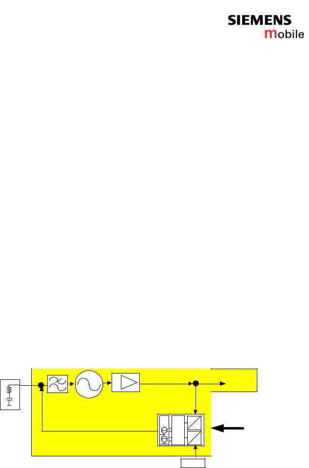
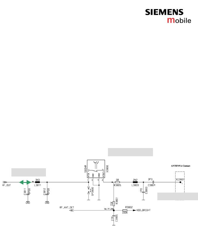
4.4 Antenna switch (electrical/mechanical)
Internal/External <> Receiver/Transmitter
The mobile have two antenna switches.
a)The mechanical antenna switch for the differentiation between the internal and external antenna, which is used only RF adjustment.
b)The electrical antenna switch, for the differentiation between the receiving and transmitting signals.
To activate the correct settings of this diplexer, the SGOLDLITE+ signals RF_SW and TXON_GSM are required
External Antenna
to / from FEM
ntenna
Internal antenna
Page 10 of 40 |
|
|
Service Repair Documentation |
Release 1.0 |
|
Level 2.5e – HIT – C65, CX65 and M65 |
||
|

Company Confidential
Copyright 2004© Siemens AG
The electrical antenna switch
N3901:
Top View
Switching Matrix |
Pin assignment |
Page 11 of 40
Service Repair Documentation
Level 2.5e – HIT – C65, CX65 and M65
Bright
Release 1.0
Company Confidential
Copyright 2004© Siemens AG
4.5 Receiver
Receiver: Filter to Demodulator
The band filters are located inside the frontend module (N3901). The filters are centred to the band frequencies. The symmetrical filter output is matched to the LNA input of the Bright
(N3921).The Bright VE incorporates three RF LNAs for GSM850/EGSM900, GSM1800 and GSM1900 operation. The LNA/mixer can be switched in Highand Low-mode to perform an amplification of ~ 20dB. For the “High Gain“ state the mixers are optimised to conversion gain and noise figure, in the “Low Gain“ state the mixers are optimised to large-signal behaviour for operation at a high input level. The Bright performs a direct conversion mixers which are IQ-demodulators. For the demodulation of the received GSM signals the LO1 is required. The channel depending LO1 frequencies for 1800MHz/1900MHz bands are divided by 2 and by 4 for 850MHG/900MHz band. Furthermore the IC includes a programmable gain baseband amplifier PGA (90 dB range, 2dB steps) with automatic DCoffset calibration. LNA and PGA are controlled via SGOLDLITE+ signals RFDATA; RFCLK; RFSTR(RF_Ctrl C8, B10, B12). The channel-filtering is realized inside the chip with a three stage baseband filter for both IQ chains. Only two capacitors which are part of the first passive RC-filters are external. The second and third filters are active filters and are fully integrated.
The IQ receive signals are fed into the A/D converters in the EGAIM part of SGOLDLITE+.
The post-switched logic measures the level of the demodulated baseband signal and regulates the level to a defined value by varying the PGA amplification and switching the appropriate LNA gains.
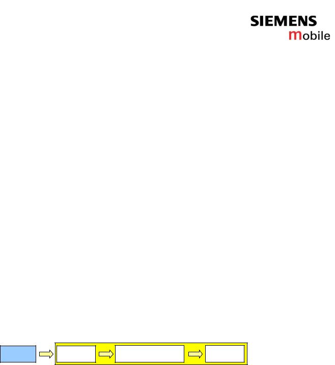
From the antenna switch, up to the demodulator the received signal passes the following blocks to get the demodulated baseband signals for the SGOLDLITE+:
Filter |
LNA |
Demodulator |
PGC |
N3901 |
|
Bright(N3921) |
|
Page 12 of 40 |
|
|
Service Repair Documentation |
Release 1.0 |
|
Level 2.5e – HIT – C65, CX65 and M65 |
||
|
 Loading...