


Samsung VCP-007LR, SVR-140, SVR-141, SVR-2401, SVR-240W Service Manual
...ELECTRONICS
© Samsung Electronics Co., Ltd. MAR. 2001
Printed in Korea
AC68-01530A
MANUAL SERVICE
007LR-443/440/243/240B/240W/2401/141/140/VCP-SVR
VIDEO CASSETTE RECORDER
Chassis : Scorpio
SVR-443/440
SVR-243/240B/240W/2401
SVR-141/140
VCP-007LR
SERVICE Manual 
For mechanical disassembly and adjustment, refer to the “Mechanical Manual” (TS-10  AC68-01405A).
VIDEO CASSETTE RECORDER |
|
CONTENTS |
1. Precautions
|
STANDBY/ON |
|
|
REW |
F.F |
EJECT |
|
|
|
||
|
|
|
|
|
|
VIDEO |
AUDIO |
PROG |
REC |
STOP PLAY |
|
|
|
LINE IN 2 |
|
|
|
SVR-443/243
POWER |
|
|
|
EJECT |
|
|
|
|
|
REW |
PLAY |
|
|
F.F |
|
CHANNEL |
REC |
STOP |
|
SVR-440/240B/240W
2.Alignment and Adjustment
3.Exploded View and Parts List
4.Electrical Parts List
5.Schematic Diagrams
PLAY
STANDBY/ON |
|
PROG |
REC STOP |
SVR-2401/VCP-007LR |
|
EJECT STANDBY/ON |
REW |
|
|
PROG |
REC |
STOP |
PLAY |
SVR-141
EJECT STANDBY/ON
REW PLAY F.F
PROG |
REC STOP |
SVR-140
IMPORTANT SERVICE GUIDE
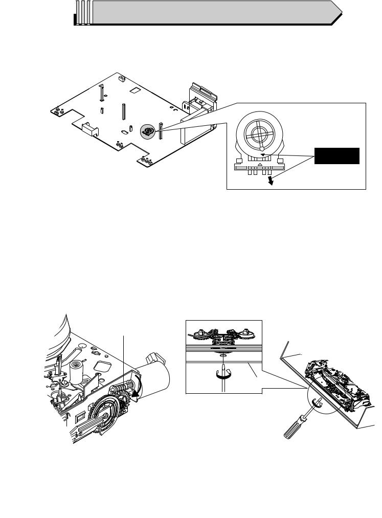
MODE SWITCH (PROGRAM SWITCH) ASSEMBLY POINT
1) When installing the ass’y deck on the Main PCB, be sure to align the assembly point of mode switch.
ASSEMBLY POINT (ALIGN TWO ARROWS)
Fig. 1
HOW TO EJECT THE CASSETTE TAPE
(If the unit does not operate on condition that tape is inserted into housing ass’y)
1)Turn the Gear Worm Œ clockwise in the direction of arrow with screw driver. (See Fig. 2) (Other method ; Remove the screw of Motor Load Ass’y, Separate the Motor Load Ass’y)
2)When Slider S, T are approached in the position of unloading, rotate holder Clutch counterclockwise after inserting screw driver in the hole of frame’s bottom in order to wind the unwiunded tape. (Refer to Fig. 3)
(If you rotate Gear Worm Πcontinuously when tape is in state of unwinding, you may cause a tape contamination by grease and tape damage. Be sure to wind the unwiunded tape in the state of set horizontally.)
3)Rotate Gear Worm ˇ clockwise using screw driver again up to the state of eject mode and then pick out the tape. (Refer to Fig. 2)
ΠGEAR WORM
FRAME
Fig. 3

1. Precautions
1.Be sure that all of the built-in protective devices are replaced. Restore any missing protective shields.
2.When reinstalling the chassis and its assemblies, be sure to restore all protective devices, including : control knobs and compartment covers.
3.Make sure that there are no cabinet openings through which people--particularly children --might insert fingers and contact dangerous voltages. Such openings include the spacing between the picture tube and the cabinet mask, excessively wide cabinet ventilation slots, and improperly fitted back covers.
If the measured resistance is less than 1.0 megohm or greater than 5.2 megohms, an abnormality exists that must be corrected before the unit is returned to the customer.
4.Leakage Current Hot Check (See Fig. 1-1) : Warning : Do not use an isolation transformer during this test. Use a leakage current tester or a metering system that complies with American National Standards Institute (ANSI C101.1, Leakage Current for Appliances), and Underwriters Laboratories (UL Publication UL1410, 59.7).
5.With the unit completely reassembled, plug the AC line cord directly the power outlet. With the unit’s AC switch first in the ON position and then OFF, measure the current between a known earth ground (metal water pipe, conduit, etc.) and all exposed metal parts, including : antennas, handle brackets, metal cabinets, screwheads and control shafts. The current measured should not exceed 0.5 milliamp. Reverse the power-plug prongs in the AC outlet and repeat the test.
6.X-ray Limits :
The picture tube is designed to prohibit X-ray emissions. To ensure continued X-ray protection, replace the picture tube only with one that is the same type as the original.
|
|
|
|
|
|
|
|
|
(READING SHOULD |
||
|
|
|
|
|
|
|
|
|
|
|
NOT BE ABOVE |
|
|
|
|
|
|
|
|
|
|
|
0.5mA) |
DEVICE |
LEAKAGE |
||||||||||
CURRENT |
|||||||||||
UNDER |
|
TESTER |
|||||||||
TEST |
|
|
|
|
|
|
|
|
|
|
|
|
TEST ALL |
|
|
|
|
|
|
|
|
||
|
|
|
|
|
|
|
|
|
|
||
|
|
|
|
|
|
|
|
|
|
||
|
EXPOSED METER |
|
|
|
|
|
|
|
|
||
|
|
SURFACES |
|
|
|
|
|
|
|
|
|
2-WIRE CORD |
|
|
|
|
|
|
|
|
|||
|
|
|
|
|
|
|
|
||||
ALSO TEST WITH |
|
|
|
|
|
|
|
EARTH |
|||
|
|
|
|
|
|
|
|||||
|
|
|
|
|
|
|
|||||
PLUG REVERSED |
|
|
|
|
|
|
|
||||
|
|
|
|
|
|
|
GROUND |
||||
|
|
|
|
|
|
|
|||||
(USING AC ADAPTER |
|
|
|
|
|
|
|
||||
|
|
|
|
|
|
|
|
||||
PLUG AS REQUIRED) |
|
|
|
|
|
|
|
|
|||
Fig. 1-1 AC Leakage Test
7. Antenna Cold Check :
With the unit’s AC plug disconnected from the AC source, connect an electrical jumper across the two AC prongs. Connect one lead of the ohmmeter to an AC prong.
Connect the other lead to the coaxial connector.
8.High Voltage Limit :
High voltage must be measured each time servicing is done on the B+, horizontal deflection or high voltage circuits.
Heed the high voltage limits. These include the X-ray protection Specifications Label, and the Product Safety and X-ray Warning Note on the service data schematic.
9.Some semiconductor (“solid state”) devices are easily damaged by static electricity.
Such components are called Electrostatically Sensitive Devices (ESDs); examples include integrated circuits and some field-effect transistors. The following techniques will reduce the occurrence of component damage caused by static electricity.
10.Immediately before handling any semiconductor components or assemblies, drain the electrostatic charge from your body by touching a known earth ground. Alternatively, wear a discharging Wrist-strap device. (Be sure to remove it prior to applying power--this is an electric shock precaution.)
Samsung Electronics |
1-1 |

Precautions
11.High voltage is maintained within specified limits by close-tolerance, safety-related components and adjustments. If the high voltage exceeds the specified limits, check each of the special components.
12.Design Alteration Warning :
Never alter or add to the mechanical or electrical design of this unit. Example : Do not add auxiliary audio or video connectors.
Such alterations might create a safety hazard. Also, any design changes or additions will void the manufacturer’s warranty.
13. Hot Chassis Warning :
Some TV receiver chassis are electrically connected directly to one conductor of the AC power cord. If an isolation transformer is not used, these units may be safely serviced only if the AC power plug is inserted so that the chassis is connected to the ground side of the AC source.
To confirm that the AC power plug is inserted correctly, do the following : Using an AC voltmeter, measure the voltage between the chassis and a known earth ground. If the reading is greater than 1.0V, remove the AC power plug, reverse its polarity and reinsert. Re-measure the voltage between the chassis and ground.
14.Some TV chassis are designed to operate with 85 volts AC between chassis and ground, regardless of the AC plug polarity. These units can be safely serviced only if an isolation transformer inserted between the receiver and the power source.
15.Never defeat any of the B+ voltage interlocks. Do not apply AC power to the unit (or any of its assemblies) unless all solid-state heat sinks are correctly installed.
16.Always connect a test instrument’s ground lead to the instrument chassis ground before connecting the positive lead; always remove the instrument’s ground lead last.
17.Observe the original lead dress, especially near the following areas : Antenna wiring, sharp edges, and especially the AC and high voltage power supplies. Always inspect for pinched, out- of-place, or frayed wiring. Do not change the spacing between components and the printed circuit board. Check the AC power cord for damage. Make sure that leads and components do not touch thermally hot parts.
18. Picture Tube Implosion Warning :
The picture tube in this receiver employs “integral implosion” protection. To ensure continued implosion protection, make sure that the replacement picture tube is the same as the original.
19.Do not remove, install or handle the picture tube without first putting on shatterproof goggles equipped with side shields. Never handle the picture tube by its neck. Some “in-line” picture tubes are equipped with a permanently attached deflection yoke; do not try to remove such “permanently attached” yokes from the picture tube.
20.Product Safety Notice :
Some electrical and mechanical parts have special safety-related characteristics which might not be obvious from visual inspection. These safety features and the protection they give might be lost if the replacement component differs from the original--even if the replacement is rated for higher voltage, wattage, etc.
Components that are critical for safety are indicated in the circuit diagram by shading, (  or
or  ).
).
Use replacement components that have the same ratings, especially for flame resistance and dielectric strength specifications. A replacement part that does not have the same safety characteristics as the original might create shock, fire or other hazards.
1-2 |
Samsung Electronics |
2. Alignment and Adjustment
2-1 Reference
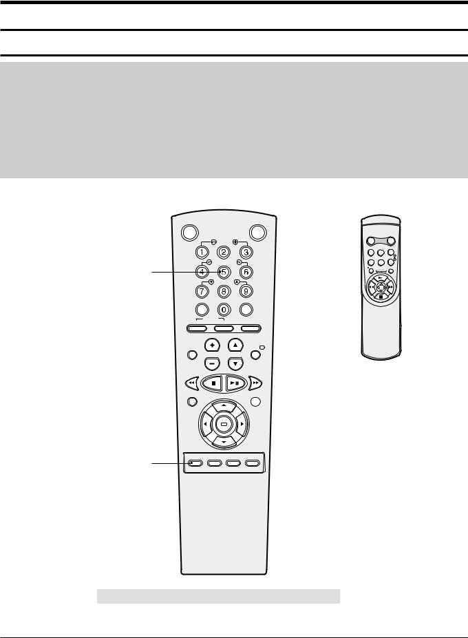
1)X-Point (Tracking center) adjustment, “Head switching adjustment” and “NVRAM option setting” can be adjusted with remote control.
2)When replacing the Micom (IC601) and NVRAM (IC605 ; EEPROM) be sure to adjust the “Head switching adjustment” and “NVRAM option setting”.
3)When replacing the cylinder ass’y, be sure to adjust the “X-Point” and “Head switching adjustment”.
4)Among Samsung VCR remote control used for adjustment as a accessory, only the remote control that has figures buttons (0 ~ 9) is available for all adjustment regardless of chassis.
5)How to adjustment.
-Press the “SW718” button on Main PCB to set the adjustment mode.
-If the corresponding adjustment button is pressed, the adjustment is performed automatically.
-If the adjustment is completed, be sure to turn the power off.
2-1-1 Location of adjustment button of remote control
X-Point (Tracking Center) Adjustment
("5" Button)
Head Switching Adjustment
("SPEED" Button)
VCR STANDBY/ON |
|
TV STANDBY/ON |
|
|
|
|
STANDBY/ON |
|
DISPLAY |
|
SLOW |
|
|
|
|
|
CNT.RESET SPEED |
|
|
SHUTTLE |
IIP/S IPC |
|
TRK |
|
|
|
|
||
|
|
REC |
E |
MENU |
|
|
REP |
AT |
|
V-LOCK |
|
|
|
|
CLR/RST |
F.ADV |
INDEX |
|
|
-/-- |
|
|
|
|
SELECT |
INPUT |
|
|
|
TV |
VCR |
|
|
|
|
|
REPEAT |
|
|
AUDIO |
|
DISP./ |
|
|
VOL |
PROG/TRK |
|
|
|
|
|
<This type of remote |
|
can not adjust.> |
REC |
|
MENU |
|
|
 NVRAM Option Setting
("MENU" Button)
OK
SPEED DUB TV/VCR TIMER
<This type of remote control can adjust.>
Remote Control for adjustment is not supplied as a Service Jig.
Fig. 2-1
Samsung Electronics |
2-1 |

Alignment and Adjustment
2-1-2 SW718 (TEST) location for adjustment mode setting
PRESS
Fig. 2-2 Main PCB (Top View)
2-2 |
Samsung Electronics |
Alignment and Adjustment
2-2 Mechanical Adjustment
Note : Refer to the Mechanical Manual “TS-10 (AC68-01405A)” for the adjustment and confirmation of ass’y full deck.
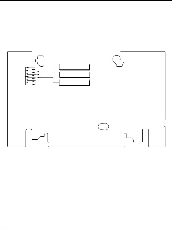
2-2-1 The number and position of test point
|
Test point : |
TP601 (Control pulse) |
TP301 (Envelope) |
|
|
|
|
||||
|
|
TP602 (H’D S/W -Trigger) |
TP302 (Audio output) |
|
|
|
|
|
|
TP303 (Video output) |
|
|
|
|
|
|
|
|
|
|
|
|
|
AUDIO OUTPUT
ENVELOPE
HEAD SWITCHING
Fig. 2-3 Location of Test point (Main PCB-Top View)
2-2-2 ACE Head Position (X-Point) Adjustment
(See the 2-2-1(d) ACE Head Position (X-Point) Adjustment on page 2-2 of the Mechanical Manual)
1)Playback the alignment tape (Color bar).
2)Press the “SW718” button on Main PCB to set the adjustment mode. (See Fig. 2-2)
3)Press the “5” button of remote control then adjustment is operated automatically. (See Fig. 2-1)
4)Connect the CH-1 probe to TP301 (Envelope) the CH-2 probe to TP602 (H’D switching pulse) and then trigger to CH-1.
5)Insert the (-) driver into the X-Point adjustment hole and adjust it so that envelope waveform is maximum.
6)Turn the Power off.
Samsung Electronics |
2-3 |
Alignment and Adjustment
2-3 Head Switching Point Adjustment
1)Playback the alignment tape.
2)Press the “SW718” button on Main PCB to set the adjustment mode. (See Fig. 2-2)
3)Press the “SPEED” button of remote control then adjustment is operated automatically. (See Fig. 2-1)
4)Turn the Power off.
2-4 NVRAM Option Setting
1)NVRAM Option is adjusted at production line basically.
2)In case Micom (IC601) and NVRAM (IC605 ; EEPROM) is replaced, be sure to set the corresponding option number of the repaired model. (If the option is not set, the unit is not operated.)
1)Press the “SW718” button on Main PCB to set the adjustment mode. (See Fig. 2-2)
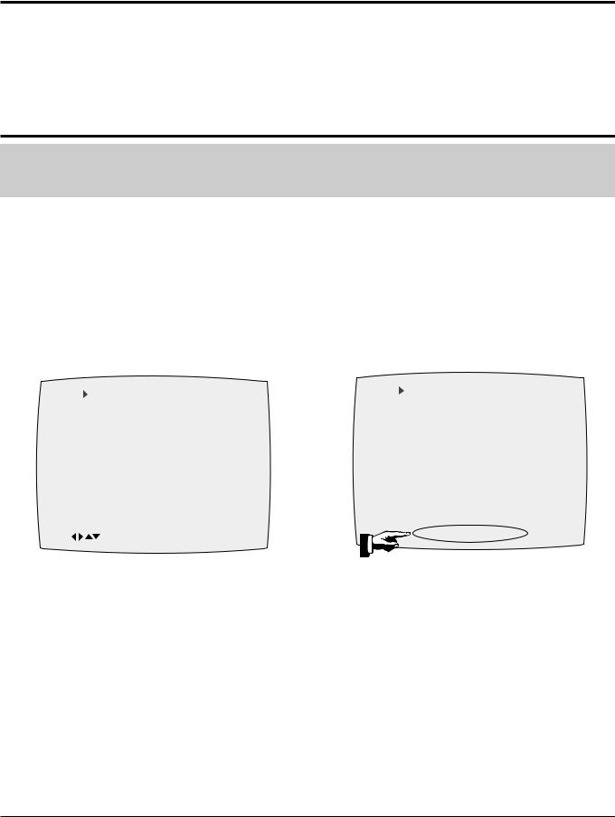
2)Press the “MENU” button on the remote control about 5 seconds then option setting display is appeared. (See Fig. 2-4)
3)Select the option number (See Table 2-1) of corresponding model with “CURSOR” button on the remote control.
4)If selecting the option number is completed, press the “OK” button of remote control. (If “OK” button is pressed, the selected number is changes reversed color. ; See Fig. 2-4)
5)Press the “MENU” button of remote control again to store the option number.
(“PLEASE WAIT” is displayed for a second as shown Fig. 2-5 and this setting is completed.)
6)Turn the Power off.
01 |
|
03 |
04 |
|
06 |
07 |
08 |
01 |
02 |
03 |
04 |
05 |
06 |
07 |
08 |
|
02 |
05 |
|||||||||||||||
|
|
|||||||||||||||
09 |
10 |
11 |
12 |
13 |
14 |
15 |
16 |
09 |
10 |
11 |
12 |
13 |
14 |
15 |
16 |
|
17 |
18 |
19 |
20 |
21 |
22 |
23 |
24 |
17 |
18 |
19 |
20 |
21 |
22 |
23 |
24 |
|
25 |
26 |
27 |
28 |
29 |
30 |
31 |
32 |
25 |
26 |
27 |
28 |
29 |
30 |
31 |
32 |
|
33 |
34 |
35 |
36 |
37 |
38 |
39 |
40 |
33 |
34 |
35 |
36 |
37 |
38 |
39 |
40 |
|
41 |
42 |
43 |
44 |
45 |
46 |
47 |
48 |
41 |
42 |
43 |
44 |
45 |
46 |
47 |
48 |
|
49 |
50 |
51 |
52 |
53 |
54 |
55 |
56 |
49 |
50 |
51 |
52 |
53 |
54 |
55 |
56 |
|
57 |
58 |
59 |
60 |
61 |
62 |
63 |
64 |
57 |
58 |
59 |
60 |
61 |
62 |
63 |
64 |
|
65 |
66 |
67 |
68 |
69 |
70 |
71 |
72 |
65 |
66 |
67 |
68 |
69 |
70 |
71 |
72 |
|
CNG : OK SAVE : MENU |
PLEASE WAIT |
|
Fig. 2-4 |
Fig. 2-5 |
|
<Table 2-1 NVRAM Option Number> |
|
|
|
|
MODELS |
OPTION NUMBER |
|
SVR-443 |
9, 10, 15, 20, 24, 30, 32, 34, 36, 38, 42, 44, 47, 54, 57, 60, 61, 63 |
|
SVR-440 |
9, 10, 20, 30, 32, 34, 36, 38, 42, 44, 47, 52, 54, 57, 60, 61, 63 |
|
SVR-243 |
10, 15, 20, 24, 30, 32, 34, 36, 37, 42, 44, 47, 54, 57, 60, 61, 63, 71 |
|
SVR-240B |
10, 20, 30, 32, 34, 36, 37, 42, 44, 47, 52, 54, 57, 60, 61, 63, 71 |
|
SVR-240W |
10, 20, 30, 32, 34, 36, 37, 42, 44, 47, 52, 54, 57, 60, 61, 63, 71 |
|
SVR-2401 |
10, 20, 30, 34, 36, 37, 42, 44, 47, 52, 54, 57, 60, 61, 63, 71 |
|
SVR-141 |
10, 20, 24, 35, 37, 42, 44, 51, 54, 57, 60, 61, 63, 71 |
|
SVR-140 |
10, 20, 24, 35, 37, 42, 44, 51, 52, 54, 57, 60, 61, 63, 71 |
|
VCP-007LR |
10, 20, 22, 35, 37, 42, 44, 51, 57, 60, 61, 71 |
|
2-4 |
Samsung Electronics |

3. Exploded View and Parts List
|
|
Page |
3-1 |
Cabinet Assembly - - - - - - - - - - - - - - - - - - - - - - - - - - - - - - - - - - - - - - - - - |
3-2 |
3-2 |
Mechanical Parts (Top Side) - - - - - - - - - - - - - - - - - - - - - - - - - - - - - - - - - |
3-4 |
3-3 |
Mechanical Parts (Bottom Side) - - - - - - - - - - - - - - - - - - - - - - - - - - - - - - - |
3-6 |
Samsung Electronics |
3-1 |
Exploded View and Parts List
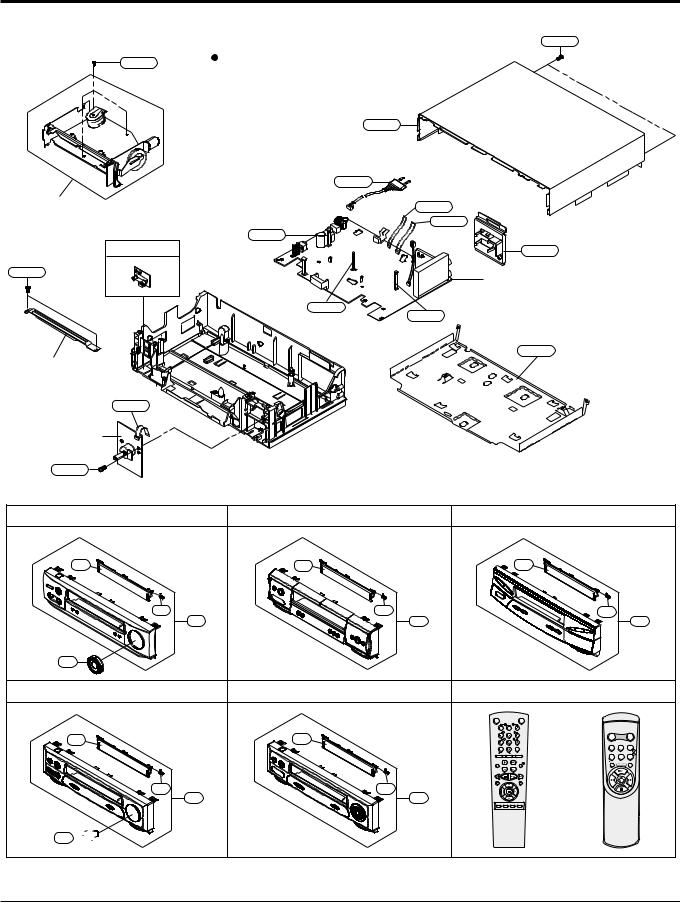
3-1 Cabinet Assembly
155
153 |
S.N.A : Service Not Available |
|
|
101 |
|
200 |
FULL DECK (S.N.A) |
CN602S |
|
|
|
CN3A1S |
|
S601A |
F-A/V PCB (S.N.A.) |
TM401B |
157 |
MAIN PCB (S.N.A.) |
|
LD601A
S602A
102
BRACKET-FRAME (S.N.A)
CN703S
SHUTTLE PCB (S.N.A.)
157
SVR-443/243 |
SVR-440/240B/240W |
SVR-2401/VCP-007LR |
21 |
21 |
21 |
22 |
22 |
22 |
1 |
1 |
1 |
55
SVR-141 |
|
SVR-140 |
|
UT01 |
|
|
|
VCR STANDBY/ON |
TV STANDBY/ON |
|
|
|
|
SLOW |
|
|
|
|
21 |
SHUTTLE |
|
STANDBY/ON |
DISPLAY |
21 |
V-LOCK |
|
|
|
|
CLR/RST F.ADV |
INDEX |
CNT.RESET SPEED |
|
||
|
|
-/-- |
|
|
|
|
|
TV SELECT VCR |
INPUT |
IIP/S IPC |
TRK |
|
|
|
REPEAT |
|
|
|
|
AUDIO |
DISP./ |
REC |
MENU |
|
|
REPEAT |
|||
|
|
VOL PROG/TRK |
|
|
|
|
|
REC |
MENU |
|
|
22 |
|
22 |
|
|
|
1 |
|
1 |
|
|
|
SPEED DUB TV/VCR TIMER
55 

3-2 |
Samsung Electronics |
|
|
|
|
|
|
|
|
|
Exploded View and Parts List |
|
|
|
|
|
|
|
|
|
|
Loc. No |
Parts No. |
|
Description ; Specification |
|
Remark |
||||
1 |
Refer to table below |
ASSY-PANEL FRONT |
|
|
|||||
21 |
Refer to table below |
DOOR-CASSETTE |
|
|
|||||
22 |
AC61-62032A |
|
SPRING-MASK;X-9,-,SUS,-,4.4,-,SV-C130 |
|
|
||||
55 |
AC64-00587A |
|
KNOB-SHUTTLE;SVR-643,ABS,-,SILVER,-,-,-, |
SVR-443/243 ONLY |
|||||
|
AC64-00319A |
|
KNOB-SHUTTLE;-,ABS,-,GRAY,HB,SV-130G,- |
SVR-141 ONLY |
|||||
101 |
Refer to table below |
CABINET TOP |
|
|
|
|
|||
102 |
AC63-00015A |
|
COVER-BOTTOM;-,SECC,-,T;0.5,SECC T0.5,-, |
|
|||||
153 |
AC60-12126A |
|
SCREW-BH;-,BH,-,4*12,FE,FZY,-,-,- |
|
|
||||
155 |
AC60-12134A |
|
SCREW-TAP BH;-,BH,-,2-4X16,-,FE |
|
|
||||
157 |
AC60-10063A |
|
SCREW-TAPTITE;BH,+,-,M3,L12,ZPC3,SWRCH18 |
|
|||||
200 |
AC39-10019A |
|
POWER CORD;KKP-419C,H03VVH2-F,VDE/KEMA-K |
|
|||||
CN3A1S |
3809-001206 |
|
CABLE-FLAT;30V,-20to+80C,140mm,6P,1.25mm |
|
|||||
CN602S |
3809-001111 |
|
CABLE-FLAT;30V,80C,130mm,7P,1.25mm,UL289 |
|
|||||
CN703S |
3809-001112 |
|
CABLE-FLAT;30V,80C,130mm,5P,1.25mm,UL289 |
SVR-443/243/141 ONLY |
|||||
LD601A |
AC61-21009A |
|
HOLDER-LED;-,POM(M90-44),-,BLK,-,X-9 |
|
|
||||
S601A |
AC61-21008A |
|
HOLDER-SENSOR;-,POM(M90-44),-,BLK,-,X-9 |
|
|||||
S602A |
AC61-21008A |
|
HOLDER-SENSOR;-,POM(M90-44),-,BLK,-,X-9 |
|
|||||
UT01 |
Refer to table below |
REMOCON-ASSY |
|
|
|||||
|
|
|
|
|
|
|
|
|
|
MODELS |
|
|
1 |
|
21 |
|
101 |
UT01 |
|
|
|
|
|
|
|
|
|
||
SVR-443 |
|
AC97-01363B |
|
AC64-00572Q |
|
AC64-00400A |
AC59-00048A |
||
|
|
|
|
|
|
|
|
||
SVR-440 |
|
AC97-01366B |
|
AC64-00536B |
|
AC64-00400B |
AC59-00048A |
||
|
|
|
|
|
|
|
|
||
SVR-243 |
|
AC97-01363C |
|
AC64-00572S |
|
AC64-00400A |
AC59-00048A |
||
|
|
|
|
|
|
|
|
||
SVR-240B |
|
AC97-01366C |
|
AC64-00536C |
|
AC64-00400B |
AC59-00048A |
||
|
|
|
|
|
|
|
|
||
SVR-240W |
|
AC97-01366D |
|
AC64-00536D |
|
AC64-00400L |
AC59-00048C |
||
|
|
|
|
|
|
|
|
||
SVR-2401 |
|
AC97-01313A |
|
AC64-00687A |
|
AC64-00400B |
AC59-00049A |
||
|
|
|
|
|
|
|
|
||
SVR-141 |
|
AC97-00873B |
|
AC64-00683U |
|
AC64-00400B |
AC59-00013C |
||
|
|
|
|
|
|
|
|
||
SVR-140 |
|
AC97-00873C |
|
AC64-00683T |
|
AC64-00400A |
AC59-00013C |
||
|
|
|
|
|
|
|
|
||
VCP-007LR |
|
AC97-01466A |
|
AC64-00687B |
|
AC64-00400B |
AC59-00013C |
||
|
|
|
|
|
|
|
|
|
|
Samsung Electronics |
3-3 |
Exploded View and Parts List
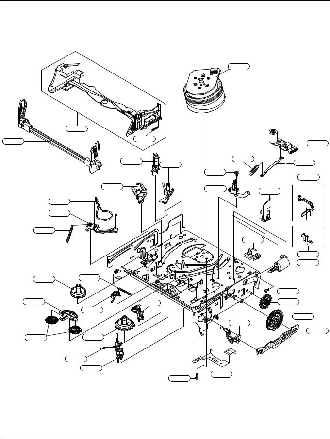
3-2 Mechanical Parts (Top Side)
G001
|
K490 |
|
|
|
|
K530 |
|
|
K502 |
|
G555 |
|
|
|
|
||
|
|
|
|
|
|
|
|
G530 |
G450 |
B473 |
B474 |
|
|
|
|||
|
|
|
|
|
|
|
|
|
G510 |
|
G680 |
|
|
|
|
|
|
|
G420 |
|
G480 |
K546 |
(OPTIONAL) |
|
|
|
|||
|
|
|
|
||
|
K250 |
|
|
|
|
|
K240 |
|
|
|
|
K248 |
|
|
|
|
(OPTIONAL) |
|
|
|
|
B575 |
|
|
|
|
|
|
G681 |
|
|
|
|
|
B410 |
K110 |
K350 |
|
|
|
|
|
|
|
|
|
B440 |
K182 |
K330 |
|
K340 |
|
B448 |
|
|
|
|
B452 |
|
|
|
|
|
G546 |
|
|
|
|
|
|
|
K188 |
K140 |
|
|
|
K470 |
|
|
|
|
G527
G520
G070
G060
3-4 |
Samsung Electronics |

|
|
|
Exploded View and Parts List |
|
|
|
|
Loc. No |
Parts No. |
Description ; Specification |
Remark |
B410 |
AC31-00012A |
MOTOR-LOADING ASSY;-,TS-10,-,-,-,-,-,-,- |
|
B440 |
AC60-10515A |
SCREW-MACHINE;-,PH,+,-,M3,L3,ZPC,-,YEL |
|
B448 |
AC66-00008A |
GEAR-WORM WHEEL;TS-10,POM,0.8,40,-,NAT,3 |
|
B452 |
AC66-00011A |
GEAR-FL CAM;TS-10,POM,0.8,59,-,BLK,48.48 |
|
B473 |
AC61-00105A |
SPRING-PINCH DRIVE;TS-10,SUS304-WPB,-,-, |
|
B474 |
AC61-30180A |
PLATE-JOINT;-,SECC20/20,T0.8,-,X-9 |
|
B575 |
AC47-00002A |
DAMPER-CAPSTAN;TS-10,POM,-,-,BLACK |
|
G001 |
AC97-01212A |
ASSY-CYLINDER;PALCTS10,4HD/DLC |
4HEAD |
|
AC97-01208A |
ASSY-CYLINDER;PAL,CTS10,2HD(LP)/DLC |
2HEAD |
|
AC97-01209A |
ASSY-CYLINDER;PAL,CTS10,2HD(LP) |
VCP |
G060 |
6006-001092 |
SCREW-ASS’Y MACH;WS,PH,+,M3.0,L6.0,ZPC(Y |
|
G070 |
AC61-00161A |
PLATE-GROUND DECK;TS-10,SPTE,T0.3,- |
|
G420 |
AC66-80142A |
SLIDER-SUPPLY ASSY;-,X-9(TS),-,-,-,X-9 |
|
G450 |
AC66-80141A |
SLIDER-TAKE UP ASSY;-,X-9(TS),-,-,-,X-9 |
|
G480 |
AC33-00009A |
HEAD-ACE ASS’Y;-,PPS,TS-10,-,- |
|
G510 |
6006-001075 |
SCREW-ASS’Y TAPT;WSP,PH,+,M2.6,L5.0,ZPC( |
|
G520 |
AC66-00033A |
LEVER-#9 GUIDE ASS’Y;TS-10,-,-,-,-,-,-,- |
|
G527 |
AC61-60553A |
SPRING-#9 GUIDE;-,ES,SUS304-WPB,OD3.1,0. |
|
G530 |
AC33-00007A |
HEAD-FE;-,-,HVFHPOO43A,-,- |
|
G546 |
AC66-00005A |
LEVER-FL DOOR;TS-10,POM,-,-,-,-,NAT,- |
|
G555 |
AC66-00032A |
LEVER-UNIT PINCH ASS’Y;TS-10,-,-,-,-,-,- |
|
G680 |
AC66-00046A |
LEVER-HEAD CLEANER ASS’Y;TS-10,POM+URETH |
(OPTIONAL) |
G681 |
AC61-50686A |
SLEEVE-HEAD CLEANER;-,POM,-,-,-,-,-,-,TS |
(OPTIONAL) |
K110 |
AC66-10267A |
REEL-DISK S;X-9,POM,-,-,-,-,-,- |
|
K140 |
AC66-10268A |
REEL-DISK T;X-9,POM,-,-,-,-,-,- |
|
K182 |
AC66-30524A |
LEVER-IDLER;-,POM,-,-,-,-,-,- |
|
K188 |
AC66-00039A |
GEAR-IDLE;TS-10,PET K3372,0.5,-,-,NTR,28 |
|
K240 |
AC66-00035A |
LEVER-TENSION ASS’Y;TS-10,SECC E20/20+SU |
|
K248 |
AC61-00107A |
SPRING-TENSION LEVER;TS-10,SUS304-WPB,-, |
|
K250 |
AC69-00104A |
BAND-BRAKE ASS’Y;TS-10,-,-,-,-,-,- |
|
K330 |
AC66-30550A |
LEVER-S.BRAKE ASSY;-,POM+SUS,-,-,-,X-9 |
|
K340 |
AC66-30549A |
LEVER-T.BRAKE ASSY;-,POM+SUS,-,-,-,X-9 |
|
K350 |
AC61-00106A |
SPRING-BRAKE;TS-10,SUS304-WPB,-,-,-,-,-, |
|
K470 |
AC66-00020A |
SLIDER-FL DRIVE;TS-10,SECC E20/20,1.0,-, |
|
K490 |
AC61-00120A |
HOLDER-FL CASS. ASS’Y;TS-10,-,-,-,-,- |
|
K502 |
AC61-60561A |
SPRING-FL.LEVER-LR;-,ES,SUS304 WPB,PI2.7 |
|
K530 |
AC66-00034A |
LEVER-FL ARM ASS’Y;TS-10,-,-,-,-,-,-,- |
|
K546 |
AC61-50658A |
GUIDE-CASS. DOOR;X-9,POM,-,NTR,-,- |
|
Samsung Electronics |
3-5 |
Exploded View and Parts List
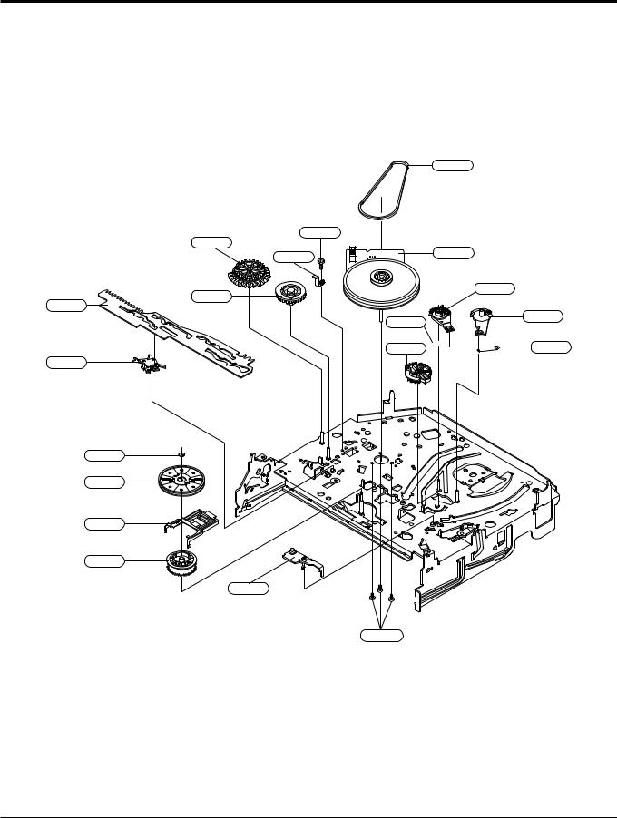
3-3 Mechanical Parts (Bottom Side)
G542
B462
B456 |
|
B560 |
B460 |
|
|
|
|
|
B458 |
|
B500 |
|
|
|
B464 |
|
B488 |
|
B501 |
|
|
|
B484 
 B489
B489
B468
K222
K200
K225
K221
B478
B570
3-6 |
Samsung Electronics |

|
|
|
Exploded View and Parts List |
|
|
|
|
Loc. No |
Parts No. |
Description ; Specification |
Remark |
B456 |
AC66-00009A |
GEAR-JOINT 1;TS-10,POM,1.5,17.5(22),-,NA |
|
B458 |
AC66-00012A |
GEAR-JOINT 2;TS-10,POM,1.0,23,-,BLK,24.6 |
|
B460 |
AC61-00090A |
BRACKET-GEAR;TS-10,0.8,-,- |
|
B462 |
AC60-10517A |
SCREW-TAP TITE;-,PH,+,-,M2.6,L5,ZPC,-,YE |
|
B464 |
AC66-00019A |
SLIDER-CAM;TS-10,SECC E20/20,1.2,-,-,-,- |
|
B468 |
AC66-00017A |
LEVER-PINCH DRIVE;TS-10,SECC E20/20,1.0 |
|
B478 |
AC66-00016A |
LEVER-TENSION DRIVE;TS-10,SECC E20/20,1 |
|
B484 |
AC66-00030A |
GEAR-LOADING DR. ASS’Y;TS-10,POM+SWPB,-, |
|
B488 |
AC66-00023A |
LEVER-S LOADING;TS-10,POM,-,-,-,-,NAT,- |
|
B489 |
AC66-00021A |
LINK-LOADING S;TS-10,SECC E20/20,0.8,-,- |
|
B500 |
AC66-00024A |
LEVER-T LOADING;TS-10,POM,-,-,-,-,NAT,- |
|
B501 |
AC66-00022A |
LINK-LOADING T;TS-10,SECC E20/20,0.8,-,- |
|
B560 |
AC31-00010A |
MOTOR-CAPSTAN;-,SANKYO,-,- |
|
B570 |
AC60-10514A |
SCREW-CAPSTAN;-,PH,+,M2.6,L6,- |
|
G542 |
AC66-60051A |
BELT-PULLEY;-,5CM-70,2 * 2,-,71.3,-,X-9 |
|
K200 |
AC61-21012A |
HOLDER-CLUTCH ASSY;-,-,-,-,-,X-9 |
|
K221 |
AC66-20581A |
GEAR-CENTER ASSY;-,POM,M=O.5,-,HIGHT T., |
|
K222 |
AC60-30306A |
WASHER-SLIT;-,-,ID2.1,OD5.0,T0.5,-,POLYS |
|
K225 |
AC66-00006A |
LEVER-UP DOWN;TS-10,POM,-,-,-,-,NAT,- |
|
Samsung Electronics |
3-7 |

Exploded View and Parts List
MEMO
3-8 |
Samsung Electronics |
4. Electrical Parts List
Loc.No |
Part No |
Description ; Specification |
- |
- |
ASSY PCB-MAIN-FULL |
S.M.P.S. PARTS |
|
|
BD1SD1 |
AC27-92001M |
INDUCTOR;70UH-M RT BFS3565R2F,-,-,-,- |
BD1SF1 |
3301-000297 |
CORE-FERRITE BEAD;AA,3.6x1.2x5.7mm,1400, |
BD1SF3 |
AC27-92001M |
INDUCTOR;70UH-M RT BFS3565R2F,-,-,-,- |
BD1SR1 |
3301-000297 |
CORE-FERRITE BEAD;AA,3.6x1.2x5.7mm,1400, |
BD1SS2 |
AC27-92001M |
INDUCTOR;70UH-M RT BFS3565R2F,-,-,-,- |
BD1SS3 |
3301-000297 |
CORE-FERRITE BEAD;AA,3.6x1.2x5.7mm,1400, |
C1SD03 |
2201-000812 |
C-CERAMIC,DISC;2.2nF,20%,400V,Y5U,BK,12. |
C1SD04 |
2201-000812 |
C-CERAMIC,DISC;2.2nF,20%,400V,Y5U,BK,12. |
C1SD11 |
2401-001682 |
C-AL;82uF,20%,400V,GP,BK,22x25,10 |
C1SD11 |
2401-003302 |
C-AL;47uF,20%,400V,GP,TP,18X31.5,7. |
C1SD12 |
2305-001029 |
C-FILM,MPEF;10nF,10%,630V,TP,12x9x12.5,5 |
C1SD13 |
2201-000376 |
C-CERAMIC,DISC;0.22nF,5%,50V,SL,TP,6.3x3 |
C1SD13 |
2301-000361 |
C-FILM,PEF;1.2nF,10%,50V,TP,-,5mm |
C1SF12 |
2401-001200 |
C-AL;33uF,20%,50V,WT,TP,6.3x11,5 |
C1SR12 |
2401-000905 |
C-AL;22uF,20%,16V,BP,-,6x11,2.5mm |
C1SR14 |
2301-000445 |
C-FILM,PEF;4.7nF,5%,50V,TP,5.5x7x3mm,5mm |
C1SS01 |
2305-001021 |
C-FILM,MPEF;100nF,20%,275V,TP,17.5x7x13. |
C1SS02 |
2305-001021 |
C-FILM,MPEF;100nF,20%,275V,TP,17.5x7x13. |
C1SS03 |
2301-000361 |
C-FILM,PEF;1.2nF,10%,50V,TP,-,5mm |
C1SS12 |
2201-000129 |
C-CERAMIC,DISC;0.1nF,10%,1kV,Y5P,TP,7x4, |
C1SS31 |
2401-000385 |
C-AL;10uF,20%,100V,GP,TP,6.3x11,5 |
C1SS32 |
2401-003137 |
C-AL;330UF,20%,50V,WT,TP,10X16MM,5 |
C1SS33 |
2401-001126 |
C-AL;330uF,20%,25V,WT,TP,10x12.5,5 |
C1SS34 |
2401-003477 |
C-AL;330UF,20%,25V,LZ,TP,10X12.5MM, |
C1SS35 |
2401-003480 |
C-AL;1000UF,20%,10V,LZ,TP,10X16MM,5 |
C1SS36 |
2401-001479 |
C-AL;470uF,20%,10V,GP,TP,-,- |
C1SS39 |
2301-000129 |
C-FILM,PEF;100nF,5%,50V,TP,10X9X4.3X5,5m |
CN1SS1 |
3711-000178 |
CONNECTOR-HEADER;1WALL,2P,1R,3.96mm,STRA |
D1SD11 |
0402-001195 |
DIODE-RECTIFIER;F1T4,400V,1.0A,TS-1,TP |
D1SD31 |
0402-001195 |
DIODE-RECTIFIER;F1T4,400V,1.0A,TS-1,TP |
D1SF05 |
0402-001196 |
DIODE-RECTIFIER;1T5,600V,1A,TS-1,TP |
D1SF12 |
0402-001195 |
DIODE-RECTIFIER;F1T4,400V,1.0A,TS-1,TP |
D1SR11 |
0401-000101 |
DIODE-SWITCHING;1N4148,100V,200mA,DO-35, |
D1SS01 |
0402-001196 |
DIODE-RECTIFIER;1T5,600V,1A,TS-1,TP |
D1SS02 |
0402-001196 |
DIODE-RECTIFIER;1T5,600V,1A,TS-1,TP |
D1SS03 |
0402-001196 |
DIODE-RECTIFIER;1T5,600V,1A,TS-1,TP |
D1SS04 |
0402-001196 |
DIODE-RECTIFIER;1T5,600V,1A,TS-1,TP |
D1SS11 |
0402-000012 |
DIODE-RECTIFIER;UF4007,1KV,1A,DO-41,TP |
D1SS30 |
0402-000127 |
DIODE-RECTIFIER;1N4002,100V,1A,DO-41,TP |
D1SS31 |
0402-001195 |
DIODE-RECTIFIER;F1T4,400V,1.0A,TS-1,TP |
D1SS32 |
0402-001194 |
DIODE-RECTIFIER;UG2D,200V,2A,DO-204AC,TP |
D1SS33 |
0402-000431 |
DIODE-RECTIFIER;FML-M02S,200V,2.5A,TO-22 |
F1SS01 |
3601-001123 |
FUSE-CARTRIDGE;250V,1.6A,TIME-LAG,CERAMI |
IC1SF1 |
1203-001802 |
IC-PWM CONTROLLER;STR-G6551,TO-220F,5P,- |
IC1SS1 |
0604-001028 |
PHOTO-COUPLER;TR,50-600%,250mW,DIP-4,ST |
IC1SS2 |
AC14-12006D |
IC;KA431Z,TO-92,TAPING |
L1SS02 |
AC29-00002A |
FILTER LINE NOISE;-,30mH,-,-,BLF-2116 |
L1SS31 |
AC27-12001N |
COIL-CHOKE;10UH-15%,RA,K-30,Q80,150KHZ,- |
L1SS32 |
AC27-12001N |
COIL-CHOKE;10UH-15%,RA,K-30,Q80,150KHZ,- |
PT1SS1 |
AC26-00002C |
TRANS SWITCHING;-,-,EE2621,-,UL/CSA/DEMK |
PT1SS1 |
AC26-00002G |
TRANS SWITCHING;EE2621,SV-643F,-,230V,FE |
Q1SR01 |
0502-001050 |
TR-POWER;2SC4517A,NPN,30W,TO-220,ST,10- |
Q1SR02 |
0501-000442 |
TR-SMALL SIGNAL;KTC3203-Y,NPN,400MW,T0-9 |
R1SD11 |
2001-000305 |
R-CARBON;110KOHM,5%,1/8W,AA,TP,1.8X3.2MM |
R1SD12 |
2001-000325 |
R-CARBON;120OHM,5%,1/8W,AA,TP,1.8X3.2MM |
R1SD12 |
2001-000003 |
R-CARBON;330ohm,5%,1/8W,AA,TP,1.8x3.2mm |
R1SD13 |
2001-000076 |
R-CARBON;47KOHM,5%,1/4W,AA,TP,2.4X6.4MM |
R1SD13 |
2001-000305 |
R-CARBON;110KOHM,5%,1/8W,AA,TP,1.8X3.2MM |
R1SD14 |
2001-000076 |
R-CARBON;47KOHM,5%,1/4W,AA,TP,2.4X6.4MM |
Remark
S.N.A.
Not used SVR-2401 Not used SVR-2401 SVR-2401 ONLY
SVR-2401 ONLY
SVR-2401 ONLY Not used SVR-2401 SVR-2401 ONLY SVR-2401 ONLY
Not used SVR-2401
Not used SVR-2401 Not used SVR-2401 SVR-2401 ONLY
Not used SVR-2401
SVR-2401 ONLY
SVR-2401 ONLY
SVR-2401 ONLY
SVR-2401 ONLY
SVR-2401 ONLY
SVR-2401 ONLY
Loc.No |
Part No |
Description ; Specification |
R1SD14 |
2001-000305 |
R-CARBON;110KOHM,5%,1/8W,AA,TP,1.8X3.2MM |
R1SD15 |
2001-000076 |
R-CARBON;47KOHM,5%,1/4W,AA,TP,2.4X6.4MM |
R1SD15 |
2001-000305 |
R-CARBON;110KOHM,5%,1/8W,AA,TP,1.8X3.2MM |
R1SD16 |
2003-000994 |
R-METAL OXIDE(S);33Kohm,5%,2W,AF,TP,3.9x |
R1SD31 |
2001-000780 |
R-CARBON;470OHM,5%,1/8W,AA,TP,1.8X3.2MM |
R1SD31 |
2001-000515 |
R-CARBON;220OHM,5%,1/8W,AA,TP,1.8X3.2MM |
R1SD32 |
2001-000429 |
R-CARBON;1KOHM,5%,1/8W,AA,TP,1.8X3.2MM |
R1SD32 |
2001-000221 |
R-CARBON;1.2KOHM,5%,1/8W,AA,TP,1.8X3.2M |
R1SF11 |
2001-000076 |
R-CARBON;47KOHM,5%,1/4W,AA,TP,2.4X6.4MM |
R1SF15 |
2001-000591 |
R-CARBON;3.3KOHM,5%,1/8W,AA,TP,1.8X3.2M |
R1SF19 |
2001-000904 |
R-CARBON;620OHM,5%,1/8W,AA,TP,1.8X3.2MM |
R1SF20 |
2003-002197 |
R-METAL OXIDE;0.47ohm,5%,2W,AF,TP,3.9x10 |
R1SF21 |
2001-000096 |
R-CARBON(S);1MOHM,5%,1/2W,AA,TP,2.4X6.4M |
R1SR11 |
2003-000119 |
R-METAL OXIDE;0.68ohm,5%,2W,AE,TP,6x16mm |
R1SR12 |
2003-000264 |
R-METAL OXIDE;300ohm,5%,1W,AD,TP,4.3x12m |
R1SR14 |
2001-000003 |
R-CARBON;330ohm,5%,1/8W,AA,TP,1.8x3.2mm |
R1SS10 |
2006-000262 |
R-CEMENT;2.7ohm,10%,2W,CB,TP,7.5x11x20. |
R1SS11 |
2003-000994 |
R-METAL OXIDE(S);33Kohm,5%,2W,AF,TP,3.9x |
R1SS13 |
2003-000148 |
R-METAL OXIDE;100OHM,5%,2W,AE,TP,6X16MM |
R1SS32 |
2001-000429 |
R-CARBON;1KOHM,5%,1/8W,AA,TP,1.8X3.2MM |
R1SS33 |
2004-000869 |
R-METAL;3Kohm,1%,1/8W,AA,TP,1.8x3.2mm |
R1SS34 |
2004-000459 |
R-METAL;2.2Kohm,1%,1/8W,AA,TP,1.8x3.2m |
VA1SS1 |
1405-001026 |
VARISTOR;470V,600A,9x7mm,TP |
ZD1SS1 |
0403-000571 |
DIODE-ZENER;UZP43B,43V,40-46V,1W,DO-41,T |
POWER DRIVE PARTS |
|
|
C1P102 |
2401-001545 |
C-AL;47uF,20%,25V,GP,TP,6.3x7mm,2.5 |
C1P103 |
2401-000598 |
C-AL;1uF,20%,50V,GP,TP,4x7,5 |
C1P104 |
2401-002299 |
C-AL;4.7uF,20%,50V,GP,TP,5x7,5 |
C1P105 |
2401-003107 |
C-AL;47uF,20%,16V,GP,TP,5x7,5 |
C1P106 |
2401-003107 |
C-AL;47uF,20%,16V,GP,TP,5x7,5 |
C1P108 |
2401-001573 |
C-AL;47uF,20%,50V,GP,TP,6.3x11,2.5 |
D1P101 |
0401-000101 |
DIODE-SWITCHING;1N4148,100V,200mA,DO-35, |
Q1P101 |
0501-000616 |
TR-SMALL SIGNAL;KSC2328A-Y,NPN,1W,TO-92L |
Q1P102 |
0501-000616 |
TR-SMALL SIGNAL;KSC2328A-Y,NPN,1W,TO-92L |
Q1P104 |
0501-002268 |
TR-SMALL SIGNAL;STB1277,PNP,625mW,TO-92, |
Q1P105 |
0504-000116 |
TR-DIGITAL;KSR1001,NPN,300MW,4.7K/4.7K,T |
R1P101 |
2001-000855 |
R-CARBON;560OHM,5%,1/4W,AA,TP,2.4X6.4MM |
R1P101 |
2001-000034 |
R-CARBON;220OHM,5%,1/4W,AA,TP,2.4X6.4MM |
R1P106 |
2001-000449 |
R-CARBON;2.2KOHM,5%,1/8W,AA,TP,1.8X3.2M |
R1P107 |
2001-000273 |
R-CARBON;100KOHM,5%,1/8W,AA,TP,1.8X3.2M |
R1P108 |
2001-000611 |
R-CARBON;3.9KOHM,5%,1/4W,AA,TP,2.4X6.4M |
R1P115 |
2001-000554 |
R-CARBON;270OHM,5%,1/8W,AA,TP,1.8X3.2MM |
R1P116 |
2001-000563 |
R-CARBON;27KOHM,5%,1/8W,AA,TP,1.8X3.2MM |
ZD1P02 |
0403-000717 |
DIODE-ZENER;MTZJ5.1B,5.1V,4.94-5.2V,500m |
ZD1P04 |
0403-000720 |
DIODE-ZENER;MTZJ9.1B,9.1V,8.57-9.01V,500 |
SYSTEM CONTROL/SERVO PARTS |
|
|
C601 |
2401-003107 |
C-AL;47uF,20%,16V,GP,TP,5x7,5 |
C602C |
2203-000609 |
C-CERAMIC,CHIP;22nF,10%,50V,X7R,TP,2012 |
C603C |
2203-000891 |
C-CERAMIC,CHIP;4.7nF,10%,50V,X7R,TP,2012 |
C604C |
2203-000891 |
C-CERAMIC,CHIP;4.7nF,10%,50V,X7R,TP,2012 |
C605C |
2203-000260 |
C-CERAMIC,CHIP;10nF,10%,50V,X7R,TP,2012 |
C606C |
2203-000260 |
C-CERAMIC,CHIP;10nF,10%,50V,X7R,TP,2012 |
C607 |
2401-000118 |
C-AL;1000uF,20%,10V,GP,TP,10x12.5,5 |
C608C |
2203-000575 |
C-CERAMIC,CHIP;220NF,10%,25V,X7R,TP,2012 |
C609C |
2203-000609 |
C-CERAMIC,CHIP;22nF,10%,50V,X7R,TP,2012 |
C611C |
2203-001579 |
C-CERAMIC,CHIP;15nF,10%,50V,NP0,TP,2012 |
C612 |
2202-002037 |
C-CERAMIC,MLC-AXIAL;100nF,80-20%,50V,Y5V |
C613C |
2203-000609 |
C-CERAMIC,CHIP;22nF,10%,50V,X7R,TP,2012 |
C615C |
2203-000444 |
C-CERAMIC,CHIP;1nF,10%,50V,X7R,TP,2012,- |
C616 |
2202-000807 |
C-CERAMIC,MLC-AXIAL;22nF,+80-20%,25V,Y5V |
Remark
SVR-2401 ONLY
SVR-2401 ONLY
SVR-2401 ONLY
SVR-2401 ONLY Not used SVR-2401 Not used SVR-2401 Not used SVR-2401 Not used SVR-2401 Not used SVR-2401
SVR-2401 ONLY SVR-2401 ONLY SVR-2401 ONLY
Not used SVR-2401
SVR-2401 ONLY
VCP ONLY
VCP ONLY
Samsung Electronics |
4-1 |

Electrical Parts List
Loc.No |
Part No |
Description ; Specification |
Remark |
|
Loc.No |
Part No |
Description ; Specification |
Remark |
C617 |
2401-000591 |
C-AL;1uF,20%,50V,BP,TP,3x5,2.5mm |
|
|
R654 |
2001-000812 |
R-CARBON;5.6KOHM,5%,1/8W,AA,TP,1.8X3.2M |
|
C618 |
2401-000360 |
C-AL;100uF,20%,50V,GP,TP,8x11.5,5 |
|
|
R655C |
2007-000941 |
R-CHIP;47KOHM,5%,1/10W,DA,TP,2012 |
|
C619C |
2203-000260 |
C-CERAMIC,CHIP;10nF,10%,50V,X7R,TP,2012 |
|
|
R656C |
2007-000241 |
R-CHIP;1.5KOHM,5%,1/10W,DA,TP,2012 |
|
C620C |
2203-000192 |
C-CERAMIC,CHIP;100nF,+80-20%,50V,Y5V,TP, |
|
|
R657 |
2001-000010 |
R-CARBON;68KOHM,5%,1/8W,AA,TP,1.8X3.2MM |
Not used VCP |
C621 |
2401-000118 |
C-AL;1000uF,20%,10V,GP,TP,10x12.5,5 |
|
|
R660 |
2001-000786 |
R-CARBON;47KOHM,5%,1/8W,AA,TP,1.8X3.2MM |
|
C622C |
2203-001680 |
C-CERAMIC,CHIP;68nF,20%,50V,Z5U,TP,2012 |
|
|
R661 |
2001-000660 |
R-CARBON;33KOHM,5%,1/8W,AA,TP,1.8X3.2MM |
|
C623C |
2203-000609 |
C-CERAMIC,CHIP;22nF,10%,50V,X7R,TP,2012 |
|
|
R666C |
2007-000931 |
R-CHIP;470OHM,5%,1/10W,DA,TP,2012 |
|
C624 |
2202-000205 |
C-CERAMIC,MLC-AXIAL;22pF,5%,50V,SL,TP,1. |
Not used VCP |
R667C |
2007-000931 |
R-CHIP;470OHM,5%,1/10W,DA,TP,2012 |
|
|
C625 |
2202-000205 |
C-CERAMIC,MLC-AXIAL;22pF,5%,50V,SL,TP,1. |
Not used VCP |
R668C |
2007-000300 |
R-CHIP;10KOHM,5%,1/10W,DA,TP,2012 |
|
|
C626C |
2203-000634 |
C-CERAMIC,CHIP;0.022nF,5%,50V,NP0,TP,201 |
|
|
R669C |
2007-000300 |
R-CHIP;10KOHM,5%,1/10W,DA,TP,2012 |
|
C627C |
2203-000634 |
C-CERAMIC,CHIP;0.022nF,5%,50V,NP0,TP,201 |
|
|
R670 |
2001-000734 |
R-CARBON;4.7KOHM,5%,1/8W,AA,TP,1.8X3.2M |
|
C629C |
2203-000444 |
C-CERAMIC,CHIP;1nF,10%,50V,X7R,TP,2012,- |
|
|
R671 |
2001-000734 |
R-CARBON;4.7KOHM,5%,1/8W,AA,TP,1.8X3.2M |
|
C633C |
2203-000260 |
C-CERAMIC,CHIP;10nF,10%,50V,X7R,TP,2012 |
|
|
R672 |
2001-000734 |
R-CARBON;4.7KOHM,5%,1/8W,AA,TP,1.8X3.2M |
|
C634C |
2203-000260 |
C-CERAMIC,CHIP;10nF,10%,50V,X7R,TP,2012 |
|
|
R673 |
2001-000273 |
R-CARBON;100KOHM,5%,1/8W,AA,TP,1.8X3.2M |
|
C635C |
2203-000495 |
C-CERAMIC,CHIP;2.2nF,10%,50V,X7R,TP,2012 |
|
|
R674 |
2001-000290 |
R-CARBON;10KOHM,5%,1/8W,AA,TP,1.8X3.2MM |
|
C636C |
2203-000495 |
C-CERAMIC,CHIP;2.2nF,10%,50V,X7R,TP,2012 |
|
|
R675 |
2001-000032 |
R-CARBON;180OHM,5%,1/4W,AA,TP,2.4X6.4MM |
|
C637C |
2203-000938 |
C-CERAMIC,CHIP;0.47nF,5%,50V,NP0,TP,2012 |
|
|
R676 |
2001-000633 |
R-CARBON;30KOHM,5%,1/8W,AA,TP,1.8X3.2MM |
|
C638 |
2401-002299 |
C-AL;4.7uF,20%,50V,GP,TP,5x7,5 |
|
|
R677 |
2001-000522 |
R-CARBON;22KOHM,5%,1/8W,AA,TP,1.8X3.2MM |
|
C639C |
2203-000239 |
C-CERAMIC,CHIP;0.1nF,5%,50V,NP0,TP,2012 |
|
|
R678 |
2001-000522 |
R-CARBON;22KOHM,5%,1/8W,AA,TP,1.8X3.2MM |
|
C640 |
2401-001507 |
C-AL;47uF,20%,16V,GP,TP,6.3x5,5 |
|
|
R679 |
2001-000515 |
R-CARBON;220OHM,5%,1/8W,AA,TP,1.8X3.2MM |
|
C641 |
2401-002165 |
C-AL;100uF,20%,16V,GP,TP,6.3x7,5 |
|
|
R682C |
2007-000586 |
R-CHIP;22KOHM,5%,1/10W,DA,TP,2012 |
|
C644C |
2203-000595 |
C-CERAMIC,CHIP;0.22nF,5%,50V,NP0,TP,2012 |
|
|
R685C |
2007-000774 |
R-CHIP;33KOHM,5%,1/10W,DA,TP,2012 |
|
C646C |
2203-000192 |
C-CERAMIC,CHIP;100nF,+80-20%,50V,Y5V,TP, |
|
|
R686 |
2001-000429 |
R-CARBON;1KOHM,5%,1/8W,AA,TP,1.8X3.2MM |
|
C651C |
2203-000609 |
C-CERAMIC,CHIP;22nF,10%,50V,X7R,TP,2012 |
|
|
R687 |
2001-000429 |
R-CARBON;1KOHM,5%,1/8W,AA,TP,1.8X3.2MM |
|
C652C |
2203-000609 |
C-CERAMIC,CHIP;22nF,10%,50V,X7R,TP,2012 |
|
|
R688 |
2001-000429 |
R-CARBON;1KOHM,5%,1/8W,AA,TP,1.8X3.2MM |
|
C653C |
2203-000609 |
C-CERAMIC,CHIP;22nF,10%,50V,X7R,TP,2012 |
|
|
R690C |
2007-001039 |
R-CHIP;56KOHM,5%,1/10W,DA,TP,2012 |
|
C679 |
2202-000807 |
C-CERAMIC,MLC-AXIAL;22nF,+80-20%,25V,Y5V |
SHUTTLE MODELS ONLY |
R691C |
2007-000572 |
R-CHIP;220OHM,5%,1/10W,DA,TP,2012 |
|
|
C690C |
2203-000989 |
C-CERAMIC,CHIP;47nF,10%,50V,X7R,TP,2012 |
|
|
R692 |
2001-000568 |
R-CARBON;27OHM,5%,1/8W,AA,TP,1.8X3.2MM |
Not used VCP |
C691C |
2203-000260 |
C-CERAMIC,CHIP;10nF,10%,50V,X7R,TP,2012 |
|
|
R693C |
2007-000941 |
R-CHIP;47KOHM,5%,1/10W,DA,TP,2012 |
|
C692 |
2401-001479 |
C-AL;470uF,20%,10V,GP,TP,-,- |
|
|
R694 |
2001-000786 |
R-CARBON;47KOHM,5%,1/8W,AA,TP,1.8X3.2MM |
|
C695C |
2203-000361 |
C-CERAMIC,CHIP;0.15nF,5%,50V,NP0,TP,2012 |
|
|
R698C |
2007-000300 |
R-CHIP;10KOHM,5%,1/10W,DA,TP,2012 |
|
CN601 |
AC39-20817S |
LEAD CONNECTOR-ASSY;DP,SMH200-02,YBH200- |
|
|
R699C |
2007-000300 |
R-CHIP;10KOHM,5%,1/10W,DA,TP,2012 |
|
CN602 |
3708-001302 |
CONNECTOR-FPC/FC/PIC;7P,1.25mm,STRAIGHT, |
|
|
RS601 |
AC34-20100B |
SWITCH-REC;-,-,X-9,- |
|
CN604 |
3711-003749 |
CONNECTOR-HEADER;BOX,8P,2R,2mm,STRAIGHT, |
|
|
S601 |
0603-001011 |
PHOTO-TR;NPN,35V,6V,50mA,75mW,BK |
|
D602 |
0402-000127 |
DIODE-RECTIFIER;1N4002,100V,1A,DO-41,TP |
|
|
S602 |
0603-001011 |
PHOTO-TR;NPN,35V,6V,50mA,75mW,BK |
|
D603 |
0401-000101 |
DIODE-SWITCHING;1N4148,100V,200mA,DO-35, |
|
|
SW601 |
AC34-20100A |
SWITCH-MODE;-,-,X-9,- |
|
D604 |
0401-000101 |
DIODE-SWITCHING;1N4148,100V,200mA,DO-35, |
|
|
W038 |
2701-000002 |
INDUCTOR-AXIAL;100uH,10%,4.2x9.8mm |
|
D612 |
0402-000127 |
DIODE-RECTIFIER;1N4002,100V,1A,DO-41,TP |
|
|
W067 |
2701-000002 |
INDUCTOR-AXIAL;100uH,10%,4.2x9.8mm |
|
IC601 |
AC09-00215A |
IC MICOM;784927GF-203-3BA,SVR-643-GF,10 |
|
|
W121 |
2001-000734 |
R-CARBON;4.7KOHM,5%,1/8W,AA,TP,1.8X3.2M |
|
IC601 |
AC09-00217A |
IC MICOM;784927GF-204-3BA,SV-140G-GF,10 |
VCP ONLY |
W122 |
2001-000734 |
R-CARBON;4.7KOHM,5%,1/8W,AA,TP,1.8X3.2M |
|
|
IC604 |
AC14-12006C |
IC;KA7533,DIP,- |
|
|
W136 |
2701-000002 |
INDUCTOR-AXIAL;100uH,10%,4.2x9.8mm |
|
IC605 |
1103-001148 |
IC-EEPROM;24C021,2KBIT,DIP,8P,300MIL,10M |
|
|
W230 |
0402-000127 |
DIODE-RECTIFIER;1N4002,100V,1A,DO-41,TP |
|
IC608 |
1203-000515 |
IC-VOL. DETECTOR;7042,TO-92,3P,177MIL,PL |
Not used VCP |
W505 |
2001-000281 |
R-CARBON;100OHM,5%,1/8W,AA,TP,1.8X3.2MM |
|
|
IC610 |
1003-001318 |
IC-MOTOR DRIVER;LB11880,DIP,30P,417MIL,- |
|
|
W513 |
0402-000127 |
DIODE-RECTIFIER;1N4002,100V,1A,DO-41,TP |
|
L601 |
2701-000002 |
INDUCTOR-AXIAL;100uH,10%,4.2x9.8mm |
|
|
XT601 |
2801-003318 |
CRYSTAL-UNIT;32.768KHz,20ppm,28-AAP,12.5 |
Not used VCP |
L602 |
2701-000002 |
INDUCTOR-AXIAL;100uH,10%,4.2x9.8mm |
|
|
XT602 |
2801-003139 |
CRYSTAL-UNIT;8MHz,50ppm,28-AAA,22pF,80oh |
|
L603 |
2701-000002 |
INDUCTOR-AXIAL;100uH,10%,4.2x9.8mm |
|
|
|
|
|
|
LD601 |
0601-000517 |
LED-IR;RECTANGULA,4x6.0mm,75mW,6V,950 |
|
|
AUDIO/VIDEO PARTS |
|
|
|
PT601 |
0604-001122 |
PHOTO-INTERRUPTER;TR,0.065%,150mW,DIP-4, |
|
|
C301 |
2401-001919 |
C-AL;2.2uF,20%,50V,-,TP,4x7mm,5 |
|
PT602 |
0604-001122 |
PHOTO-INTERRUPTER;TR,0.065%,150mW,DIP-4, |
|
|
C302 |
2301-000283 |
C-FILM,PEF;47nF,5%,100V,TP,7.3X7X3.2X5,5 |
|
Q602 |
0501-000398 |
TR-SMALL SIGNAL;KSC945,NPN,250mW,TO-92,T |
|
|
C303 |
2401-000598 |
C-AL;1uF,20%,50V,GP,TP,4x7,5 |
|
R601C |
2007-001024 |
R-CHIP;560KOHM,5%,1/10W,DA,TP,2012 |
|
|
C304C |
2203-000683 |
C-CERAMIC,CHIP;0.027nF,5%,50V,NP0,TP,201 |
|
R602C |
2007-000282 |
R-CHIP;100KOHM,5%,1/10W,DA,TP,2012 |
|
|
C305 |
2202-000164 |
C-CERAMIC,MLC-AXIAL;0.18nF,10%,50V,Y5P,T |
|
R603C |
2007-000710 |
R-CHIP;3.9KOHM,5%,1/10W,DA,TP,2012 |
|
|
C306 |
2202-000231 |
C-CERAMIC,MLC-AXIAL;330pF,10%,50V,Y5P,TP |
|
R607 |
2001-000429 |
R-CARBON;1KOHM,5%,1/8W,AA,TP,1.8X3.2MM |
|
|
C307C |
2203-000392 |
C-CERAMIC,CHIP;0.015nF,5%,50V,SL,TP,2012 |
|
R608 |
2001-000864 |
R-CARBON;56KOHM,5%,1/8W,AA,TP,1.8X3.2MM |
|
|
C308C |
2203-000260 |
C-CERAMIC,CHIP;10nF,10%,50V,X7R,TP,2012 |
|
R609C |
2007-001039 |
R-CHIP;56KOHM,5%,1/10W,DA,TP,2012 |
|
|
C309 |
2401-000598 |
C-AL;1uF,20%,50V,GP,TP,4x7,5 |
|
R610 |
2001-000429 |
R-CARBON;1KOHM,5%,1/8W,AA,TP,1.8X3.2MM |
|
|
C310 |
2401-000414 |
C-AL;10uF,20%,16V,GP,TP,4x7,5 |
|
R611 |
2001-000429 |
R-CARBON;1KOHM,5%,1/8W,AA,TP,1.8X3.2MM |
|
|
C311 |
2401-000918 |
C-AL;22uF,20%,16V,GP,-,6.3x7,5 |
|
R613 |
2001-000429 |
R-CARBON;1KOHM,5%,1/8W,AA,TP,1.8X3.2MM |
Not used VCP |
C313C |
2203-000444 |
C-CERAMIC,CHIP;1nF,10%,50V,X7R,TP,2012,- |
|
|
R614 |
2001-000429 |
R-CARBON;1KOHM,5%,1/8W,AA,TP,1.8X3.2MM |
|
|
C314 |
2401-001775 |
C-AL;470nF,20%,50V,GP,TP,4x7,5 |
|
R641 |
2001-000780 |
R-CARBON;470OHM,5%,1/8W,AA,TP,1.8X3.2MM |
|
|
C315 |
2401-000414 |
C-AL;10uF,20%,16V,GP,TP,4x7,5 |
|
R642 |
2001-000780 |
R-CARBON;470OHM,5%,1/8W,AA,TP,1.8X3.2MM |
|
|
C316C |
2203-001064 |
C-CERAMIC,CHIP;56NF,10%,50V,NPO,TP,2012 |
|
R644 |
2001-000429 |
R-CARBON;1KOHM,5%,1/8W,AA,TP,1.8X3.2MM |
|
|
C318C |
2203-000192 |
C-CERAMIC,CHIP;100nF,+80-20%,50V,Y5V,TP, |
|
R650 |
2003-000111 |
R-METAL OXIDE;0.47ohm,5%,1W,AD,TP,4.3x12 |
|
|
C320 |
2401-000598 |
C-AL;1uF,20%,50V,GP,TP,4x7,5 |
|
R651C |
2007-000001 |
R-CHIP;68KOHM,5%,1/10W,DA,TP,2012 |
|
|
C321 |
2401-000414 |
C-AL;10uF,20%,16V,GP,TP,4x7,5 |
|
4-2 |
Samsung Electronics |
 Loading...