


2 Product Specifications
2 Product Specifications
2-1 Fashion Feature
-. Minimalism Design Something New
-. Boltless Model (Clean Cut & Soft Surface)
-. New Ball Hinge
-. Color Variation. White, Black
2-2 Specifications
Item |
Description |
|
|
LCD Panel |
TFT-LCD panel, RGB vertical stripe, normally black transmissive, |
|
19-Inch viewable, 0.294 (H) x 0.294 (V) mm pixel pitch |
Scanning Frequency |
Horizontal : 30 kHz ~ 81 kHz (Automatic) |
|
Vertical : 56 Hz ~ 75 Hz (UXGA : 60 Hz) |
Display Colors |
16.2 Million colors |
|
|
Maximum Resolution |
Horizontal : 1440 Pixels |
|
Vertical : 900 Pixels |
|
|
Input Signal |
Analog / Digital / Digital with HDCP |
|
|
Input Sync Signal |
Seperate H/V sync, Composite H/V, Sync-on-Green, Automatic synchroniza |
|
tion whitout external swith of sync type |
|
Level : TTL level |
|
|
Maximum Pixel Clock rate |
135 MHz |
|
|
Active Display |
376.3(H) x 301.05(W) mm |
Horizontal/Vertical |
|
|
|
AC power voltage & Frequency |
AC 90 ~ 264 Volts, 60/50 Hz |
|
|
Power Consumption |
38W (Max) |
|
|
Dimensions |
|
Set (W x D x H) |
17.7 x 14.7 x 7.8 inch (449 x 374 x 199 mm) (With stand) |
|
17.7 x 12.8 x 2.6 inch (449 x 325 x 67 mm) |
|
|
Weight (Set/Package) |
4.1kg / 5.4kg |
|
|
Environmental Considerations |
Operating Temperature : 0˚F ~ 122˚F (0 ~ 50 ) |
|
Operating Humidity : 20% ~ 90% |
|
Storage temperature : -4˚F ~ 149˚F (-20 ~ 65 ) |
|
Storage Humidity : 5% ~ 90% |
|
|
- Designs and specifications are subject to change without prior notice.
2-1

2 Product Specifications
2-4 Spec Comparison
|
Model |
|
LS19PEJ |
|
LS19PFW |
|
|
|
|
|
|
|
|
|
|
|
Design |
|
|
|
|
|
|
|
|
|
|
|
|
|
|
|
|
|
|
|
|
|
|
|
|
|
|
|
|
|
|
|
|
|
|
|
|
|
|
|
Frequency |
|
|
|
|
|
|
|
Horizontal |
|
30 ~ 81 kHz |
|
30 ~ 81 kHz |
|
|
|
Vertical |
|
60 ~ 75 Hz |
|
60 ~ 75 Hz |
|
|
|
Display Color |
|
16,2M colors |
|
16,7M colors |
|
|
|
|
|
|
|
|
|
|
|
PC Resolution |
|
1440 x 900 @ 60 Hz |
|
1440 x 900 @ 60 Hz |
|
|
|
Maximum mode |
|
1440 x 900 @75 Hz |
|
1440 x 900 @75 Hz |
|
|
|
|
|
|
|
|
|
|
|
Input Signal |
|
Analog / Digital / Digital with HDCP |
|
Analog / Digital |
|
|
|
Sync Signal |
|
Seperate, Composite, |
|
Seperate, Composite, |
|
|
|
|
|
Sync-on-Green |
|
Sync-on-Green |
|
|
|
|
|
|
|
|
|
|
|
Power |
|
|
|
|
|
|
|
Consumption |
|
42W |
|
42W |
|
|
|
Normal |
|
|
|
|
|
|
|
Power Saving |
|
< 1W |
|
< 1W |
|
|
|
|
|
|
|
|
|
|
|
Response Time |
|
2ms(G to G) |
|
2ms(G to G) |
|
|
|
|
|
|
|
|
|
|
|
Anion Option |
|
None |
|
None |
|
|
|
|
|
|
|
|
|
|
|
Magic Color |
|
Support |
|
Support |
|
|
|
|
|
|
|
|
|
|
2-2

2 Product Specifications
2-5 Option Specification |
|
|
|
Item |
Item Name |
CODE.NO |
Remark |
|
Quick Setup Guide |
BH68-00376L |
|
|
Warranty Card |
|
|
|
(Not available in all |
BH68-00633A |
|
|
locations) |
|
|
|
User's Guide, |
|
|
|
Monitor Driver, |
BN59-00585N |
|
|
Natural Color software, |
|
|
|
MagicTune™ software |
|
|
|
D-Sub(15 Pin) |
BN39-00244B |
|
|
Cable |
|
|
|
|
|
|
|
Power Cord |
3903-000042 |
|
|
Cleaning Cloth |
BN63-02368A |
(Black / High |
|
|
|
Glossy Model only) |
|
DVI Cable |
BN39-00246F |
Sold separately |
|
|
|
2-3 |

2 Product Specifications
Memo
2-4

3 Alignments and Adjustments
3 Alignments and Adjustments
This section of the service manual explains how to use the DDC MANAGER JIG. This function is needed for AD board change and program memory (IC110) change.
3-1 Required Equipment
The following equipment is necessary for adjusting the monitor:
-Computer with Windows 95, Windows 98, Windows 2000, Windows XP or Windows NT
-MTI-2055, 2058, 2059 DDC Manager Jig
3-2 Automatic Color Adjustment
To input video, use 16 gray or any pattern using black and white.
1.Select english for OSD language.
2.Press the " 

 (Enter/Source)" key for 5 seconds.
3-3 DDC EDID Data Input
1.Input DDC EDID data when replacing AD PCB.
2.Receive/Download the proper DDC file for the model from HQ quality control department. Install the below jig (Figure 1) and enter the data.
Parallel Connector
 (25P Cable)
Parallel Connector
(25P Cable)
Connect Monitor
Signal Cable
Figure 1.
3-4 OSD Adjustment When Replacing Panel
1.Adjust brightness and contrast to 0. Then, press the  (Enter/Source) key for 5 seconds. Service function OSD will appear on screen.
2.Press the + key to place the cursor on the panel. Press the menu key for 5 seconds.
3-5 OSD Adjustment When Replacing Lamp Only
1.Adjust brightness and contrast to 0. Then, press the exit key for 5 seconds. Service function OSD will appear on the screen.
2.Press the + key. Select upper lamp and press the menu key for 5 seconds. Then, select lower lamp and press the menu key for 5 seconds.
-Note : Please be sure to read the following instructions for details on service function.
3-1

3 Alignments and Adjustments
3-6 Service Function Spec.
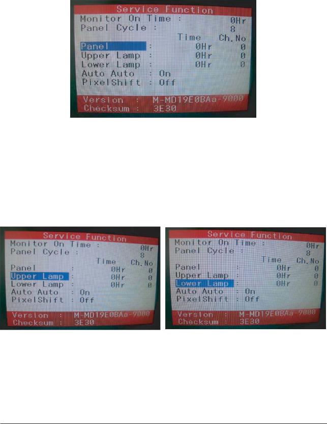
3-6-1 How to Display Service Function OSD
1.The value for brightness and contrast should be changed to zero.
2.Within 5 seconds, press the 

 (Enter/Source) key.
3.Service function OSD will be displayed.
-If you want to disable the service function OSD, you will have to power off.
Panel Information
Software Version
Checksum
Figure 2. The example of service function OSD
The service function OSD is based on a grid of 29 columns x 12 rows.
The service function OSD consists of panel information, software version and MICOM checksum.
3-6-2 How to Control Service Function OSD
1.With the panel selected on OSD, whenever you press the right key, the base color will change to blue from "Panel" to "Upper Lamp", "Lower Lamp".
Figure 2.
3-2
3 Alignments and Adjustments
3-6-3 How to Control Service Function OSD
-After changing the panel or lamp, you must reset service function OSD. -The case of panel change
After changing the panel, press the menu key within 5 seconds,.
Then, panel Ch. No increases one step and the panel time information is reset to zero. Simultaneously, other information is reset to zero (Upper/Lower lamp, Panel cycle).
Figure 4.
3-6-4 How to Control Service Function OSD
-In the case of Upper Lamp or Lower Lamp change
After changing the Upper Lamp or Lower Lamp,
1.Select the Upper Lamp or Lower Lamp
2.Press the Menu key within an 5 seconds.
Then, Ch. No and time will be reset to zero (selected item only).
Figure 5, 6.
3-3

3 Alignments and Adjustments
3-7 How to execute DDC
1.Click the Open icon
2.Select Two EDID.
3.Select a DDC file.
4.Select week 5.Click Next (OK).
6. Enter the serial number and press the Enter key.
*After entering the analog data, repeat the procedure above 2 to 5 times to enter digital data.
3-4

3 Alignments and Adjustments
3-8 How to execute MCU Code
3-8-1 Program Setting - Config Setting
1. Set the options.
-. Manufacture : MSTAR
-. Device Type :TSUM16_ROM128K_ext_flash -. Communication Port : DSUB15 (Analog)
-. External Memory : PMC25LV010E
2. Click 'LoadFile' button, and select the MCU code.
3-5

3 Alignments and Adjustments
3. Click 'Auto Program' button.
4. If Program and Verify is OK, turn off the hard power and than turn on again.
3-6
3 Alignments and Adjustments
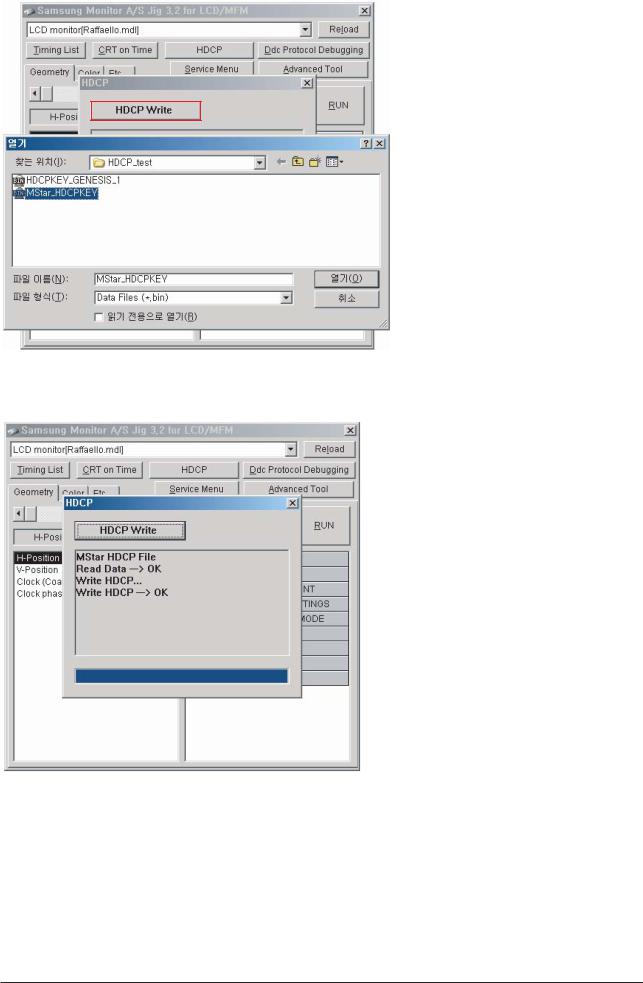
3-9 How to Execute HDCP Code
1. Execute 'service.exe'.
2. Click 'HDCP' button.2. Click 'HDCP' button.
3-7
3 Alignments and Adjustments
3. Click ' HDCP Write' button and select 'MStar_HDCPKEY'.
4. HDCP KEY writing is Complete.
3-8

4 Troubleshooting
4 Troubleshooting
Notes: 1. Before troubleshooting, setup the PC's display as below.
•Resolution: 1440 x 900
•H-frequency: 45 kHz
•V-frequency: 60 Hz
2.If no picture appears, make sure the power cord is correctly connected.
3.Check the following circuits.
•No raster appears: Function PBA, Main PBA, I/P PBA
•5V develop but no screen: Main PBA
•5V does not develop: I/P PBA
4.If you push and hold the " (Enter/Source)" button for more than 5 seconds, the monitor automatically returns to the factory preset.
4-1 No Power
|
|
|
|
|
|
Check Function Ass'y. |
|
|
|
Yes |
|
||
|
|
|
|
|
||
When Pin 4 of CN600 is 0V |
|
|
No |
|
||
does proper DC 5V, 14V |
|
|
Change IP Board. |
|||
appear at Pin 6, 7 of |
|
|
|
|||
|
|
|
||||
|
|
|
|
|||
CN600 separately? |
|
|
|
|
||
|
|
|
|
|||
|
|
Yes |
|
|
|
|
|
|
|
|
|
|
|
|
|
|
|
|
|
|
When Pin 1 of IC601 is DC 5V |
|
|
No |
|
||
|
|
|
||||
does proper DC 3.3V appear at |
|
|
Check IC601 and related circuit. |
|||
|
|
|
||||
|
|
|
||||
Pin 3 of IC603? |
|
|
|
|
||
|
|
|
|
|||
|
|
Yes |
|
|
|
|
|
|
|
|
|
|
|
|
|
|
|
|
||
When Pin3 of IC602 is DC 5V |
|
|
No |
|
||
|
|
Check IC602 and related circuit. |
||||
does proper DC1.8V appear at |
|
|
|
|||
|
|
|
||||
Pin2 of IC602? |
|
|
|
|
||
|
|
|
|
|||
4-1

4 Troubleshooting
4-2 No Video (ANALOG)
Check signal cable connection and power.
|
X1 oscillate properly? |
No |
|
|||||
1 |
|
|
||||||
|
|
|||||||
|
|
|
|
|
Yes |
|
|
|
|
|
|
|
|
|
|
||
|
|
|
|
|
|
|
||
|
|
|
|
|
|
|
No |
|
|
Is there R, G, B input at |
|
||||||
|
|
|||||||
|
R111, R114 and R118? |
|
|
|||||
|
|
|
|
|
Yes |
|
|
|
|
|
|
|
|
|
|
||
|
|
|
|
|
|
|
||
Is there Hsync, Vsync waveform |
No |
|
||||||
|
||||||||
|
2 |
|
|
3 |
|
|
|
|
|
|
|||||||
|
at Pin 32, 33 of IC 200? |
|
|
|||||
|
|
|
||||||
|
|
|
|
|
Yes |
|
|
|
|
|
|
|
|
|
|
||
|
|
|
|
|
|
|
||
Does the output signal appear |
No |
|
||||||
|
||||||||
|
at Pin 8~30 of CN400? |
|
|
|||||
|
|
|
||||||
|
|
|
|
|
Yes |
|
|
|
|
|
|
|
|
|
|
||
|
|
|
|
|
|
|
|
|
There are DC 5V at Pin 1, |
No |
|
||||||
|
2 and 3 of CN400? |
|
|
|||||
|
|
|
|
|
|
|
|
|
Yes
Replace LCD Panel.
Replace or check related circuit.
Check input part.
Check IC200 and related circuit.
Check CN400 and related circuit.
Check PANEL_EN SIGNAL at R222 is High(On:High) and BL_EN signal at R603(ON:Low) is Low
4-2

4 Troubleshooting
WAVEFORMS
1 |
2 |
3
C |
B |
C |
B |
|
|
|
|
|
|
|
|
|
|
|
|
|
|
|
|
|
|
|
|
|
|
|
|
|
|
E |
|
E |
|
|
|
|
|
|
|
|
|
|
|
|
|
|
|
|
|
|
|
|
|
|
|
|
|
|
|
|
|
128 |
127 |
126 |
125 |
124 |
123 |
122 |
121 |
120 |
119 |
118 |
117 |
116 |
115 |
114 |
113 |
112 |
111 |
110 |
109 |
108 |
107 |
106 |
105 |
104 |
103 |
|
|
|
1 |
GND |
|
VDDC |
GPIO P13/PWM2 |
GPIO P07 |
GPIO P06 |
GPIO P03/S AR 3 |
GPIO P02/S AR 2 |
GPIO P01/S AR 1 |
GPIO P00/S AR 0 |
NC |
NC |
NC |
NC |
VDDP |
GND |
VDDP |
NC |
NC |
GPIO P25 |
R ST |
VDDP |
GND |
GND |
VDDC |
VCTRL |
BYPAS S |
102 |
C |
2 |
GPIO_P14/PXINWM0XOUT |
GND |
101 |
|||||||||||||||||||||||||
3 |
|
|
|
|
|
|
|
|
|
|
|
|
|
|
|
|
|
|
|
|
|
|
|
|
|
|
|
100 |
|
|
GPIO_P15 |
|
|
|
|
|
|
|
|
|
|
|
|
|
|
|
|
|
|
|
|
|
|
|
|
|
LVB0M |
||
B |
4 |
GPIO_P16 |
|
|
|
|
|
|
|
|
|
|
|
|
|
|
|
|
|
|
|
|
|
|
|
|
|
LVB0P |
99 |
|
|
|
|
|
|
|
|
|
|
|
|
|
|
|
|
|
|
|
|
|
|
|
|
|
|
||||
|
5 |
DDCD_SDA |
|
|
|
|
|
|
|
|
|
|
|
|
|
|
|
|
|
|
|
|
|
|
|
|
|
LVB1M |
98 |
E |
6 |
DDCD_SC L |
|
|
|
|
|
|
|
|
|
|
|
|
|
|
|
|
|
|
|
|
|
|
|
|
|
LVB1P |
97 |
|
|
|
|
|
|
|
|
|
|
|
|
|
|
|
|
|
|
|
|
|
|
|
|
|
|
||||
|
7 |
R EXT |
|
|
|
|
|
|
|
|
|
|
|
|
|
|
|
|
|
|
|
|
|
|
|
|
|
LVB2M |
96 |
|
8 |
AVDD_33 |
|
|
|
|
|
|
|
|
|
|
|
|
|
|
|
|
|
|
|
|
|
|
|
|
|
LVB2P |
95 |
|
9 |
R X2P |
|
|
|
|
|
|
|
|
|
|
|
|
|
|
|
|
|
|
|
|
|
|
|
|
|
LVBCKM |
94 |
|
10 |
R X2N |
|
|
|
|
|
|
|
|
|
|
|
|
|
|
|
|
|
|
|
|
|
|
|
|
|
LVBCKP |
93 |
|
11 |
GND |
|
|
|
|
|
|
|
|
|
|
|
|
|
|
|
|
|
|
|
|
|
|
|
|
|
LVB3M |
92 |
|
12 |
R X1P |
|
|
|
|
|
|
|
|
|
|
|
|
|
|
|
|
|
|
|
|
|
|
|
|
|
LVB3P |
91 |
|
13 |
R X1N |
|
|
|
|
|
|
|
|
|
|
|
|
|
|
|
|
|
|
|
|
|
|
|
|
|
LVB4M |
90 |
|
14 |
AVDD_33 |
|
|
|
|
|
|
|
|
|
|
|
|
|
|
|
|
|
|
|
|
|
|
|
|
|
LVB4P |
89 |
|
15 |
R X0P |
|
|
|
|
|
|
|
|
|
|
|
|
|
|
|
|
|
|
|
|
|
|
|
|
|
GND |
88 |
|
16 |
R X0N |
|
|
|
|
|
|
|
|
|
|
|
|
|
|
|
|
|
|
|
|
|
|
|
|
|
VDDP |
87 |
|
17 |
GND |
|
|
|
|
|
|
|
|
|
|
|
|
|
|
|
|
|
|
|
|
|
|
|
|
|
LVA0M |
86 |
|
18 |
R XC KP |
|
|
|
|
|
|
|
|
|
|
|
|
|
|
|
|
|
|
|
|
|
|
|
|
|
LVA0P |
85 |
|
19 |
R XC KN |
|
|
|
|
|
|
|
|
|
|
|
|
|
|
|
|
|
|
|
|
|
|
|
|
|
LVA1M |
84 |
|
20 |
AVDD_33 |
|
|
|
|
|
|
|
|
|
|
|
|
|
|
|
|
|
|
|
|
|
|
|
|
|
LVA1P |
83 |
|
21 |
AVDD_18 |
|
|
|
|
|
|
|
|
|
|
|
|
|
|
|
|
|
|
|
|
|
|
|
|
|
LVA2M |
82 |
|
22 |
BIN0M |
|
|
|
|
|
|
|
|
|
|
|
|
|
|
|
|
|
|
|
|
|
|
|
|
|
LVA2P |
81 |
|
23 |
BIN0P |
|
|
|
|
|
|
|
|
|
|
|
|
|
|
|
|
|
|
|
|
|
|
|
|
|
LVACKM |
80 |
|
24 |
GIN0M |
|
|
|
|
|
|
|
|
|
|
|
|
|
|
|
|
|
|
|
|
|
|
|
|
|
LVACKP |
79 |
|
25 |
GIN0P |
|
|
|
|
|
|
|
|
|
|
|
|
|
|
|
|
|
|
|
|
|
|
|
|
|
LVA3M |
78 |
|
26 |
S OGIN0 |
|
|
|
|
|
|
|
|
|
|
|
|
|
|
|
|
|
|
|
|
|
|
|
|
|
LVA3P |
77 |
|
27 |
R IN0M |
|
|
|
|
|
|
|
|
|
|
|
|
|
|
|
|
|
|
|
|
|
|
|
|
|
LVA4M |
76 |
|
28 |
R IN0P |
|
|
|
|
|
|
|
|
|
|
|
|
|
|
|
|
|
|
|
|
|
|
|
|
|
LVA4P |
75 |
|
29 |
GND |
|
|
|
|
|
|
|
|
|
|
|
|
|
|
|
|
|
|
|
|
|
|
|
|
|
VDDC |
74 |
|
30 |
R EFM |
|
|
|
|
|
|
|
|
|
|
|
|
|
|
|
|
|
|
|
|
|
|
|
|
|
GPIO_P04 |
73 |
|
31 |
R EFP |
|
|
|
|
|
|
|
|
|
|
|
|
|
|
|
|
|
|
|
|
|
|
|
|
|
GND |
72 |
|
32 |
HSYNC 0 |
|
|
|
|
|
|
|
|
|
|
|
|
|
|
|
|
|
|
|
|
|
|
|
|
|
VDDP |
71 |
|
33 |
VSYNC 0 |
|
|
|
|
|
|
|
|
|
|
|
|
|
|
|
|
|
|
|
|
|
|
|
|
|
NC |
70 |
|
34 |
DDCA_S DA/R S232_TX |
|
|
|
|
|
|
|
|
|
|
|
|
|
|
|
|
|
|
|
|
|
|
GND |
69 |
|||
|
35 |
DDCA_S CL/R S232_R X |
|
|
|
|
|
|
|
|
|
|
|
|
|
|
|
|
|
|
|
|
|
|
GND |
68 |
|||
|
36 |
GPIO_P22/PWM1 |
|
|
|
|
|
|
|
|
|
|
|
|
|
|
|
|
|
|
|
|
|
|
|
|
NC |
67 |
|
|
37 |
MODE |
|
|
|
|
|
|
|
|
|
|
|
GPIO P24/PWM2 |
|
|
|
|
|
|
AVDD ME MPLL |
|
|
|
|
|
|
VDDP |
66 |
|
38 |
I2C _MDA |
|
|
|
|
|
|
|
|
|
|
|
|
|
|
|
|
|
|
|
|
|
|
|
VDDP |
65 |
||
|
|
I2C MCL |
VDDP |
S DO |
C SZ |
S CK |
S DI |
GPIO |
GPIO |
GPIO |
GPIO |
GPIO |
GPIO |
GND |
VDDC |
VDDP |
NC |
NC |
NC |
VDDP |
VDDP |
NC |
GND |
GND |
NC |
|
|
||
|
|
39 |
40 |
41 |
42 |
43 |
44 |
45 |
46 |
47 |
48 |
49 |
50 |
51 |
52 |
53 |
54 |
55 |
56 |
57 |
58 |
59 |
60 |
61 |
62 |
63 |
64 |
|
|
|
|
|
|
|
|
|
|
|
|
|
|
|
|
|
|
|
|
|
|
|
|
|
|
|
|
|
|
|
4-3 |

4 Troubleshooting
4-3 No Video (DIGITAL")
Check signal cable connection and power.
|
|
X1 oscillate properly? |
No |
|
||||||||||
|
1 |
|
|
|||||||||||
|
|
|
||||||||||||
|
|
|
|
|
|
|
|
Yes |
|
|
||||
|
|
|
|
|
|
|
|
|
|
|||||
|
|
|
|
|
|
|
|
|
|
|||||
|
|
|
|
|
|
|
|
|
|
|
|
|
|
|
|
|
Is there R, G, B input at |
No |
|
||||||||||
|
|
|
|
|
|
|
|
|
|
|||||
|
6 |
|
|
|
||||||||||
|
4 |
5 |
|
|
|
|||||||||
|
|
R100, |
R101, |
|
R102, |
|
|
|||||||
|
|
R106 and R108? |
|
|
||||||||||
|
|
|
|
|
|
|
|
Yes |
|
|
||||
|
|
|
|
|
|
|
|
|
|
|||||
|
|
|
|
|
|
|
|
|
|
|
|
|
|
|
|
|
Is there waveform |
No |
|
||||||||||
|
|
|
||||||||||||
|
|
|
|
|
|
|
|
|
|
|
|
|
|
|
|
|
|
|
|
7 |
R107? |
|
|
||||||
|
|
|
||||||||||||
|
|
at R106, |
|
|
||||||||||
|
|
|
|
|||||||||||
|
|
|
|
|
|
|
|
Yes |
|
|
||||
|
|
|
|
|
|
|
|
|
|
|||||
|
|
|
|
|
|
|
|
|
|
|
|
|
|
|
|
|
Does the output signal |
No |
|
||||||||||
|
|
|
||||||||||||
|
|
appear at Pin 8~30 |
|
|
||||||||||
|
|
|
|
|||||||||||
|
|
|
of CN400? |
|
|
|||||||||
|
|
|
|
|||||||||||
|
|
|
|
|
|
|
|
Yes |
|
|
||||
|
|
|
|
|
|
|
|
|
|
|||||
|
|
|
|
|
|
|
|
|
|
|
|
|
||
|
There are DC 5V at Pin 1, |
No |
|
|||||||||||
|
|
|||||||||||||
|
|
2 and 3 of CN400? |
|
|
||||||||||
|
|
|
|
|
|
|
|
Yes |
|
|
||||
|
|
|
|
|
|
|
|
|
|
|||||
|
|
|
|
|
|
|
|
|
|
|
|
|
|
|
|
|
Replace LCD Panel. |
|
|
|
|||||||||
|
|
|
|
|
|
|
|
|
|
|
|
|
|
|
Replace or check related circuit.
Check input part.
Check input part.
Check IC400 and related circuit.
Check the PANEL_EN signal at R222 and BL_EN signal at R603.
4-4

4 Troubleshooting
WAVEFORMS
1 |
4 |
5 |
6 |
C |
B |
C |
B |
|
E |
|
E |
|
|
|
|
128 |
127 |
126 |
|
|
XIN |
XOUT |
VDDC |
|
1 |
GND |
|
|
|
2 |
GPIO_P14/PWM0 |
|
|
C |
3 |
|
||
|
|
|
||
|
GPIO_P15 |
|
|
|
|
4 |
|
|
|
B |
GPIO_P16 |
|
|
|
|
|
|
||
|
5 |
DDCD_SDA |
|
|
E |
6 |
DDCD_SC L |
|
|
|
|
|
||
|
7 |
R EXT |
|
|
|
8 |
AVDD_33 |
|
|
|
9 |
|
|
|
|
R X2P |
|
|
|
|
10 |
R X2N |
|
|
|
11 |
GND |
|
|
|
12 |
R X1P |
|
|
|
13 |
R X1N |
|
|
|
14 |
AVDD_33 |
|
|
|
15 |
R X0P |
|
|
|
16 |
R X0N |
|
|
|
17 |
GND |
|
|
|
18 |
R XC KP |
|
|
|
19 |
R XC KN |
|
|
|
20 |
AVDD_33 |
|
|
|
21 |
AVDD_18 |
|
|
|
22 |
BIN0M |
|
|
|
23 |
BIN0P |
|
|
|
24 |
GIN0M |
|
|
|
25 |
GIN0P |
|
|
|
26 |
|
|
|
4-5

4 Troubleshooting
Memo
4-6

5 Exploded View & Parts List
5 Exploded View and Parts List
-You can search for updated part codes through ITSELF web site.
URL : http://itself. sec. samsung.co.kr
5-1 Exploded View
M0014
T0003 |
M0174 |
T0514 |
|
|
|
|
M0215 |
|
M0006
M0013
M0013
5-1

5 Exploded View & Parts List
5-2 Parts List
Location |
Code.No |
Item & Specification |
Q'ty |
SA/SNA |
Remark |
|
|
|
|
|
|
T0003 |
BN96-05098A |
ASSY COVER P-FRONT;LS19PEW (932GW),H/GLO |
1 |
S.A |
|
|
|
|
|
|
|
M0215 |
BN07-00414A |
LCD-PANEL;LTM190M2-L31-9,Pebble,6bit Hi- |
1 |
S.A |
|
|
|
|
|
|
|
M0174 |
BN44-00121J |
IP BOARD;PWI1904SJ(D),Pebble,3.0 ~5.0mA, |
1 |
S.A |
|
|
|
|
|
|
|
T0514 |
BN61-02784A |
BRACKET-SUPPORT;PEBBLE,SPTE,0.3 |
1 |
S.N.A |
|
|
|
|
|
|
|
M0014 |
BN94-01300M |
ASSY PCB MAIN-SEDA,FUCHION PCB;PABBLE* |
1 |
S.N.A |
|
|
|
|
|
|
|
M0006 |
BN96-05102A |
ASSY SHIELD P-COVER;LS19PEW (WIDE),SECC, |
1 |
S.N.A |
|
M0013 |
BN96-05100A |
ASSY COVER P-REAR;LS19PEW (WIDE),H/GLOSS |
1 |
S.A |
|
M0013 |
BN96-04150D |
ASSY STAND P-BAR;PEBBLE17,ABS HB,BK26,SF |
1 |
S.A |
|
|
|
|
|
|
|
5-2
6 Electrical Parts List
6 Electrical Parts List
6-1 Parts List
Level |
Loc. No. |
Code No. |
Description & Specification |
Q'ty |
SA/SNA |
Remark |
|
|
|
|
|
|
|
|
|
LS19PEJSFV/EDC |
932GW,WGB2/S19P2-LPE,19,LCD-MO,NETHERLAN |
|
|
|
0.1 |
M0001 |
BN90-01280A |
ASSY COVER FRONT;LS19PEJSFV/EDC,WIDE |
1 |
S.N.A |
|
..2 |
T0003 |
BN96-05098A |
ASSY COVER P-FRONT;-,LS19PEW (932GW),H/G |
1 |
S.A |
|
...3 |
M0081 |
6003-000282 |
SCREW-TAPTITE;BH,+,-,B,M3,L8,ZPC(BLK),SW |
2 |
S.A |
|
...3 |
|
BN61-02829A |
GUIDE-PANEL;PEBBLE,SECC,0.5,LS19PEB |
1 |
S.N.A |
|
...3 |
CCM1 |
BN63-02183D |
COVER-SHEET;Rhcm,PE Vinyl,T0.05,680mm,20 |
0.5 |
S.N.A |
|
...3 |
M0112 |
BN63-03405A |
COVER-FRONT;LS19PEW,ABS,HB,BK26,H/GLOSSY |
1 |
S.N.A |
|
...3 |
T0022 |
BN64-00534B |
KNOB CONTROL;PEBBLE,ABS,HB,BK26 |
1 |
S.N.A |
|
...3 |
T0023 |
BN64-00597B |
KNOB POWER;PEBBLE,black highglossy |
1 |
S.N.A |
|
...3 |
M0130 |
BN67-00193A |
LENS LED;PEBBLE,ABS HB,CLR |
1 |
S.N.A |
|
...3 |
M0145 |
BN96-04363A |
ASSY BOARD P-FUCNTION;Pebble,SJ06-01-023 |
1 |
S.A |
|
....4 |
M0014 |
BN94-01300M |
ASSY PCB MAIN-SEDA,FUCHION PCB;PABBLE* |
1 |
S.N.A |
|
.....5 |
M2893 |
BN39-00774A |
LEAD CONNECTOR;Pebble,UL1061#28,UL/CSA,3 |
1 |
S.A |
|
.....5 |
M2893 |
BN39-00788A |
LEAD CONNECTOR;Pebble,UL1061#28,4PIN,300 |
1 |
S.A |
|
.....5 |
T0238 |
BN97-01597B |
ASSY AUTO;PEBBLE* |
1 |
S.N.A |
|
......6 |
T0313 |
3404-000299 |
SWITCH-TACT;12V,50mA,120gf,6x6x4.3mm,SPS |
5 |
S.A |
|
......6 |
T0174 |
BN97-01589M |
ASSY SMD;PABBLE |
1 |
S.N.A |
|
.......7 |
R5 |
2007-000122 |
R-CHIP;1.2Kohm,5%,1/10W,TP,1608 |
1 |
S.A |
|
.......7 |
R7 |
2007-000122 |
R-CHIP;1.2Kohm,5%,1/10W,TP,1608 |
1 |
S.A |
|
.......7 |
R6 |
2007-000123 |
R-CHIP;1.5Kohm,5%,1/10W,TP,1608 |
1 |
S.A |
|
.......7 |
R8 |
2007-000123 |
R-CHIP;1.5Kohm,5%,1/10W,TP,1608 |
1 |
S.A |
|
.......7 |
R1 |
2007-001157 |
R-CHIP;750ohm,5%,1/10W,TP,1608 |
4 |
S.A |
|
.......7 |
R2 |
2007-001157 |
R-CHIP;750ohm,5%,1/10W,TP,1608 |
1 |
S.A |
|
.......7 |
R3 |
2007-001157 |
R-CHIP;750ohm,5%,1/10W,TP,1608 |
1 |
S.A |
|
.......7 |
R4 |
2007-001157 |
R-CHIP;750ohm,5%,1/10W,TP,1608 |
1 |
S.A |
|
.......7 |
C1 |
2203-000189 |
C-CER,CHIP;100nF,+80-20%,25V,Y5V,1608 |
3 |
S.A |
|
.......7 |
C2 |
2203-000189 |
C-CER,CHIP;100nF,+80-20%,25V,Y5V,1608 |
1 |
S.A |
|
.......7 |
C3 |
2203-000189 |
C-CER,CHIP;100nF,+80-20%,25V,Y5V,1608 |
1 |
S.A |
|
.......7 |
PCB |
BN41-00793B |
PCB SUB-FUNCTION;Pebble,FR-1,1,1.1,1.6,8 |
1 |
S.N.A |
|
....4 |
|
BN94-01310C |
ASSY PCB MISC-SEDA,POWER,BN96-;PABBLE |
1 |
S.N.A |
|
.....5 |
L0405 |
0601-001896 |
LED;SMD,BLUE,1.6x0.8x0.4mm,470,1.6x0.8x0 |
1 |
S.A |
|
.....5 |
L0405 |
0601-001896 |
LED;SMD,BLUE,1.6x0.8x0.4mm,470,1.6x0.8x0 |
1 |
S.A |
|
.....5 |
L0405 |
0601-001896 |
LED;SMD,BLUE,1.6x0.8x0.4mm,470,1.6x0.8x0 |
1 |
S.A |
|
.....5 |
L0405 |
0601-001896 |
LED;SMD,BLUE,1.6x0.8x0.4mm,470,1.6x0.8x0 |
1 |
S.A |
|
.....5 |
T0313 |
3404-001207 |
SWITCH-TACT;12V,50mA,160gf,6.2X6.2,SPST |
1 |
S.A |
|
.....5 |
SUBPCB |
BN41-00791A |
PCB SUB-POWER;Pebble,FR-1,1,1.0,1.6,36*1 |
1 |
S.N.A |
|
0.1 |
M0002 |
BN90-01281A |
ASSY COVER REAR;LS19PEJSFV/EDC,WIDE |
1 |
S.N.A |
|
..2 |
M0013 |
BN96-05100A |
ASSY COVER P-REAR;-,LS19PEW (WIDE),H/GLO |
1 |
S.A |
|
...3 |
M0081 |
6003-001003 |
SCREW-TAPTITE;BH,+,B,M4,L12,ZPC(BLK),SWR |
4 |
S.N.A |
|
...3 |
T0060 |
BN61-02830A |
SPRING ETC;PEBBLE,SK5,1.0,LS19PEB,HRC 45 |
1 |
S.N.A |
|
...3 |
CCM1 |
BN63-02183D |
COVER-SHEET;Rhcm,PE Vinyl,T0.05,680mm,20 |
0.5 |
S.N.A |
|
...3 |
M0014 |
BN63-02880B |
COVER-STAND BAR;PEBBLE,ABS HB,T2.6,BK26, |
1 |
S.N.A |
|
|
|
|
|
|
|
|
6-1
 Loading...