

Page 1

Compact I/O Analog
Modules
1769-IF4, -IF8, -OF2, -OF8C, and
-OF8V
User Manual
Page 2
Important User Information
Solid state equipment has operational characteristics differing from those of
electromechanical equipment. Safety Guidelines for the Application, Installation and
Maintenance of Solid State Controls (Publication SGI-1.1 available from your local
Rockwell Automation sales office or online at http://www.ab.com/manuals/gi)
describes some important differences between solid state equipment and hard-wired
electromechanical devices. Because of this difference, and also because of the wide
variety of uses for solid state equipment, all persons responsible for applying this
equipment must satisfy themselves that each intended application of this equipment is
acceptable.
In no event will Rockwell Automation, Inc. be responsible or liable for indirect or
consequential damages resulting from the use or application of this equipment.
The examples and diagrams in this manual are included solely for illustrative purposes.
Because of the many variables and requirements associated with any particular
installation, Rockwell Automation, Inc. cannot assume responsibility or liability for
actual use based on the examples and diagrams.
No patent liability is assumed by Rockwell Automation, Inc. with respect to use of
information, circuits, equipment, or software described in this manual.
Reproduction of the contents of this manual, in whole or in part, without written
permission of Rockwell Automation, Inc. is prohibited.
Throughout this manual we use notes to make you aware of safety considerations.
WARNING
IMPORTANT
ATTENTION
SHOCK HAZARD
BURN HAZARD
Identifies information about practices or circumstances that can
cause an explosion in a hazardous environment, which may lead
to personal injury or death, property damage, or economic loss.
Identifies information that is critical for successful application
and understanding of the product.
Identifies information about practices or circumstances that can
lead to personal injury or death, property damage, or economic
loss. Attentions help you:
• identify a hazard
• avoid a hazard
• recognize the consequence
Labels may be located on or inside the drive to alert people that
dangerous voltage may be present.
Labels may be located on or inside the drive to alert people that
surfaces may be dangerous temperatures.
Page 3

Summary of Changes
The 1769-IF8, -OF8C, and -OF8V modules have been added to this manual
since the last printing.
To help you find new and updated information in this release of the manual,
we have included change bars as shown next to this paragraph.
1 Publication 1769-UM002B-EN-P - July 2005
Page 4

Summary of Changes 2
Notes:
Publication 1769-UM002B-EN-P - July 2005
Page 5

Overview
Table of Contents
Preface
Who Should Use This Manual. . . . . . . . . . . . . . . . . . . . . . . . . . Preface-1
How to Use This Manual. . . . . . . . . . . . . . . . . . . . . . . . . . . . . . Preface-1
Manual Contents . . . . . . . . . . . . . . . . . . . . . . . . . . . . . . . . . Preface-1
Related Documentation. . . . . . . . . . . . . . . . . . . . . . . . . . . . Preface-2
Conventions Used in This Manual . . . . . . . . . . . . . . . . . . . . . . Preface-2
Rockwell Automation Support . . . . . . . . . . . . . . . . . . . . . . . . . Preface-3
Local Product Support . . . . . . . . . . . . . . . . . . . . . . . . . . . . Preface-3
Technical Product Assistance . . . . . . . . . . . . . . . . . . . . . . . Preface-3
Your Questions or Comments on the Manual. . . . . . . . . . Preface-3
Chapter 1
How to Use Analog I/O . . . . . . . . . . . . . . . . . . . . . . . . . . . . . . . . . . . 1-1
General Description. . . . . . . . . . . . . . . . . . . . . . . . . . . . . . . . . . . . . . . 1-2
Hardware Features. . . . . . . . . . . . . . . . . . . . . . . . . . . . . . . . . . . . . 1-3
General Diagnostic Features . . . . . . . . . . . . . . . . . . . . . . . . . . . . . 1-5
System Overview . . . . . . . . . . . . . . . . . . . . . . . . . . . . . . . . . . . . . . . . . 1-5
System Operation. . . . . . . . . . . . . . . . . . . . . . . . . . . . . . . . . . . . . . 1-6
Module Operation . . . . . . . . . . . . . . . . . . . . . . . . . . . . . . . . . . . . . 1-7
Module Field Calibration. . . . . . . . . . . . . . . . . . . . . . . . . . . . . . . 1-10
Installation and Wiring
Chapter 2
Compliance to European Union Directives . . . . . . . . . . . . . . . . . . . . 2-1
EMC Directive. . . . . . . . . . . . . . . . . . . . . . . . . . . . . . . . . . . . . . . . 2-1
Low Voltage Directive. . . . . . . . . . . . . . . . . . . . . . . . . . . . . . . . . . 2-1
Power Requirements . . . . . . . . . . . . . . . . . . . . . . . . . . . . . . . . . . . . . . 2-2
General Considerations . . . . . . . . . . . . . . . . . . . . . . . . . . . . . . . . . . . . 2-2
Hazardous Location Considerations. . . . . . . . . . . . . . . . . . . . . . . 2-3
Prevent Electrostatic Discharge . . . . . . . . . . . . . . . . . . . . . . . . . . 2-3
Remove Power. . . . . . . . . . . . . . . . . . . . . . . . . . . . . . . . . . . . . . . . 2-4
Reducing Noise . . . . . . . . . . . . . . . . . . . . . . . . . . . . . . . . . . . . . . . 2-4
Protecting the Circuit Board from Contamination . . . . . . . . . . . 2-4
System Assembly . . . . . . . . . . . . . . . . . . . . . . . . . . . . . . . . . . . . . . . . . 2-4
Mounting . . . . . . . . . . . . . . . . . . . . . . . . . . . . . . . . . . . . . . . . . . . . . . . 2-6
Minimum Spacing . . . . . . . . . . . . . . . . . . . . . . . . . . . . . . . . . . . . . 2-6
Panel Mounting . . . . . . . . . . . . . . . . . . . . . . . . . . . . . . . . . . . . . . . 2-7
DIN Rail Mounting . . . . . . . . . . . . . . . . . . . . . . . . . . . . . . . . . . . . 2-8
Replacing a Single Module within a System . . . . . . . . . . . . . . . . . . . . 2-9
External Power Switch. . . . . . . . . . . . . . . . . . . . . . . . . . . . . . . . . . . . 2-10
i Publication 1769-UM002B-EN-P - July 2005
Page 6

Table of Contents ii
Module Data, Status, and Channel
Configuration for the Input
Modules
Field Wiring Connections . . . . . . . . . . . . . . . . . . . . . . . . . . . . . . . . . 2-10
Grounding . . . . . . . . . . . . . . . . . . . . . . . . . . . . . . . . . . . . . . . . . . 2-10
System Wiring Guidelines . . . . . . . . . . . . . . . . . . . . . . . . . . . . . . 2-11
Labeling the Terminals . . . . . . . . . . . . . . . . . . . . . . . . . . . . . . . . 2-15
Removing the Finger-Safe Terminal Block . . . . . . . . . . . . . . . . 2-15
Wiring the Finger-Safe Terminal Block . . . . . . . . . . . . . . . . . . . 2-16
Wiring the Modules . . . . . . . . . . . . . . . . . . . . . . . . . . . . . . . . . . . 2-17
Terminal Door Label . . . . . . . . . . . . . . . . . . . . . . . . . . . . . . . . . . 2-18
Analog Input Modules Wiring. . . . . . . . . . . . . . . . . . . . . . . . . . . 2-19
Analog Output Modules Wiring . . . . . . . . . . . . . . . . . . . . . . . . . 2-24
Chapter 3
1769-IF4 Input Module Addressing . . . . . . . . . . . . . . . . . . . . . . . . . . 3-1
1769-IF4 Input Image . . . . . . . . . . . . . . . . . . . . . . . . . . . . . . . . . . 3-2
1769-IF4 Configuration File . . . . . . . . . . . . . . . . . . . . . . . . . . . . . 3-2
1769-IF4 Input Data File. . . . . . . . . . . . . . . . . . . . . . . . . . . . . . . . . . . 3-2
1769-IF4 Input Data Values . . . . . . . . . . . . . . . . . . . . . . . . . . . . . 3-3
1769-IF4 Configuration Data File. . . . . . . . . . . . . . . . . . . . . . . . . . . . 3-4
Channel Configuration . . . . . . . . . . . . . . . . . . . . . . . . . . . . . . . . . 3-5
Enable/Disable Channel . . . . . . . . . . . . . . . . . . . . . . . . . . . . . . . . 3-6
Input Filter Selection . . . . . . . . . . . . . . . . . . . . . . . . . . . . . . . . . . . 3-6
Input Type/Range Selection . . . . . . . . . . . . . . . . . . . . . . . . . . . . . 3-9
Input Data Selection Formats . . . . . . . . . . . . . . . . . . . . . . . . . . . 3-10
Effective Resolution . . . . . . . . . . . . . . . . . . . . . . . . . . . . . . . . . . 3-13
1769-IF8 Input Module Addressing . . . . . . . . . . . . . . . . . . . . . . . . . 3-16
1769-IF8 Input Image . . . . . . . . . . . . . . . . . . . . . . . . . . . . . . . . . 3-17
1769-IF8 Output Image. . . . . . . . . . . . . . . . . . . . . . . . . . . . . . . . 3-17
1769-IF8 Configuration File . . . . . . . . . . . . . . . . . . . . . . . . . . . . 3-17
1769-IF8 Input Data File. . . . . . . . . . . . . . . . . . . . . . . . . . . . . . . . . . 3-18
1769-IF8 Input Data Values . . . . . . . . . . . . . . . . . . . . . . . . . . . . 3-18
1769-IF8 Output Data File . . . . . . . . . . . . . . . . . . . . . . . . . . . . . . . . 3-20
1769-IF8 Configuration Data File. . . . . . . . . . . . . . . . . . . . . . . . . . . 3-20
Channel Configuration . . . . . . . . . . . . . . . . . . . . . . . . . . . . . . . . 3-22
Enable/Disable Channel . . . . . . . . . . . . . . . . . . . . . . . . . . . . . . . 3-23
Input Filter Selection . . . . . . . . . . . . . . . . . . . . . . . . . . . . . . . . . . 3-23
Input Type/Range Selection . . . . . . . . . . . . . . . . . . . . . . . . . . . . 3-27
Input Data Selection Formats . . . . . . . . . . . . . . . . . . . . . . . . . . . 3-27
1769-IF8 Real Time Sampling. . . . . . . . . . . . . . . . . . . . . . . . . . . 3-29
1769-IF8 Process Alarms . . . . . . . . . . . . . . . . . . . . . . . . . . . . . . 3-30
Publication 1769-UM002B-EN-P - July 2005
Page 7

Module Data, Status, and Channel
Configuration for the Output
Modules
Table of Contents iii
Chapter 4
1769-OF2 Output Module Memory Map. . . . . . . . . . . . . . . . . . . . . . 4-1
1769-OF2 Output Data File . . . . . . . . . . . . . . . . . . . . . . . . . . . . . . . . 4-2
1769-OF2 Input Data File . . . . . . . . . . . . . . . . . . . . . . . . . . . . . . . . . . 4-2
1769-OF2 Diagnostic Bits (D0 and D1). . . . . . . . . . . . . . . . . . . . 4-2
1769-OF2 Hold Last State Bits (H0 and H1). . . . . . . . . . . . . . . . 4-2
1769-OF2 Over-Range Flag Bits (O0 and O1) . . . . . . . . . . . . . . 4-3
1769-OF2 Under-Range Flag Bits (U0 and U1). . . . . . . . . . . . . . 4-3
1769-OF2 General Status Bits (S0 and S1). . . . . . . . . . . . . . . . . . 4-3
1769-OF2 Output Data Loopback/Echo . . . . . . . . . . . . . . . . . . 4-4
1769-OF2 Configuration Data File . . . . . . . . . . . . . . . . . . . . . . . . . . . 4-5
1769-OF2 Channel Configuration . . . . . . . . . . . . . . . . . . . . . . . . 4-6
1769-OF2 Enable/Disable Channel . . . . . . . . . . . . . . . . . . . . . . . 4-7
1769-OF2 Output Data Format Selection . . . . . . . . . . . . . . . . . . 4-7
1769-OF2 Output Type/Range Selection . . . . . . . . . . . . . . . . . . 4-8
1769-OF2 Fault Mode (FM0 and FM1) . . . . . . . . . . . . . . . . . . . . 4-8
1769-OF2 Program/Idle Mode (PM0 and PM1). . . . . . . . . . . . . 4-9
1769-OF2 Program/Idle to Fault Enable (PFE0 and PFE1) . . 4-10
1769-OF2 Fault Value (Channel 0 and 1). . . . . . . . . . . . . . . . . . 4-11
1769-OF2 Program/Idle Value (Channel 0 and 1) . . . . . . . . . . 4-11
1769-OF2 Module Resolution. . . . . . . . . . . . . . . . . . . . . . . . . . . . . . 4-15
1769-OF8C Output Module Memory Map . . . . . . . . . . . . . . . . . . . 4-16
1769-OF8V Output Module Memory Map . . . . . . . . . . . . . . . . . . . 4-17
1769-OF8C and -OF8V Output Data File . . . . . . . . . . . . . . . . . . . . 4-18
Channel Alarm Unlatch. . . . . . . . . . . . . . . . . . . . . . . . . . . . . . . . 4-18
1769-OF8C and -OF8V Input Data File . . . . . . . . . . . . . . . . . . . . . 4-19
1769-OF8C and -OF8V Data Values . . . . . . . . . . . . . . . . . . . . . 4-19
1769-OF8C and -OF8V Output Data Loopback/Echo . . . . . . 4-21
1769-OF8C and -OF8V Configuration Data File . . . . . . . . . . . . . . 4-22
1769-OF8C and -OF8V Channel Configuration . . . . . . . . . . . . 4-24
1769-OF8C and -OF8V Enable/Disable Channel . . . . . . . . . . 4-25
Clamping/Limiting . . . . . . . . . . . . . . . . . . . . . . . . . . . . . . . . . . . 4-25
Clamp/Limit Alarms . . . . . . . . . . . . . . . . . . . . . . . . . . . . . . . . . . 4-26
Ramping . . . . . . . . . . . . . . . . . . . . . . . . . . . . . . . . . . . . . . . . . . . . 4-26
Hold for Initialization . . . . . . . . . . . . . . . . . . . . . . . . . . . . . . . . . 4-28
Open Wire Detection (1769-OF8C Only) . . . . . . . . . . . . . . . . . 4-29
1769-OF8C and -OF8V Fault Mode (FM). . . . . . . . . . . . . . . . . 4-29
1769-OF8C and -OF8V Program/Idle Mode (PM) . . . . . . . . . 4-30
1769-OF8C and -OF8V Program/Idle to Fault Enable (PFE). 4-31
1769-OF8C and -OF8V Fault Value . . . . . . . . . . . . . . . . . . . . . 4-31
1769-OF8C and -OF8V Program/Idle Value . . . . . . . . . . . . . . 4-32
Publication 1769-UM002B-EN-P - July 2005
Page 8

Table of Contents iv
Module Diagnostics and
Troubleshooting
Chapter 5
Safety Considerations. . . . . . . . . . . . . . . . . . . . . . . . . . . . . . . . . . . . . . 5-1
Indicator Lights . . . . . . . . . . . . . . . . . . . . . . . . . . . . . . . . . . . . . . . 5-1
Activating Devices When Troubleshooting . . . . . . . . . . . . . . . . . 5-1
Stand Clear of the Machine . . . . . . . . . . . . . . . . . . . . . . . . . . . . . . 5-2
Program Alteration . . . . . . . . . . . . . . . . . . . . . . . . . . . . . . . . . . . . 5-2
Safety Circuits. . . . . . . . . . . . . . . . . . . . . . . . . . . . . . . . . . . . . . . . . 5-2
Module Operation vs. Channel Operation . . . . . . . . . . . . . . . . . . . . . 5-2
Power-up Diagnostics . . . . . . . . . . . . . . . . . . . . . . . . . . . . . . . . . . . . . 5-3
Channel Diagnostics. . . . . . . . . . . . . . . . . . . . . . . . . . . . . . . . . . . . . . . 5-3
Out-of-Range Detection (Input and Output Modules) . . . . . . . . 5-3
Open-Circuit Detection (Input Modules Only) . . . . . . . . . . . . . . 5-3
Output Wire Broken/High Load Resistance
(Output Modules Only). . . . . . . . . . . . . . . . . . . . . . . . . . . . . . . . . 5-4
Non-critical vs. Critical Module Errors. . . . . . . . . . . . . . . . . . . . . . . . 5-4
Module Error Definition Table . . . . . . . . . . . . . . . . . . . . . . . . . . . . . . 5-4
Module Error Field . . . . . . . . . . . . . . . . . . . . . . . . . . . . . . . . . . . . 5-5
Extended Error Information Field . . . . . . . . . . . . . . . . . . . . . . . . 5-5
Error Codes . . . . . . . . . . . . . . . . . . . . . . . . . . . . . . . . . . . . . . . . . . . . . 5-6
Module Inhibit Function . . . . . . . . . . . . . . . . . . . . . . . . . . . . . . . . . . 5-12
Contacting Rockwell Automation . . . . . . . . . . . . . . . . . . . . . . . . . . . 5-12
Specifications
Module Addressing and
Configuration with MicroLogix
1500
Configuration Using the RSLogix
5000 Generic Profile for
CompactLogix Controllers
Appendix A
General Specifications for 1769-IF4, -IF8, -OF2, -OF8C,
and -OF8V Modules . . . . . . . . . . . . . . . . . . . . . . . . . . . . . . . . . . . . . A-1
1769-IF4 Input Specifications . . . . . . . . . . . . . . . . . . . . . . . . . . . . . . A-3
1769-IF8 Input Specifications . . . . . . . . . . . . . . . . . . . . . . . . . . . . . . A-5
1769-OF2 Output Specifications. . . . . . . . . . . . . . . . . . . . . . . . . . . . A-7
1769-OF8C Output Specifications . . . . . . . . . . . . . . . . . . . . . . . . . . A-9
1769-OF8V Output Specifications . . . . . . . . . . . . . . . . . . . . . . . . . A-11
Appendix B
Input Module Addressing . . . . . . . . . . . . . . . . . . . . . . . . . . . . . . . . . . B-1
Input Modules Input Image . . . . . . . . . . . . . . . . . . . . . . . . . . . . . B-2
Input Modules’ Configuration File . . . . . . . . . . . . . . . . . . . . . . . . B-3
Configuring Analog I/O Modules in a MicroLogix 1500 System . . . B-4
Configuring the Input Modules. . . . . . . . . . . . . . . . . . . . . . . . . . . B-6
Configuring the Output Modules . . . . . . . . . . . . . . . . . . . . . . . . . B-7
Appendix C
Configuring I/O Modules . . . . . . . . . . . . . . . . . . . . . . . . . . . . . . . . . . C-6
Configuring Analog Output Modules. . . . . . . . . . . . . . . . . . . . . . C-7
Configuring Analog Input Modules . . . . . . . . . . . . . . . . . . . . . . . C-7
Publication 1769-UM002B-EN-P - July 2005
Page 9

Configuring Modules in a Remote
DeviceNet System with a
1769-ADN DeviceNet Adapter
Two’s Complement Binary
Numbers
Table of Contents v
Appendix D
Overview. . . . . . . . . . . . . . . . . . . . . . . . . . . . . . . . . . . . . . . . . . . . . . . D-1
Add the DeviceNet Adapter to the Scanlist . . . . . . . . . . . . . . . . . . . D-2
Configure the 1769-IF4 Input Module Example . . . . . . . . . . . . . . . D-4
1769-IF4 Example of External Power . . . . . . . . . . . . . . . . . . . . D-6
Configure the 1769-OF8C Output Module Example . . . . . . . . . . . D-7
1769-OF8C Example of External Power . . . . . . . . . . . . . . . . . . D-8
1769-OF8C Example of Output Channels. . . . . . . . . . . . . . . . . D-9
Appendix E
Positive Decimal Values. . . . . . . . . . . . . . . . . . . . . . . . . . . . . . . . . . . . E-1
Negative Decimal Values. . . . . . . . . . . . . . . . . . . . . . . . . . . . . . . . . . . E-2
Glossary
Publication 1769-UM002B-EN-P - July 2005
Page 10

Table of Contents vi
Publication 1769-UM002B-EN-P - July 2005
Page 11

Preface
Read this preface to familiarize yourself with the rest of the manual. This
preface covers the following topics:
• who should use this manual
• how to use this manual
• related publications
• conventions used in this manual
• Rockwell Automation support
Who Should Use This Manual
How to Use This Manual
Use this manual if you are responsible for designing, installing, programming,
or troubleshooting control systems that use Allen-Bradley Compact™ I/O.
As much as possible, we organized this manual to explain, in a task-by-task
manner, how to install, configure, program, operate and troubleshoot a control
system using the 1769 analog I/O modules.
Manual Contents
If you want... See
An overview of the analog input and output modules Chapter 1
Installation and wiring guidelines Chapter 2
Input module addressing, configuration and status information Chapter 3
Output module addressing, configuration and status information Chapter 4
Information on module diagnostics and troubleshooting Chapter 5
Specifications for the input and output modules Appendix A
Information on addressing and configuration using MicroLogix 1500 and
RSLogix 500
Information on configuring the module using CompactLogix and RSLogix
5000
Information on configuring the module using 1769-ADN DeviceNet
Adapter and RSNetWorx
Information on understanding two’s complement binary numbers Appendix E
Definitions of terms used in this manual Glossary
1 Publication 1769-UM002B-EN-P - July 2005
Appendix B
Appendix C
Appendix D
Page 12

2
Related Documentation
The table below provides a listing of publications that contain important
information about MicroLogix 1500 systems.
For Read this document Document number
A user manual containing information on how to install,
use and program your MicroLogix 1500 controller.
A user manual containing information on how to install,
and use your 1769-ADN DeviceNet Adapter.
A user manual containing information on how to install,
use and program your CompactLogix controller.
An overview of 1769 Compact Discrete I/O modules 1769 Compact Discrete Input/Output Modules Product
An overview of the MicroLogix 1500 System, including
1769 Compact I/O.
In-depth information on grounding and wiring
Allen-Bradley programmable controllers.
MicroLogix™ 1500 User Manual 1764-UM001
DeviceNet Adapter User Manual 1769-UM001
CompactLogix User Manual 1769-UM007
Data
MicroLogix™ 1500 System Overview 1764-SO001
Allen-Bradley Programmable Controller Grounding and
Wiring Guidelines
If you would like a manual, you can:
• download a free electronic version from the internet at
www.ab.com/literature
• purchase a printed manual by:
– contacting your local distributor or Rockwell Automation
representative
– calling 1.800.963.9548 (USA/Canada) or 001.330.725.1574 (Outside
USA/Canada)
1769-2.1
1770-4.1
Conventions Used in This Manual
Publication 1769-UM002B-EN-P - July 2005
The following conventions are used throughout this manual:
• Bulleted lists (like this one) provide information not procedural steps.
• Numbered lists provide sequential steps or hierarchical information.
• Italic type is used for emphasis.
• Text in this font indicates words or phrases you should type.
Page 13

3
Rockwell Automation Support
Rockwell Automation offers support services worldwide, with over
75 Sales/Support Offices, 512 authorized distributors and 260 authorized
Systems Integrators located throughout the United States alone, plus Rockwell
Automation representatives in every major country in the world.
Local Product Support
Contact your local Rockwell Automation representative for:
• sales and order support
• product technical training
• warranty support
• support service agreement
Technical Product Assistance
If you need to contact Rockwell Automation for technical assistance, please
review the information in Chapter 5, Module Diagnostics and Troubleshooting first.
Then call your local Rockwell Automation representative.
Your Questions or Comments on the Manual
If you find a problem with this manual, please notify us. If you have any
suggestions for how this manual could be made more useful to you, please
contact us at the address below:
Rockwell Automation
Automation Control and Information Group
Technical Communication, Dept. A602V
P.O. Box 2086
Milwaukee, WI 53201-2086
Publication 1769-UM002B-EN-P - July 2005
Page 14

4
Notes:
Publication 1769-UM002B-EN-P - July 2005
Page 15
Chapter
1
Overview
This chapter explains how analog data is used, and describes the 1769-IF4 and
-IF8 analog input modules and the 1769-OF2, -OF8C, and -OF8V analog
output modules. Included is information about:
• the use of analog I/O
• the modules’ hardware and diagnostic features
• an overview of the 1769 analog input system operation
• an overview of the 1769 analog output system operation
How to Use Analog I/O
Analog refers to the representation of numerical quantities by the
measurement of continuous physical variables. Analog applications are present
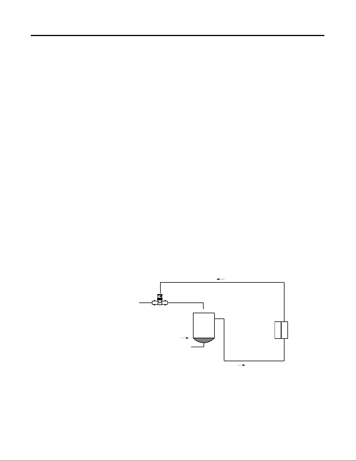
in many forms. The following application shows a typical use of analog data.
In this application, the processor controls the amount of fluid in a holding
tank by adjusting the valve opening. The valve is initially open 100%. As the
fluid level in the tank approaches the preset point, the processor modifies the
output to close the valve 90%, 80%, and so on, continuously adjusting the
valve to maintain the fluid level.
Figure 1.1 Analog I/O Application Example
Analog output
wired to valve
Valve
Controller
Level Sensor
Analog input wired
to tank
Analog I/O
Module
1 Publication 1769-UM002B-EN-P - July 2005
Page 16

1-2 Overview
General Description
The 1769-IF4 and -IF8 analog input modules convert and digitally store analog
data for retrieval by controllers, such as the CompactLogix™ or MicroLogix™
1500. The module supports connections from any combination of up to four
voltage or current analog sensors for the 1769-IF4 and up to eight for the
1769-IF8. The high-impedance input channels can be wired as either
single-ended or differential inputs.
The 1769-OF2 output module provides two single-ended analog output
channels, each individually configurable for voltage or current. The
1769-OF8C and -OF8V output modules each provide eight single-ended
analog output channels.
Both modules provide the following input/output types/ranges:
Table 1.1 Normal and Full Ranges
Normal Operating Input Range Full Module Range
±10V dc ± 10.5V dc
1 to 5V dc 0.5 - 5.25V dc
0 to 5V dc -0.5 - +5.25V dc
0 to 10V dc -0.5 - +10.5V dc
0 to 20 mA 0 - 21 mA
4 to 20 mA 3.2 - 21 mA
The data can be configured on board each module as:
• Engineering Units
• Scaled-for-PID
• Percent
• Raw/Proportional Data
Publication 1769-UM002B-EN-P - July 2005
Page 17
Overview 1-3
1
5
b
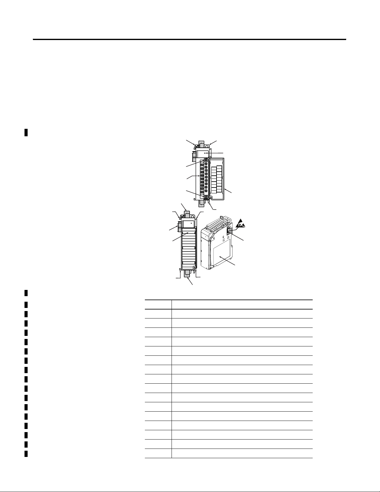
Hardware Features
The modules contain removable terminal blocks. The 1769-IF4 and -IF8
channels can be wired as either single-ended or differential inputs. The
1769-OF2, -OF8C, and -OF8V channels are single-ended only. Module
configuration is normally done via the controller’s programming software. In
addition, some controllers support configuration via the user program. In
either case, the module configuration is stored in the memory of the controller.
Refer to your controller’s user manual for more information.
Figure 1.2 1769-OF2, -OF8C, -OF8V and -IF4 Analog Module’s Hardware Features
2a
OK
Analog
10a
10
10b
8a
7a
a
7a
OK
Analog
9
DANGER
Do Not Remove RTB Under Power
Unless Area is Non-Hazardous
I out 0 +
I out 1 +
I out 2 +
I out 3 +
I out 4 +
I out 5 +
I out 6 +
I out 7 +
+24V dc
Ensure Adjacent
Bus Lever is Unlatched/Latched
Before/After
Removing/Inserting Module
1769-OF8C
2b
3
ANLG
Com
ANLG
Com
ANLG
Com
ANLG
Com
ANLG
Com
ANGL
Com
ANLG
Com
ANLG
Com
dc
NEUT
4
5
6
7b
7b
8b
Table 1.2 1769-OF2, -OF8C, -OF8V, and -IF4 Feature Descriptions
Item Description
1 bus lever (with locking function)
2a upper panel mounting tab
2b lower panel mounting tab
3 module status LEDs
4 module door with terminal identification label
5a movable bus connector with female pins
5b stationary bus connector with male pins
6 nameplate label
7a upper tongue-and-groove slots
7b lower tongue-and-groove slots
8a upper DIN rail latch
8b lower DIN rail latch
9 write-on label for user identification tags
10 removable terminal block (RTB) with finger-safe cover
10a RTB upper retaining screw
10b RTB lower retaining screw
Publication 1769-UM002B-EN-P - July 2005
Page 18
1-4 Overview
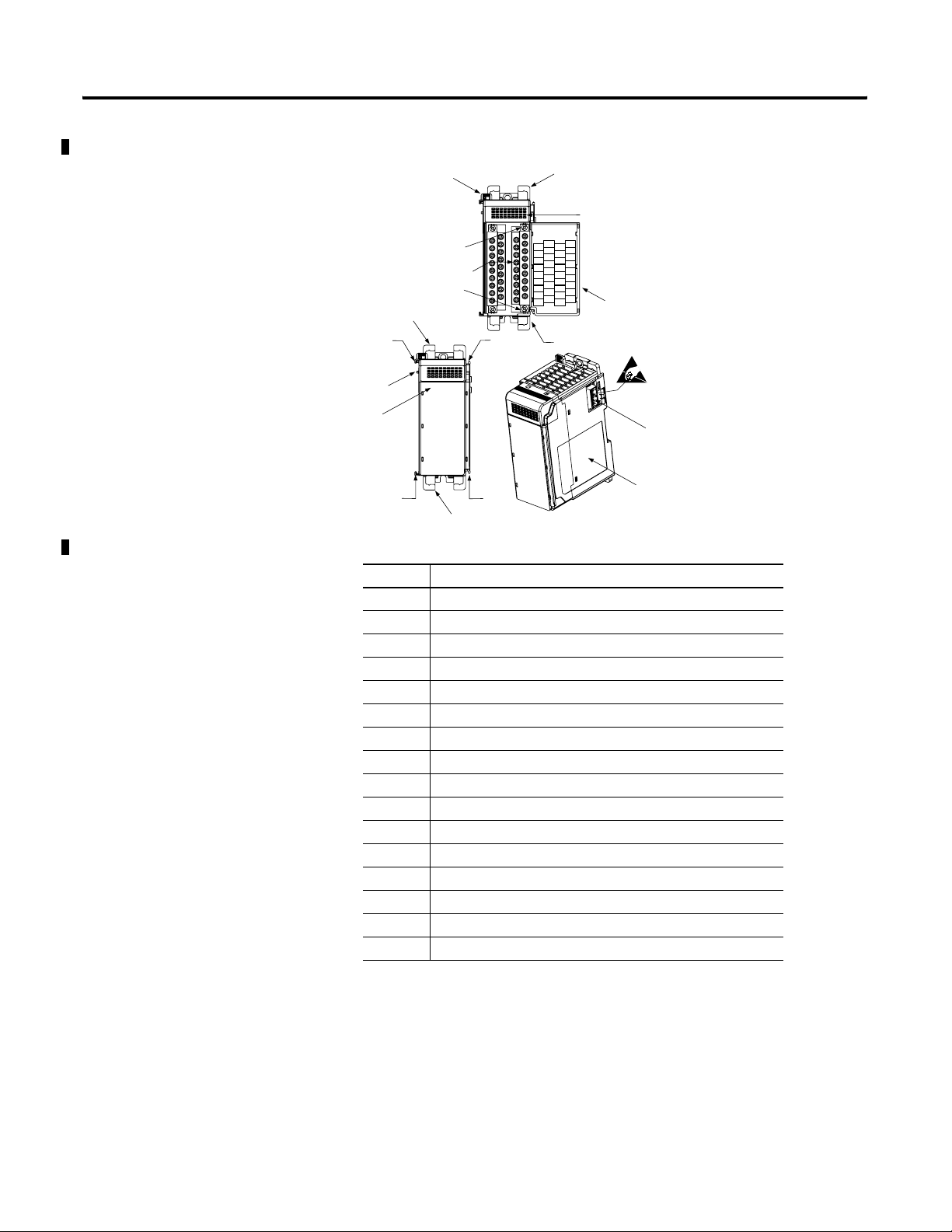
Figure 1.3 1769-IF8 Analog Module’s Hardware Features
IN 1
IN 3
IN 5
IN 7
IN 9
IN 11
IN 13
IN 15
DC COM
WARNING -Do Not
Remove RTB Unless
Area is Non-Hazardous
IN 0
IN 2
IN 4
IN 6
DC COM
IN 8
IN 10
IN 12
IN 14
DC COM
1769-IQ32
2a
3
IN 16
IN 17
IN 18
IN 19
IN 20
IN 21
IN 22
IN 23
DC COM
IN 25
IN 24
IN 27
IN 26
IN 29
IN 28
IN 31
IN 30
4
2b
1
10a
10
10b
8a
7a
7a
5a
9
5b
7b
7b
8b
6
30538-M
Table 1.3 1769-IF8 Feature Descriptions
Item Description
1 bus lever (with locking function)
2a upper panel mounting tab
2b lower panel mounting tab
3 I/O diagnostic LEDs
4 module door with terminal identification label
5a movable bus connector with female pins
5b stationary bus connector with male pins
6 nameplate label
7a upper tongue-and-groove slots
7b lower tongue-and-groove slots
8a upper DIN rail latch
8b lower DIN rail latch
9 write-on label for user identification tags
10 removable terminal block (RTB) with finger-safe cover
10a RTB upper retaining screw
10b RTB lower retaining screw
Publication 1769-UM002B-EN-P - July 2005
Page 19

Overview 1-5
General Diagnostic Features
The analog modules contain diagnostic features that can help you identify the
source of problems that may occur during power-up or during normal channel
operation. These power-up and channel diagnostics are explained in chapter 6,
Module Diagnostics and Troubleshooting.
System Overview
The modules communicate to the controller through the bus interface. The
modules also receive 5 and 24V dc power through the bus interface. The
1769-IF4, -OF2, -OF8C, and -OF8V modules feature an external 24V dc
power switch, providing you with the option of using an external power
supply. See External Power Switch on page 2-10 for details.
You can install as many analog modules as your power supply can support.
However, the modules have a power supply distance rating of 8, which means
that they may not be located more than 8 modules away from the system
power supply.
Figure 1.4 Determine Power Supply Distance
Adapter
Compact I/O
or I/O Communication
CompactLogix Controller
Compact I/O
Compact I/O
System Power Supply
Compact I/O
Compact I/O
1123432
OR
End Cap
Compact I/O
Power Supply Distance
MicroLogix 1500 Controller
with Integrated System
Power Supply
Compact I/O
Compact I/O
1
234
End Cap
Compact I/O
Compact I/O
Power Supply Distance
Publication 1769-UM002B-EN-P - July 2005
Page 20

1-6 Overview
System Operation
At power-up, the module performs a check of its internal circuits, memory,
and basic functions. During this time, the module status LED remains off. If
no faults are found during power-up diagnostics, the module status LED is
turned on.
After power-up checks are complete, the module waits for valid channel
configuration data. If an invalid configuration is detected, the module
generates a configuration error. Once a channel is properly configured and
enabled, it begins the analog-to-digital or digital-to-analog conversion process.
Input Modules
Each time a channel is read by the input modules, that analog data value is
tested by the modules for an over-range or under-range condition. If such a
condition is detected, a unique bit is set in the channel status word. The
channel status word is described in 1769-IF4 Input Data File on page 3-2 and
1769-IF8 Input Data File on page 3-18.
The controller reads the two’s complement binary converted analog data from
the modules. This typically occurs at the end of the program scan or when
commanded by the control program. If the controller and the modules
determine that the bus data transfer was made without error, the data is used in
your control program.
Output Modules
The output modules monitor channels for over-range and under-range
conditions and also for broken output wires and high load resistance (in
current mode only). If such a condition is detected, a unique bit is set in the
channel status word. The channel status word is described in 1769-OF2
Output Data File on page 4-2 and 1769-OF8C and -OF8V Output Data File
on page 4-18.
The output module receives two’s complement binary values from the bus
master. This typically occurs at the end of the program scan or when
commanded by the control program. If the controller and the module
determine that the bus transfer was completed without error, the output
module converts the data to an analog output signal.
Publication 1769-UM002B-EN-P - July 2005
Page 21
Input
Overview 1-7
Module Operation
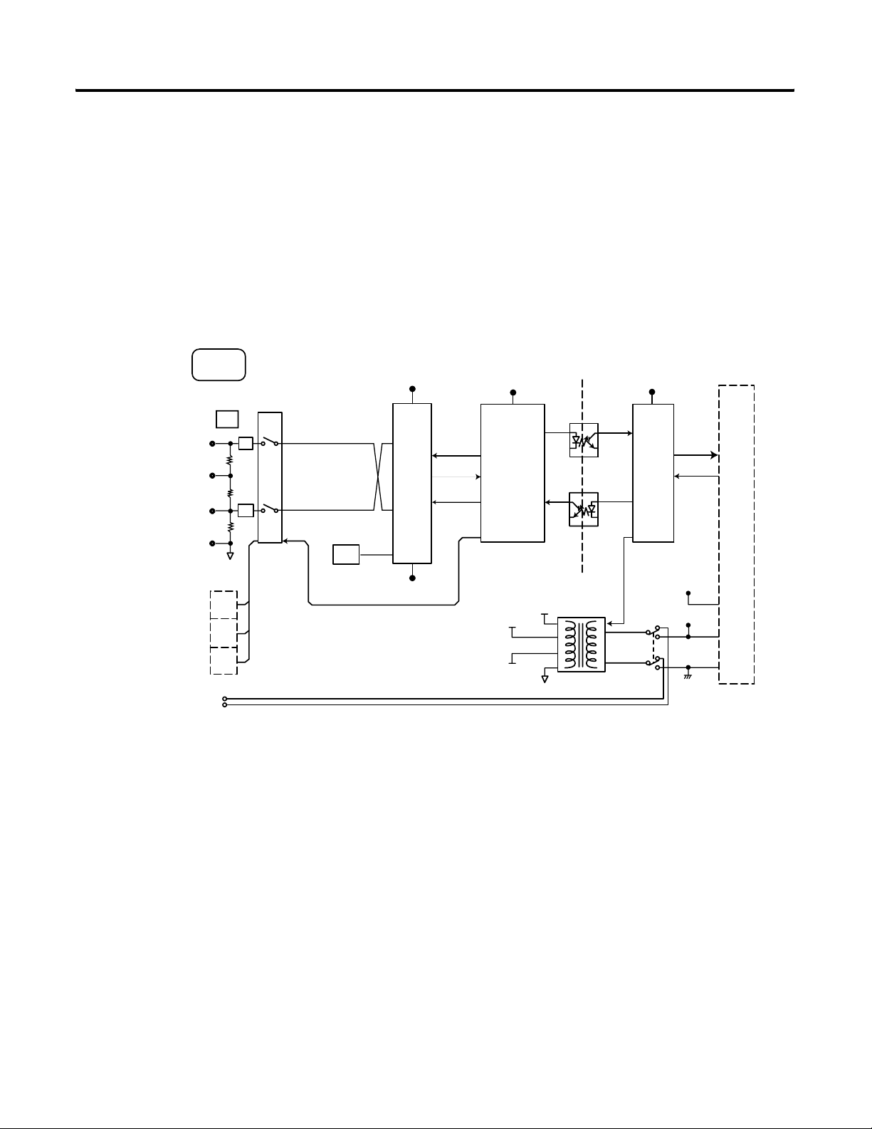
Input Module Block Diagram
The input module’s input circuitry consists of four differential analog inputs
multiplexed into a single analog-to-digital (A/D) converter. The
A/D converter reads the selected input signal and converts it to a digital value
which is presented to the controller. The multiplexer sequentially switches
each input channel to the module’s A/D converter.
Figure 1.5 1769-IF4 Block Diagram
Galvanic
VA2
VA1 VS1
Isolation
CH0
Vin+
Iin+
V/Iin-
COM
A-GND
CH1
CH2
CH3
dc Neutral
+24V dc
Multiplexer
(same as above)
Vref VREF
Channel Select
AIN+
A/D
AIN-
VA3
TXD
MCU ASIC
RXD
DC/DC
Power
VA1
VA2
VA3
Supply
A-GND S-GND
Bus
VS1
VS2
Publication 1769-UM002B-EN-P - July 2005
Page 22
1-8 Overview
Figure 1.6 1769-IF8 Block Diagram
CH0
CH1
CH2
CH3
CH4
CH5
CH6
CH7
Vin +
Iin +
V/ICom
Vin +
Iin +
V/ICom
Vin +
Iin +
V/ICom
Vin +
Iin +
V/ICom
Vin +
Iin +
V/ICom
Vin +
Iin +
V/ICom
Vin +
Iin +
V/ICom
Vin +
Iin +
V/ICom
Select
Select
High
Impedance
High
Impedance
Gain
Vref
Gain
AD
Converter
AD
Converter
EN0
A1
A0
EN1
EN1
CPU
Opto
Coupler
Opto
Coupler
Opto
Coupler
+15V
+5V
-15V
GND
ASIC
DC/DC
converter
LED
CN2
(Out)
+24V
GND
31542-M
CN1
(In)
Publication 1769-UM002B-EN-P - July 2005
Page 23

Output
Overview 1-9
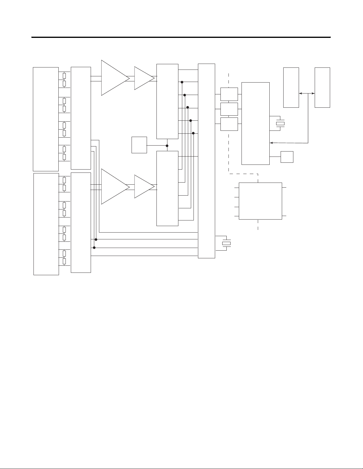
Output Module Block Diagram
The output module uses a digital-to-analog (D/A) converter to read the digital
output data from the controller and convert it to an analog output signal.
Figure 1.7 1769-OF2 Block Diagram
Galvanic
Isolation
VA2
VA1
VS1
CH0
Iout+
Vout+
COM
dc Neutral
+24V dc
A-GND
TXD
RXD
Power Supply
VA1
DC/DC
ASIC
VS1
VS2
A-GND
VA2
VA3
CH1
Analog Switch
Selec
Iout
D/A
Iout
Refout
Latch
Latch
Selec
MCU
VA2
(same as above)
VA3
A-GND S-GND
Figure 1.8 1769-OF8C and -OF8V Block Diagram
The following diagram shows only one of eight outputs. For each analog
output, only one of the sections shown in broken-line boxes is implemented.
The 1769-OF8C module uses only the Current Out section while the
1769-OF8V module uses only the Voltage Out section.
Bus
16 pin backplane connector
ASIC
+24 VDC
GND
Curent Out
OC
Detect
CFU
64K Flash/
2K RAM
JP
OPTOS
500VDC Isoleted
Power Supply
+5V
+15V -15V
GND
16 Bit
DAC
Voltage Out
+
-
ESD Limit
18 pin Terminal Block
EXT 24VDC
GND
Publication 1769-UM002B-EN-P - July 2005
Page 24

1-10 Overview
Module Field Calibration
The 1769-IF4 and -IF8 input modules performs autocalibration when a
channel is initially enabled. In addition, if a channel is configured differently
than the previously scanned channel, an autocalibration cycle is run as part of
the reconfiguration process.
The 1769-OF2, -OF8C, and -OF8V output modules’s calibration is
guaranteed by its design. No field calibration is required.
Publication 1769-UM002B-EN-P - July 2005
Page 25

Installation and Wiring
This chapter tells you how to:
• determine the power requirements for the modules
• avoid electrostatic damage
• install the module
• wire the module’s terminal block
• wire input devices
• wire output devices
Chapter
2
Compliance to European Union Directives
This product is approved for installation within the European Union and EEA
regions. It has been designed and tested to meet the following directives.
EMC Directive
The analog modules are tested to meet Council Directive 89/336/EEC
Electromagnetic Compatibility (EMC) and the following standards, in whole
or in part, documented in a technical construction file:
• EN 50081-2
EMC – Generic Emission Standard, Part 2 - Industrial Environment
• EN 50082-2
EMC – Generic Immunity Standard, Part 2 - Industrial Environment
This product is intended for use in an industrial environment.
Low Voltage Directive
This product is tested to meet Council Directive 73/23/EEC Low Voltage, by
applying the safety requirements of EN 61131-2 Programmable Controllers,
Part 2 – Equipment Requirements and Tests.
For specific information required by EN61131-2, see the appropriate sections
in this publication, as well as the following Allen-Bradley publications:
• Industrial Automation, Wiring and Grounding Guidelines for Noise Immunity,
publication 1770-4.1
• Automation Systems Catalog, publication B113
1 Publication 1769-UM002B-EN-P - July 2005
Page 26

2-2 Installation and Wiring
Power Requirements
General Considerations
The modules receive power through the bus interface from the +5V dc/+24V
dc system power supply. Some modules can also be supplied 24V dc power by
an external power supply connected to the module’s terminal block.
Table 2.1 Maximum Current Draw
Module 5V dc 24V dc
1769-IF4 (Series A)
1769-IF4 (Series B)
120 mA
Not applicable
(1)
60 mA
1769-IF8 (Series A) 70 mA
1769-OF2 (Series A) 120 mA Not applicable
1769-OF2 (Series B)
1769-OF8C (Series A)
145 mA
1769-OF8V (Series A)
(1)
If the optional 24V dc Class 2 power supply is used, the 24V dc current draw from the bus is 0 mA.
120 mA
160 mA
125 mA
(1)
(1)
(1)
Compact I/O is suitable for use in an industrial environment when installed in
accordance with these instructions. Specifically, this equipment is intended for
(1)
use in clean, dry environments (Pollution degree 2
exceeding Over Voltage Category II
(2)
(IEC 60664-1).
) and to circuits not
(3)
Publication 1769-UM002B-EN-P - July 2005
(1)
Pollution Degree 2 is an environment where, normally, only non-conductive pollution occurs except that
occasionally a temporary conductivity caused by condensation shall be expected.
(2)
Over Voltage Category II is the load level section of the electrical distribution system. At this level transient
voltages are controlled and do not exceed the impulse voltage capability of the product’s insulation.
(3)
Pollution Degree 2 and Over Voltage Category II are International Electrotechnical Commission (IEC)
designations.
Page 27

Installation and Wiring 2-3
Hazardous Location Considerations
This equipment is suitable for use in Class I, Division 2, Groups A, B, C, D or
non-hazardous locations only. The following WARNING statement applies to
use in hazardous locations.
ATTENTION
EXPLOSION HAZARD
• Substitution of components may impair suitability for
Class I, Division 2.
• Do not replace components or disconnect equipment
unless power has been switched off or the area is
known to be non-hazardous.
• Do not connect or disconnect components unless
power has been switched off or the area is known to be
non-hazardous.
• This product must be installed in an enclosure.
• All wiring must comply with N.E.C. article 501-4(b).
Prevent Electrostatic Discharge
ATTENTION
Electrostatic discharge can damage integrated circuits or
semiconductors if you touch analog I/O module bus
connector pins or the terminal block on the input module.
Follow these guidelines when you handle the module:
• Touch a grounded object to discharge static potential.
• Wear an approved wrist-strap grounding device.
• Do not touch the bus connector or connector pins.
• Do not touch circuit components inside the module.
• If available, use a static-safe work station.
• When it is not in use, keep the module in its
static-shield box.
Publication 1769-UM002B-EN-P - July 2005
Page 28

2-4 Installation and Wiring
Remove Power
ATTENTION
Remove power before removing or inserting this module.
When you remove or insert a module with power applied,
an electrical arc may occur. An electrical arc can cause
personal injury or property damage by:
• sending an erroneous signal to your system’s field
devices, causing unintended machine motion
• causing an explosion in a hazardous environment
• Electrical arcing causes excessive wear to contacts on
both the module and its mating connector and may lead
to premature failure.
Reducing Noise
Most applications require installation in an industrial enclosure to reduce the
effects of electrical interference. Analog inputs and outputs are highly
susceptible to electrical noise. Electrical noise coupled to the analog inputs will
reduce the performance (accuracy) of the module.
Group your modules to minimize adverse effects from radiated electrical noise
and heat. Consider the following conditions when selecting a location for the
analog module. Position the module:
System Assembly
• away from sources of electrical noise such as hard-contact switches,
relays, and AC motor drives
• away from modules which generate significant radiated heat, such as the
1769-IA16. Refer to the module’s heat dissipation specification.
In addition, route shielded, twisted-pair analog input and output wiring away
from any high voltage I/O wiring.
Protecting the Circuit Board from Contamination
The printed circuit boards of the analog modules must be protected from dirt,
oil, moisture, and other airborne contaminants. To protect these boards, the
system must be installed in an enclosure suitable for the environment. The
interior of the enclosure should be kept clean and the enclosure door should
be kept closed whenever possible.
The module can be attached to the controller or an adjacent I/O module before
or after mounting. For mounting instructions, see Panel Mounting Using the
Dimensional Template on page 2-7, or DIN Rail Mounting on page 2-8. To
Publication 1769-UM002B-EN-P - July 2005
Page 29
Installation and Wiring 2-5
work with a system that is already mounted, see Replacing a Single Module
within a System on page 2-9.
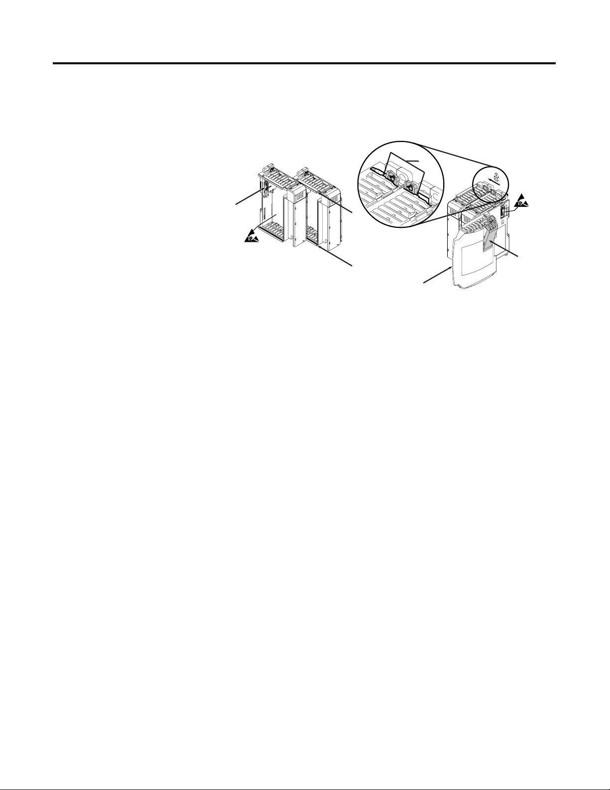
Figure 2.1 Assemble the Compact I/O System
3
4
2
1
6
1
5
1. Disconnect power.
2. Check that the bus lever of the module to be installed is in the unlocked
(fully right) position.
3. Use the upper and lower tongue-and-groove slots (1) to secure the
modules together (or to a controller).
4. Move the module back along the tongue-and-groove slots until the bus
connectors (2) line up with each other.
5. Push the bus lever back slightly to clear the positioning tab (3). Use your
fingers or a small screwdriver.
Publication 1769-UM002B-EN-P - July 2005
Page 30
2-6 Installation and Wiring
6. To allow communication between the controller and module, move the
bus lever fully to the left (4) until it clicks. Ensure it is locked firmly in
place.
Mounting
ATTENTION
When attaching I/O modules, it is very important
that the bus connectors are securely locked together
to ensure proper electrical connection.
7. Attach an end cap terminator (5) to the last module in the system by
using the tongue-and-groove slots as before.
8. Lock the end cap bus terminator (6).
IMPORTANT
A 1769-ECR or 1769-ECL right or left end cap must be
used to terminate the end of the bus.
ATTENTION
During panel or DIN rail mounting of all devices, be sure
that all debris (metal chips, wire strands, etc.) is kept from
falling into the module. Debris that falls into the module
could cause damage at power up.
Publication 1769-UM002B-EN-P - July 2005
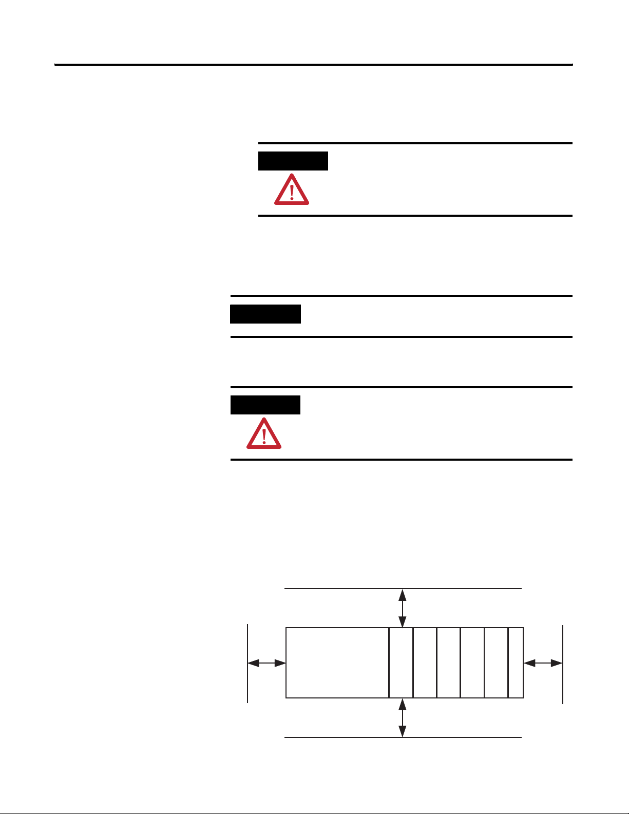
Minimum Spacing
Maintain spacing from enclosure walls, wireways, adjacent equipment, etc.
Allow 50 mm (2 in.) of space on all sides for adequate ventilation.
Figure 2.2 Space Requirements
Top
Side Side
Host Controller
Compact I/O
Bottom
Compact I/O
Compact I/O
Compact I/O
End Cap
Compact I/O
Page 31

Installation and Wiring 2-7
Panel Mounting
Mount the module to a panel using two screws per module. Use M4 or #8 panhead screws. Mounting screws are required on every module.
Figure 2.3 Panel Mounting Using the Dimensional Template
For more than 2 modules: (number of modules-1) X 35 mm (1,38 in.).
Refer to host controller documentation for this dimension.
132
(5.197)
35
(1.38)
28.5
(1.12)
122.6±0.2
(4.826±0.008)
NOTE: All dimensions are in mm (inches).
Hole spacing tolerance: ±0.04 mm (0.016 in.).
Host Controller
Figure 2.4 Panel Mounting for the 1769-IF8 Using the Dimensional Template
Spacing for one-and-a-half-wide modules 52.5 mm (2.067 in).
Spacing for single-wide modules 35 mm (1.378 in).
Refer to host controller documentation for this dimension.
NOTE: Overall hole spacing
tolerance: ±0.4 mm (0.016 in.)
Locate holes every 17.5 mm (0.689 in) to allow for a
mix of single-wide and one-and-a-half-wide modules
(e.g., 1769-OA16).
l Mounting
Host Controller
Compact I/O
Compact I/O
Compact I/O
Right End Cap
Publication 1769-UM002B-EN-P - July 2005
Page 32

2-8 Installation and Wiring
Panel Mounting Procedure Using Modules as a Template
The following procedure allows you to use the assembled modules as a
template for drilling holes in the panel. If you have sophisticated panel
mounting equipment, you can use the dimensional template provided on
page 2-7. Due to module mounting hole tolerance, it is important to follow
these procedures:
1. On a clean work surface, assemble no more than three modules.
2. Using the assembled modules as a template, carefully mark the center of
all module-mounting holes on the panel.
3. Return the assembled modules to the clean work surface, including any
previously mounted modules.
4. Drill and tap the mounting holes for the recommended M4 or #8 screw.
5. Place the modules back on the panel, and check for proper hole
alignment.
6. Attach the modules to the panel using the mounting screws.
TIP
7. Repeat steps 1 to 6 for any remaining modules.
If mounting more modules, mount only the last one of this
group and put the others aside. This reduces remounting
time during drilling and tapping of the next group.
DIN Rail Mounting
The module can be mounted using the following DIN rails:
35 x 7.5 mm (EN 50 022 - 35 x 7.5) or 35 x 15 mm (EN 50 022 - 35 x 15).
Before mounting the module on a DIN rail, close the DIN rail latches. Press
the DIN rail mounting area of the module against the DIN rail. The latches
will momentarily open and lock into place.
Publication 1769-UM002B-EN-P - July 2005
Page 33

Installation and Wiring 2-9
Replacing a Single Module
The module can be replaced while the system is mounted to a panel (or DIN
rail). Follow these steps in order:
within a System
1. Remove power. See important note on 2-4.
2. On the module to be removed, remove the upper and lower mounting
screws from the module (or open the DIN latches using a flat-blade or
phillips-style screwdriver).
3. Move the bus lever to the right to disconnect (unlock) the bus.
4. On the right-side adjacent module, move its bus lever to the right
(unlock) to disconnect it from the module to be removed.
5. Gently slide the disconnected module forward. If you feel excessive
resistance, check that the module has been disconnected from the bus,
and that both mounting screws have been removed (or DIN latches
opened).
TIP
It may be necessary to rock the module slightly from front
to back to remove it, or, in a panel-mounted system, to
loosen the screws of adjacent modules.
6. Before installing the replacement module, be sure that the bus lever on
the module to be installed and on the right-side adjacent module are in
the unlocked (fully right) position.
7. Slide the replacement module into the open slot.
8. Connect the modules together by locking (fully left) the bus levers on
the replacement module and the right-side adjacent module.
9. Replace the mounting screws (or snap the module onto the DIN rail).
Publication 1769-UM002B-EN-P - July 2005
Page 34

2-10 Installation and Wiring
External Power Switch
External Power
Supply Switch
Bus Power (default)
External Power
The analog modules have an external 24V dc power switch which gives you
the option of using an external power supply. The switch is located in on the
lower left portion of the module’s circuit board, as shown below. With the
switch pressed on the top (default), 24V dc power is drawn from the 1769
system power supply via the 1769 I/O bus. Pressed on the bottom, 24V dc
power is drawn from the external power supply.
Wire the external power supply to the module via the module’s terminal block.
The external power supply must be Class 2 rated, with a 24V dc range of 20.4
to 26.4V dc and a minimum current rating that meets the needs of the modules
used in your application. Refer to Maximum Current Draw on page 2-2.
IMPORTANT
Only 1769-IF4 and -OF2 Series B modules have the 24V
dc power switch.
Figure 2.5 External Power Switch
1769-IF4 and -OF2 Modules 1769-OF8C and -OF8V Modules
External Power Switch
Pressed on the Top
Bus Power (default)
Pressed on the Bottom
External Power
BUS EXT
Field Wiring Connections
Publication 1769-UM002B-EN-P - July 2005
Grounding
This product is intended to be mounted to a well-grounded mounting surface
such as a metal panel. Additional grounding connections from the module’s
mounting tabs or DIN rail (if used) are not required unless the mounting
surface cannot be grounded. Refer to Industrial Automation Wiring and Grounding
Guidelines, Allen-Bradley publication 1770-4.1, for additional information.
Page 35

Installation and Wiring 2-11
System Wiring Guidelines
Consider the following when wiring your system:
General
• All module commons (ANLG COM) are connected in the analog
module. The analog common (ANLG COM) is not connected to earth
ground inside the module.
• Channels are not isolated from each other.
• Do not use the analog module’s NC terminals as connection points.
• To ensure optimum accuracy, limit overall cable impedance by keeping
your cable as short as possible. Locate the I/O system as close to your
sensors or actuators as your application will permit.
• Use Belden™ 8761, or equivalent, shielded wire.
• Keep shield connection to ground as short as possible.
• Under normal conditions, the drain wire and shield junction must be
connected to earth ground via a panel or DIN rail mounting screw at
the analog I/O module end.
(1)
1769-IF4 and -IF8 Input Modules
• If multiple power supplies are used with analog inputs, the power supply
commons must be connected together.
• The 1769-IF4 and -IF8 modules do not provide loop power for analog
inputs. Use a power supply that matches the input transmitter
specifications.
• Differential analog inputs are more immune to noise than single-ended
analog inputs.
• Voltages on Vin+, V/Iin-, and Iin+ of the 1769-IF4 and -IF8 modules
must be within ±10V dc of analog common.
1769-OF2, -OF8C, and -OF8V Output Modules
• Voltage outputs (Vout 0+ and Vout 1+ for 1769-OF2, Vout 0+
through Vout 7+ for 1769-OF8V) of the output modules are referenced
to ANLG COM. Load resistance for a voltage output channel must be
equal to or greater than 1K Ω.
• Current outputs (Iout 0+ and Iout 1+ for 1769-OF2, Iout 0+ through
Iout 7+ for 1769-OF8C) of the output modules source current that
returns to ANLG COM. Load resistance for a current output channel
must remain between 0 and 500 Ω.
(1)
In environments where high-frequency noise may be present, it may be necessary to directly ground cable
shields to earth at the module end and via a 0.1µF capacitor at the sensor end.
Publication 1769-UM002B-EN-P - July 2005
Page 36

2-12 Installation and Wiring
Effect of Transducer/Sensor and Cable Length Impedance on Voltage Input Accuracy
For voltage inputs, the length of the cable used between the transducer/sensor
and the 1769-IF4 or -IF8 module can affect the accuracy of the data provided
by the module.
Figure 2.6 Voltage Input Accuracy
RcRs
+
Ri
Where:
Vs
V in
-
Rc
Rc = DC resistance of the cable (each conductor) depending on
cable length
Rs = Source impedance of analog transducer/sensor input
Ri = Impedance of the voltage input
(220 KΩ for 1769-IF4 and -IF8)
Vs = Voltage source
(voltage at the transducer/sensor input device)
Vin = Measured potential at the module input
%Ai = Percent added inaccuracy in a voltage-based system due
to source and cable impedance.
Vin
Rs 2 Rc×()Ri++[]
Ri Vs×[]
-------------------------------------------------------
=
For example, for Belden 8761 two conductor, shielded cable:
Rc = 16 Ω/1000 ft
Rs = 0 (ideal
%Ai 1
Vin
⎛⎞
---------
∠
⎝⎠
Vs
100×=
source)
Publication 1769-UM002B-EN-P - July 2005
Page 37

Table 2.2 Effect of Cable Length on Input Accuracy
Installation and Wiring 2-13
Length of Cable (m) dc resistance of the cable,
Rc (Ω)
50 2.625 0.00238%
100 5.25 0.00477%
200 10.50 0.00954%
300 15.75 0.0143%
Accuracy impact at the
input module
As input source impedance (Rs) and/or resistance (dc) of the cable (Rc) get
larger, system accuracy decreases. If you determine that the inaccuracy error is
significant, implementing the following equation in the control program can
compensate for the added inaccuracy error due to the impedance of the source
and cable.
Rs 2 Rc×()Ri++[]
-------------------------------------------------------
×=
Ri
TIP
Vs Vin
In a current loop system, source and cable impedance do
not impact system accuracy.
Effect of Device and Cable Output Impedance on Output Module Accuracy
The maximum value of the output impedance is shown in the example below,
because it creates the largest deviation from an ideal voltage source.
Figure 2.7 Output Module Accuracy
+
Vs
-
Where:
Rc = DC resistance of the cable (each conductor)
depending on cable length
Rs = Source impedance
(15 Ω for 1769-OF2 and 1 Ω for 1769-OF8V)
Ri = Impedance of the voltage input
(220 KΩ for 1769-IF4)
Vs = Voltage at the output of 1769-OF2
Vin = Measured potential at the module input
%Ai = Percent added inaccuracy in a voltage-based
system due to source and cable impedance.
Vin
Ri Vs×[]
-------------------------------------------------------=
Rs 2 Rc×()Ri++[]
RcRs
V in
Rc
Ri
Publication 1769-UM002B-EN-P - July 2005
Page 38

2-14 Installation and Wiring
For example, for Belden 8761 two conductor, shielded cable and a 1769-IF4
input module:
Rc = 16 Ω/1000 ft
Rs = 15 Ω
%Ai 1
Vin
⎛⎞
---------
∠
⎝⎠
Vs
100×=
Ri = 220 KΩ
Table 2.3 Effect of Output Impedance and Cable Length on Accuracy
Length of Cable (m) dc resistance of the cable
Rc (Ω)
50 2.625 0.00919%
100 5.25 0.01157%
200 10.50 0.01634%
300 15.75 0.02111%
Accuracy impact at the
input module
As output impedance (Rs) and/or resistance (dc) of the cable (Rc) get larger,
system accuracy decreases. If you determine that the inaccuracy error is
significant, implementing the following equation in the control program can
compensate for the added inaccuracy error due to the impedance of the output
module and cable.
Rs 2 Rc×()Ri++[]
-------------------------------------------------------
×=
Ri
TIP
Vs Vin
In a current loop system, source and cable impedance do
not impact system accuracy.
Publication 1769-UM002B-EN-P - July 2005
Page 39

Installation and Wiring 2-15
Labeling the Terminals
A removable, write-on label is provided with the module. Remove the label
from the door, mark the identification of each terminal with permanent ink,
and slide the label back into the door. Your markings (ID tag) will be visible
when the module door is closed.
Figure 2.8 Terminal Labels
upper retaining screw
lower retaining screw
wiring the
finger-safe
terminal block
Removing the Finger-Safe Terminal Block
When wiring field devices to the module, it is not necessary to remove the
terminal block. If you remove the terminal block, use the write-on label on the
side of the terminal block to identify the module slot location and type. RTB
position can be indicated by circling either the ‘R’ for right side or ‘L’ for left
side.
Figure 2.9 Finger-Safe Terminal Block
SLOT # _____
MODULE TYPE ______
To remove the terminal block, loosen the upper and lower retaining screws.
The terminal block will back away from the module as you remove the screws.
When replacing the terminal block, torque the retaining screws to 0.46 Nm
(4.1 in-lbs).
Publication 1769-UM002B-EN-P - July 2005
Page 40

2-16 Installation and Wiring
Wiring the Finger-Safe Terminal Block
When wiring the terminal block, keep the finger-safe cover in place.
1. Loosen the terminal screws to be wired.
2. Begin wiring at the bottom of the terminal block and move up.
3. Route the wire under the terminal pressure plate. You can use the bare
wire or a spade lug. The terminals accept a 6.35 mm (0.25 in.) spade lug.
TIP
The terminal screws are non-captive. Therefore, it is
possible to use a ring lug [maximum 1/4 inch o.d. with a
0.139 inch minimum i.d. (M3.5)] with the module.
4. Tighten the terminal screw making sure the pressure plate secures the
wire. Recommended torque when tightening terminal screws is 0.68 Nm
(6 in-lbs).
TIP
If you need to remove the finger-safe cover, insert a
screwdriver into one of the square, wiring holes and gently
pry the cover off. If you wire the terminal block with the
finger-safe cover removed, you will not be able to put it
back on the terminal block because the wires will be in the
way.
Wire Size and Terminal Screw Torque
Each terminal accepts up to two wires.
Table 2.4 Terminal Wire Considerations
Publication 1769-UM002B-EN-P - July 2005
Wire Type Wire Size Terminal Screw
Torque
Solid Cu-90°C (194°F) #14 to #22 AWG 0.68 Nm (6 in-lbs) 0.46 Nm (4.1 in-lbs)
Stranded Cu-90°C (194°F) #16 to #22 AWG 0.68 Nm (6 in-lbs) 0.46 Nm (4.1 in-lbs)
Retaining Screw
Torque
Page 41

Wiring the Modules
Installation and Wiring 2-17
ATTENTION
To prevent shock hazard, care should be taken when wiring
the module to analog signal sources. Before wiring any
analog module, disconnect power from the system power
supply and from any other source to the analog module.
After the analog module is properly installed, follow the wiring procedure
below. To ensure proper operation and high immunity to electrical noise,
always use Belden™ 8761 (shielded, twisted-pair) or equivalent wire.
ATTENTION
When wiring an analog input, take care to avoid connecting
a voltage source to a channel configured for current input.
Improper module operation or damage to the voltage
source can occur.
Never connect a voltage or current source to an analog
output channel.
Figure 2.10 Belden 8761 Wire
cable
Cut foil shield
and drain wire
signal wire
signal wire
drain wire
foil shield
signal wire
signal wire
Publication 1769-UM002B-EN-P - July 2005
Page 42

2-18 Installation and Wiring
To wire your module follow these steps.
1. At each end of the cable, strip some casing to expose the individual
wires.
2. Trim the signal wires to 2-inch lengths. Strip about 3/16 inch (5 mm) of
insulation away to expose the end of the wire.
ATTENTION
Be careful when stripping wires. Wire fragments that
fall into a module could cause damage at power up.
3. At one end of the cable, twist the drain wire and foil shield together.
Under normal conditions, this drain wire and shield junction must be
connected to earth ground, via a panel or DIN rail mounting screw at
the analog I/O module end. Keep the length of the drain wire as short
as possible.
In environments where high frequency noise may be present, it may be
necessary to ground the cable shields to earth at the module end via a
0.1 µF capacitor at the sensor end for analog inputs and at the load end
for analog outputs.
4. At the other end of the cable, cut the drain wire and foil shield back to
the cable.
5. Connect the signal wires to the terminal block as shown in Analog Input
Modules Wiring on page 2-19 and Analog Output Modules Wiring on
page 2-24. Connect the other end of the cable to the analog input or
output device.
Publication 1769-UM002B-EN-P - July 2005
6. Repeat steps 1 through 5 for each channel on the module.
Terminal Door Label
A removable, write-on label is provided with the module. Remove the label
from the door, mark the identification of each terminal with permanent ink,
and slide the label back into the door. Your markings (ID tag) will be visible
when the module door is closed.
Page 43

Installation and Wiring 2-19
Analog Input Modules Wiring
Figure 2.11 1769-IF4 Terminal Layout
DANGER
Do Not Remove RTB Under Power
Unless Area is Non-Hazardous.
+24V dc
Analog
Source
(optional)
V in 0 +
I in 0+
V in 1 +
I in 1+
V in 2 +
I in 2+
V in 3 +
I in 3+
1769-IF4
(2)
V/I in 0 -
ANLG Com
V/I in 1 -
ANLG Com
V/I in 2 -
ANLG Com
V/I in 3 -
ANLG Com
dc NEUT
V in 0 +
I in 0 +
V in 1 +
I in 1 +
V in 2 +
I in 2 +
V in 3 +
I in 3 +
+24V dc
V/I in 0 -
ANLG
Com
V/I in 1 -
ANLG
Com
V/I in 2 -
ANLG
Com
V/I in 3 -
ANLG
Com
dc NEUT
Ensure Adjacent Bus Lever is
Unlatched/Latched Before/After
Removing/Inserting Module
Figure 2.12 1769-IF4 Wiring Diagram Showing Differential Inputs
Belden 8761 cable (or equivalent)
1769-IF4
V/I in 0 -
ANLG Com
V/I in 1 -
ANLG Com
V/I in 2 -
ANLG Com
V/I in 3 -
ANLG Com
dc NEUT
V in 0 +
I in 0+
V in 1 +
I in 1+
V in 2 +
I in 2+
V in 3 +
I in 3+
+24V dc
earth ground
shield locally at
the module
External 24V dc
+
Power Supply
-
–
+
(1)
(1) The external power supply must be rated Class 2, with a 24V dc range of 20.4 to 26.4V dc and 60 mA minimum
for a single input module.
(2 ) Series B and later modules provide this option.
Publication 1769-UM002B-EN-P - July 2005
Page 44

2-20 Installation and Wiring
Figure 2.13 1769-IF4 Wiring Single-ended Sensor/Transmitter Types
1769-IF4 Terminal Block
Sensor/
Transmitter
Supply
+
-
+
+
+
External 24V dc
Power Supply
(optional)
(2)
Current
Transmitter
Signal
Voltage
Tra ns mi tt er
Ground
Voltage
Transmitter
Ground
(1)
+
-
Signal
Signal
V in 0 +
V/I in 0 -
I in 0 +
ANLG Com
V in 1 +
V/I in 1 -
I in 1 +
ANLG Com
V in 2 +
V/I in 2 -
I in 2 +
ANLG Com
V in 3 +
V/I in 3 -
I in 3 +
ANLG Com
+24V dc
dc NEUT
(1) The external power supply must be rated Class 2, with a 24V dc range of 20.4 to 26.4V dc and 60 mA minimum
for a single input module.
(2 ) Series B and later modules provide this option.
Publication 1769-UM002B-EN-P - July 2005
Page 45

Figure 2.14 1769-IF4 Wiring Mixed Transmitter Types
Single-ended
Voltage
Transmitter
–
Differential
Voltage
Transmitter
–
Supply
Differential
Current
Transmitter
–
Supply
2-Wire Current
Transmitter
Signal
+
+
Signal
–
+
–
Signal
+
+
Signal
+
Installation and Wiring 2-21
1769-IF4 Terminal Block
V in 0 +
V/I in 0 -
I in 0 +
ANLG Com
V in 1 +
V/I in 1 -
I in 1 +
ANLG Com
V in 2 +
V/I in 2 -
I in 2 +
ANLG Com
V in 3 +
V/I in 3 -
I in 3 +
ANLG Com
+24V dc
dc NEUT
Sensor/Transmi
tter Supply
+
–
External 24V dc
Power Supply
(optional)
(1) The external power supply must be rated Class 2, with a 24V dc range of 20.4 to 26.4V dc and 60 mA minimum
for a single input module.
(2) Series B and later modules provide this option.
(1)
+
–
Publication 1769-UM002B-EN-P - July 2005
Page 46

2-22 Installation and Wiring
N
A
V
A
V
A
V
A
V
+
–
–
Figure 2.15 1769-IF8 Terminal Layout
/I in 0-
NLG Com
/I in 1-
NLG Com
/I in 2-
NLG Com
/I in 3-
NLG Com
C
V in 0+
I in 0
V in 1+
I in 1
V in 2+
I in 2
V in 3+
I in 3
NC
V/I in 4-
ANLG Com
V/I in 5-
ANLG Com
V/I in 6-
ANLG Com
V/I in 7-
ANLG Com
NC
V in 4+
I in 4
V in 5+
I in 5
V in 6+
I in 6
V in 7+
I in 7
NC
Figure 2.16 1769-IF8 Wiring Differential Inputs
Belden 8761 cable (or equivalent)
WARNING -Do Not
Remove RTB Unless
Area is Non-Hazardous
V in 0+
V/I in 0-
ANLG Com
I in 0+
V in 1+
V/I in 1-
I in 1+
ANLG Com
V in 2+
V/I in 2-
I in 2+
ANLG Com
V in 3+
V/I in 3-
I in 3+
ANLG Com
NC
NC
analog source
V/I in 4-
ANLG Com
V/I in 5-
ANLG Com
V/I in 6-
ANLG Com
V/I in 7-
ANLG Com
NC
V in 4+
I in 4+
V in 5+
I in 5+
V in 6+
I in 6+
V in 7+
I in 7+
NC
1769-IF8
V/I in 0-
ANLG Com
V/I in 1-
ANLG Com
V/I in 2-
ANLG Com
V/I in 3-
ANLG Com
NC
V in 0+
I in 0+
V in 1+
I in 1+
V in 2+
I in 2+
V in 3+
I in 3+
NC
+
earth ground the
shield locally at
the module
V/I in 4-
ANLG Com
V/I in 5-
ANLG Com
V/I in 6-
ANLG Com
V/I in 7-
ANLG Com
NC
V in 4+
I in 4+
V in 5+
I in 5+
V in 6+
I in 6+
V in 7+
I in 7+
NC
Publication 1769-UM002B-EN-P - July 2005
Page 47

Installation and Wiring 2-23
–
–
Figure 2.17 1769-IF8 Wiring Single-Ended Sensor/Transmitter Types
Sensor/Tran
smitter
Supply
+
-
(1)
Current
Transmitter
+
Signal
Voltage
Transmitter
+
Ground
Voltage
Transmitter
+
Ground
Signal
Signal
(1) The external power supply must be rated Class 2, with a 24V dc range of 20.4 to 26.4V dc and 60 mA minimum
for a single input module.
1769-IF8 Terminal Block
V in 0 +
in
0
-
V/I
I in 0 +
AN
LG
C
o
m
V in 1 +
in
1
-
V/I
I in 1 +
AN
LG
C
o
m
V in 2 +
V/I in 2
-
I in 2 +
AN
LG
C
o
m
V in 3 +
V/I
in
3
-
I in 3 +
AN
LG
C
o
m
NC
NC
Wiring for channels 4-7 are identical.
Figure 2.18 1769-IF8 Wiring Mixed Transmitter Types
Single-ended
Voltage
Transmitter
+
–
Differential
Voltage
Transmitter
Supply
Differential
Current
Transmitter
Supply
2-Wire
Current
Transmitter
(1)
+
+
Signal
Signal
+
–
–
Signal
+
Signal
+
1769-IF8 Terminal Block
V in 0 +
V/I in 0 I in 0 +
ANLG Com
V in 1 +
V/I in 1 I in 1 +
ANLG Com
V in 2 +
V/I in 2 I in 2 +
ANLG Com
V in 3 +
V/I in 3 I in 3 +
ANLG Com
NC
NC
Sensor/
Transmitter
Supply
+
–
Wiring for channels 4-7 are identical.
(1) The external power supply must be rated Class 2, with a 24V dc range of 20.4 to 26.4V dc and 60 mA minimum
for a single input module.
Publication 1769-UM002B-EN-P - July 2005
Page 48

2-24 Installation and Wiring
Analog Output Modules Wiring
Figure 2.19 1769-OF2 Terminal Layout
I out 0 +
NC
I out 1 +
NC
dc Neutral
Figure 2.20 1769-OF2 Wiring Diagram
V out 0 +
ANLG Com
V out 1 +
ANLG Com
+24V dc
DANGER
Do Not Remove RTB Under Power
Unless Area is Non-Hazardous.
V in 0 -
ANLG
Com 0
V in 0 +
I in 0
V out 0 +
I out 0 +
ANLG Com
NC
V out 1 +
I out 1 +
ANLG Com
NC
+24V dc
dc NEUT
NC
I in 3
NC
1769-OF2
ANLG
Com 3
Ensure Adjacent Bus Lever is
Unlatched/Latched Before/After
Removing/Inserting Module
1769-OF2 Terminal Block
V out 0 +
Voltage Load
earth ground
Current Load
earth ground
External 24V dc
Power Supply
(optional)
(1) The external power supply must be rated Class 2, with a 24V dc range of 20.4 to 26.4V dc and 120 mA minimum
per output module.
(1)
+
-
I out 0 +
ANLG Com
NC
V out 1 +
I out 1 +
ANLG Com
NC
+24V dc
dc NEUT
Publication 1769-UM002B-EN-P - July 2005
Page 49

Figure 2.21 1769-OF8C Terminal Layout
+
I out 0+
I out 1+
I out 2+
I out 3+
I out 4+
I out 5+
I out 6+
I out 7+
24V dc
ANLG Com
ANLG Com
ANLG Com
ANLG Com
ANLG Com
ANLG Com
ANLG Com
ANLG Com
dc NEUT
Figure 2.22 1769-OF8C Wiring Diagram
Installation and Wiring 2-25
DANGER
Do Not Remove RTB Under Power
Unless Area is Non-Hazardous.
I
ou
ou
I
I
ou
ou
I
I
ou
I
ou
I
ou
I
ou
+24V
+
24v
Ensure Adjacent Bus Lever is
Unlatched/Latched Before/After
Removing/Inserting Module
t
t
t
t
t
t
t
t
0+
1+
2+
3+
4+
5+
6+
7+
d
d
c
c
AN
C
o
AN
C
o
AN
C
o
AN
C
o
AN
C
o
AN
C
o
AN
C
o
AN
C
o
d
c
NEUT
1769-OF
LG
m
LG
m
LG
m
LG
m
LG
m
LG
m
LG
m
LG
m
8C
ANLG Com
ANLG Com
ANLG Com
ANLG Com
ANLG Com
ANLG Com
ANLG Com
ANLG Com
dc NEUT
Current Load
External 24V dc Power
Supply (optional)(1)
earth ground
+
-
I out 0+
I out 1+
I out 2+
I out 3+
I out 4+
I out 5+
I out 6+
I out 7+
+24V dc
(1) The external power supply must be rated Class 2, with a 24V dc range of 20.4 to 26.4V dc and 120 mA minimum
per output module.
Publication 1769-UM002B-EN-P - July 2005
Page 50

2-26 Installation and Wiring
+
Figure 2.23 1769-OF8V Terminal Layout
V out 0+
V out 1+
V out 2+
V out 3+
V out 4+
V out 5+
V out 6+
V out 7+
24V dc
ANLG Com
ANLG Com
ANLG Com
ANLG Com
ANLG Com
ANLG Com
ANLG Com
ANLG Com
dc NEUT
Figure 2.24 1769-OF8V Wiring Diagram
DANGER
Do Not Remove RTB Under Power
Unless Area is Non-Hazardous.
V
ou
ou
V
V
ou
V
ou
V
ou
V
ou
V
ou
ou
V
+24V
+
24v
Ensure Adjacent Bus Lever is
Unlatched/Latched Before/After
Removing/Inserting Module
t
0+
t
1+
t
2+
t
3+
t
4+
t
5+
t
6+
t
7+
AN
LG
C
o
m
AN
LG
C
o
m
AN
LG
C
o
m
AN
LG
C
o
m
AN
LG
C
o
m
AN
LG
C
o
m
AN
LG
C
o
m
AN
LG
C
o
m
d
c
NEUT
d
c
d
c
1769-OF8V
ANLG Com
ANLG Com
ANLG Com
ANLG Com
ANLG Com
ANLG Com
ANLG Com
ANLG Com
dc NEUT
Voltage Load
External 24V dc Power
Supply (optional)(1)
earth ground
+
-
V out 0+
V out 1+
V out 2+
V out 3+
V out 4+
V out 5+
V out 6+
V out 7+
+24V dc
(1) The external power supply must be rated Class 2, with a 24V dc range of 20.4 to 26.4V dc and 120 mA minimum
per output module.
Publication 1769-UM002B-EN-P - July 2005
Page 51

Chapter
3
Module Data, Status, and Channel Configuration for the Input Modules
This chapter examines the analog input modules’ data table, channel status,
and channel configuration word. The 1769-IF4 module information follows.
For 1769-IF8 module information, see page 3-16.
1769-IF4 Input Module Addressing
slot e
Input Image
Output Image
File
slot e
Configuration
File
The 1769-IF4 memory map shows the input and configuration image tables
for the 1769-IF4. Detailed information on the input image table can be found
in 1769-IF4 Input Data File on page 3-2.
Figure 3.1 1769-IF4 Memory Map
Memory Map
Input Image
6 words
Configuration
File
4 words
Channel 0 Data Word
Channel 1 Data Word
Channel 2 Data Word
Channel 3 Data Word
General Status Bits
Over-/Under-range Bits
Channel 0 Configuration Word
Channel 1 Configuration Word
Channel 2 Configuration Word
Channel 3 Configuration Word
Bit 15 Bit 0
Word 0
Word 1
Word 2
Word 3
Word 4, bits 0 to 3
Word 5, bits 0 to 15
Word 0
Word 1
Word 2
Word 3
1 Publication 1769-UM002B-EN-P - July 2005
Page 52

3-2 Module Data, Status, and Channel Configuration for the Input Modules
1769-IF4 Input Image
The 1769-IF4 input image file represents data words and status bits. Input
words 0 through 3 hold the input data that represents the value of the analog
inputs for channels 0 through 3. These data words are valid only when the
channel is enabled and there are no errors. Input words 4 and 5 hold the status
bits. To receive valid status information, the channel must be enabled.
1769-IF4 Input Data File
TIP
You can access information in the input image file using
the programming software configuration screen.
1769-IF4 Configuration File
The configuration file contains information that you use to define the way a
specific channel functions. The configuration file is explained in more detail in
1769-IF4 Configuration Data File on page 3-4.
TIP
The input data table lets you access analog input module read data for use in
the control program, via word and bit access. The data table structure is shown
in table below.
Table 3.1 1769-IF4 Input Data Table
Not all controllers support program access to the
configuration file. Refer to your controller’s user manual.
Word/Bit 1514131211109876543210
Word 0 SGN Analog Input Data Value Channel 0
Word 1 SGN Analog Input Data Value Channel 1
Word 2 SGN Analog Input Data Value Channel 2
Word 3 SGN Analog Input Data Value Channel 3
Word 4 Not Used (Bits set to 0) S3 S2 S1 S0
Word 5 U0 O0U1O1U2O2U3O3 Set to zero
Publication 1769-UM002B-EN-P - July 2005
Page 53

Module Data, Status, and Channel Configuration for the Input Modules 3-3
1769-IF4 Input Data Values
Words 0 through 3 contain the converted analog input data from the field
device. The most significant bit (MSB) is the sign bit.
General Status Bits (S0 through S3)
Word 4, bits 0 through 3 contain the general operational status bits for input
channels 0 through 3. If set (1), these bits indicate an error associated with that
channel. The over- and under-range bits for channels 0 through 3 are logically
ORed to the appropriate general status bit.
Over-Range Flag Bits (O0 through O3)
Over-range bits for channels 3 through 0 are contained in word 5, bits 8, 10,
12, and 14. They apply to all input types. When set (1), this bit indicates input
signals beyond the normal operating range. However, the module continues to
convert analog data to the maximum full range value. The bit is automatically
reset (0) by the module when the over-range condition is cleared and the data
value is within the normal operating range.
Under-Range Flag Bits (U0 through U3)
Under-range bits for channels 3 through 0 are contained in word 5, bits 9, 11,
13, and 15. They apply to all input types. When set (1), this bit indicates input
signals below the normal operating range. It may also indicate an open circuit
condition, when the module is configured for the 4 to 20 mA range. However,
the module continues to convert analog data to the minimum full range value.
The bit is automatically reset (0) by the module when the under-range
condition is cleared and the data value is within the normal operating range.
Publication 1769-UM002B-EN-P - July 2005
Page 54

3-4 Module Data, Status, and Channel Configuration for the Input Modules
1769-IF4 Configuration Data
The configuration file lets you determine how each individual input channel
will operate. Parameters such as the input type and data format are set up using
File
this file. This data file is writable and readable. The default value of the
configuration data table is all zeros. The structure of the channel configuration
file is shown below.
Table 3.2 1769-IF4 Configuration Data Table
Word/Bit 15 14 13 1211109 876543210
Word 0
Word 1
Word 2
Word 3
(1)
The ability to change these values using your control program is not supported by all controllers. Refer to your controller manual for details.
Enable Channel 0
Enable Channel 1
Enable Channel 2
Enable Channel 3
Input Data Format
Select Channel 0
Input Data Format
Select Channel 1
Input Data Format
Select Channel 2
Input Data Format
Select Channel 3
Input Type/Range
Select Channel 0
Input Type/Range
Select Channel 1
Input Type/Range
Select Channel 2
Input Type/Range
Select Channel 3
(1)
Reserved
Reserved
Reserved
Reserved
Input Filter Select
Channel 0
Input Filter Select
Channel 1
Input Filter Select
Channel 2
Input Filter Select
Channel 3
The configuration file is typically modified using the programming software
configuration screen. For information on configuring the module using
MicroLogix 1500 and RSLogix 500, see Appendix B; for CompactLogix and
RSLogix 5000, see Appendix C; for 1769-ADN DeviceNet Adapter and
RSNetWorx, see Appendix D.
The configuration file can also be modified through the control program, if
supported by the controller. The structure and bit settings are shown in
Channel Configuration on page 3-5.
Publication 1769-UM002B-EN-P - July 2005
Page 55

Module Data, Status, and Channel Configuration for the Input Modules 3-5
Channel Configuration
Each channel configuration word consists of bit fields, the settings of which
determine how the channel operates. See the table below and the descriptions
that follow for valid configuration settings and their meanings. The default bit
status of the configuration file is all zeros.
Table 3.3 Bit Definitions for Channel Configuration Words 0 through 3
Bit(s) Define
0 to 3 Input Filter Select
4 to 7 Reserved
8 to 11Input Type/Range
Select
12 to 14Input Data
Format Select
These bit settings
Indicate this
151413121110 9 876543210
000060 Hz
000150 Hz
0010Not Used
0011250 Hz
0100500 Hz
Not Used
Reserved
0000 -10 to +10V dc
0001 0 to 5V dc
0010 0 to 10V dc
0011 4 to 20 mA
Not Used
0100 1 to 5V dc
0101 0 to 20 mA
Not Used
000 Raw/Proportional Data
001 Engineering Units
010
Scaled for PID
(1)
(2)
1
(3)
011 Percent Range
Not Used
1
15 Enable Channel 1 Enabled
0
(1)
Any attempt to write a non-valid (not used) bit configuration into any selection field results in a module configuration error. See Configuration Errors on page 5-6.
(2)
If reserved bits are not equal to zero, a configuration error occurs.
(3)
This range is applicable to the PID function of the MicroLogix 1500 packaged controller, PLC, or SLC controllers. Logix controllers can use this or one of the other ranges for
their PID functions.
Publication 1769-UM002B-EN-P - July 2005
Disabled
Page 56

3-6 Module Data, Status, and Channel Configuration for the Input Modules
Enable/Disable Channel
This configuration selection lets each channel to be individually enabled.
TIP
When a channel is not enabled (0), no voltage or current
input is provided to the controller by the A/D converter.
Input Filter Selection
The input filter selection field lets you select the filter frequency for each
channel and provides system status of the input filter setting for analog input
channels 0 through 3. The filter frequency affects the noise rejection
characteristics, as explained below. Select a filter frequency considering
acceptable noise and step response time.
Noise Rejection
The 1769-IF4 uses a digital filter that provides noise rejection for the input
signals. The filter is programmable, allowing you to select from four filter
frequencies for each channel. The digital filter provides the highest noise
rejection at the selected filter frequency. A lower frequency (60 Hz versus 250
Hz) can provide better noise rejection but it increases channel update time.
Transducer power supply noise, transducer circuit noise, or process variable
irregularities may also be sources of normal mode noise.
Common Mode Rejection is better than 60 dB at 50 and 60 Hz, with the 50
and 60 Hz filters selected, respectively. The module performs well in the
presence of common mode noise as long as the signals applied to the user plus
and minus input terminals do not exceed the common mode voltage rating (±
10 V) of the module. Improper earth ground may be a source of common
mode noise.
Channel Step Response
The selected channel filter frequency determines the channel’s step response.
The step response is the time required for the analog input signal to reach
100% of its expected final value. This means that if an input signal changes
faster than the channel step response, a portion of that signal will be
attenuated by the channel filter.
Table 3.4 Filter Frequency and Step Response
Filter Frequency Cut-off Frequency Step Response
50 Hz 13.1 Hz 60 ms
60 Hz 15.7 Hz 50 ms
250 Hz 65.5 Hz 12 ms
500 Hz 131 Hz 6 ms
Publication 1769-UM002B-EN-P - July 2005
Page 57

Module Data, Status, and Channel Configuration for the Input Modules 3-7
–
–
–
–
–
–
–
–
–
–
–
–
Channel Cut-Off Frequency
The -3 dB frequency is the filter cut-off frequency. The cut-off frequency is
defined as the point on the frequency response curve where frequency
components of the input signal are passed with 3 dB of attenuation. All input
frequency components at or below the cut-off frequency are passed by the
digital filter with less than 3 dB of attenuation. All frequency components
above the cut-off frequency are increasingly attenuated as shown in the graphs
below.
The cut-off frequency for each channel is defined by its filter frequency
selection. Choose a filter frequency so that your fastest changing signal is
below that of the filter’s cut-off frequency. The cut-off frequency should not
be confused with the update time. The cut-off frequency relates to how the
digital filter attenuates frequency components of the input signal. The update
time defines the rate at which an input channel is scanned and its channel data
word is updated.
Figure 3.2 Frequency Response Graphs
0
–20
–40
–60
–80
100
Gain (dB)
120
140
160
180
200
0
13.1 Hz
50 Hz Input Filter Frequency 60 Hz Input Filter Frequency
Gain (dB)
–20
–40
–60
–80
–100
–120
–140
–160
–180
–200
0
0
15.72 Hz
–3 dB
60
120
180
–3 dB
50
100
150
200
250
300
Frequency (Hz) Frequency (Hz)
240
300
360
0
–20
–40
–60
–80
100
Gain (dB)
120
140
160
180
200
0
65.5 Hz
250 Hz Input Filter Frequency 500 Hz Input Filter Frequency
0
0
131 Hz
–3 dB
500
1000
1500
–3 dB
250
–20
–40
–60
–80
–100
Gain (dB)
–120
–140
–160
–180
750
500
Frequency (Hz) Frequency (Hz)
900
1150
1300
–200
Publication 1769-UM002B-EN-P - July 2005
2000
2500
3000
Page 58

3-8 Module Data, Status, and Channel Configuration for the Input Modules
Module Update Time and Scanning Process
The module update time is defined as the time required for the module to
sample and convert the input signals of all enabled input channels and provide
the resulting data values to the processor. Module update time can be
calculated by adding the sum of all enabled channel times. Channel times
include channel scan time, channel switching time, and reconfiguration time.
The module sequentially samples the channels in a continuous loop.
Figure 3.3 Sequential Sampling
Channel 0 Disabled Channel 1 Disabled Channel 2 Disabled Channel 3 Disabled
Sample
Enabled Enabled Enabled Enabled
Channel 0
Sample
Channel 1
Sample
Channel 2
Table 3.5 shows the channel update times. The fastest module update time
occurs when only one channel is enabled with a 500 Hz filter (4 ms). If more
than one channel is enabled, the update time is faster if both channels have the
same configuration. See the first example on page 3-9. The slowest module
update time occurs when all four channels are enabled with different
configurations. See the second example on page 3-9.
Table 3.5 Channel Update Time
Filter Frequency Channel Update Time
50 Hz 22 ms
60 Hz 19 ms
250 Hz 6 ms
500 Hz 4 ms
Channel Switching and Reconfiguration Times
Sample
Channel 3
Description Duration
Channel Switching
Time
Channel-to-Channel
Reconfiguration Time
Publication 1769-UM002B-EN-P - July 2005
The time it takes the module to switch from one channel to
another.
The time it takes the module to change its configuration settings
for a difference in configuration between one channel and another.
The table below provides the channel switching and reconfiguration times for
a channel.
Table 3.6 Channel Switching and Reconfiguration Times
50 Hz 60 Hz 250 Hz 500 Hz
46 ms 39 ms 14 ms 10 ms
116 ms 96 ms 20 ms 8 ms
Page 59

Module Data, Status, and Channel Configuration for the Input Modules 3-9
Examples of Calculating Module Update Time
EXAMPLE
EXAMPLE
1. Two Channels Enabled with Identical Configurations
The following example calculates the 1769-IF4 module update time for two channels enabled with
the same configuration and a 500 Hz filter.
Module Update Time = [Ch 0 Update Time + Ch 0 Switching Time] + [Ch 1 Update Time + Ch 1 Switching Time]
28 = [4 ms + 10 ms] + [4 ms + 10 ms]
2. Three Channels Enabled with Different Configurations
The following example calculates the module update time for three channels with the following
configurations:
• Channel 0: ±10V dc with 60 Hz filter
• Channel 1: ±10V dc with 500 Hz filter
• Channel 2: 4 to 20 mA with 250 Hz filter
Module Update Time =[Ch 0 Reconfiguration Time + Ch 0 Update Time + Ch 0 Switching Time]
+
[Ch 1 Reconfiguration Time + Ch 1 Update Time + Ch 1 Switching Time]
+
[Ch 2 Reconfiguration Time + Ch 2 Scan Time + Ch 2 Switching Time]
216 96 ms 19 ms 39 ms++[]8 ms 4 ms 10 ms++[]20 ms 6 ms 14 ms++[]++=
Input Type/Range Selection
This selection along with proper input wiring lets you configure each channel
individually for current or voltage ranges and provides the ability to read the
current range selections.
Publication 1769-UM002B-EN-P - July 2005
Page 60

3-10 Module Data, Status, and Channel Configuration for the Input Modules
Input Data Selection Formats
This selection configures channels 0 through 3 to present analog data in any of
the following formats:
• Raw/Proportional Data
• Engineering Units
• Scaled-for-PID
• Percent Range
Raw/Proportional Data
The value presented to the controller is proportional to the selected input and
scaled into the maximum data range allowed by the bit resolution of the A/D
converter and filter selected. The full range for a ±10Vdc user input is -32767
to +32767. See Table 3.7 Valid Input Data on page 3-11.
Engineering Units
The module scales the analog input data to the actual current or voltage values
for the selected input range. The resolution of the engineering units is
dependent on the range selected and the filter selected. See Table 3.7 Valid
Input Data on page 3-11.
Scaled-for-PID
The value presented to the controller is a signed integer with zero representing
the lower user range and 16383 representing the upper user range.
Allen-Bradley controllers, such as the MicroLogix 1500, use this range in their
PID equations. The amount over and under user range (full scale range -410 to
16793) is also included. See Table 3.7 Valid Input Data on page 3-11.
Percent Range
The input data is presented as a percentage of the user range. For example, 0V
to 10V dc equals 0% to 100%. See Table 3.7 on page 3-11.
TIP
The ±10V dc range does not support the percent user
range data format.
Publication 1769-UM002B-EN-P - July 2005
Page 61

Module Data, Status, and Channel Configuration for the Input Modules 3-11
Valid Input Data Word Formats/Ranges
The following table shows the valid formats and min./max. data ranges
provided by the module.
Table 3.7 Valid Input Data
1769-IF4 Input
Range
-10V to +10V dc Over 10.5V dc +11.0V dc Over-range 32767 (max.) 10500 (max.) 16793 (max.) N/A
0V to 5V dc Over 5.25V dc 5.5V dc Over-range 32767 (max.) 5250 (max.) 17202 (max.) 10500 (max.)
0V to 10V dc Over 10.5V dc 11.0V dc Over-range 32767 (max.) 10500 (max.) 17202 (max.) 10500 (max.)
Input Value Example
Data
+10.5V dc + 10.5V dc Over-range 32767 (max.) 10500 (max.) 16793 (max.) N/A
-10V to +10V dc +10.0V dc Normal 31206 10000 16383 N/A
0.0V dc Normal 0 0 8192 N/A
-10.0V dc Normal -31206 -10000 0 N/A
-10.5Vdc -10.5V dc Under-range -32767 (min.) -10500 (min.) -410 (min.) N/A
Under -10.5V dc -11.0V dc Under-range -32767 (min.) -10500 (min.) -410 (min.) N/A
5.25V dc 5.25V dc Over-range 32767 (max.) 5250 (max.) 17202 (max.) 10500 (max.)
0.0V dc to 5.0V dc 5.0V dc Normal 31206 5000 16383 10000
0.0V dc Normal 0 0 0 0
-0.5V dc -0.5V dc Under-range -3121 (min.) -500 (min.) -1638 (min.) -1000 (min.)
Under -0.5V dc -1.0V dc Under-range -3121 (min.) -500 (min.) -1638 (min.) -1000 (min.)
Input
Range
Condition
Raw/Propor
tional Data
Decimal
Range
Engineering
Unit
Decimal
Range
Scaled-forPID
Decimal
Range
Percent
Full Range
Decimal
Range
+10.5V dc 10.5V dc Over-range 32767 (max.) 10500 (max.) 17202 (max.) 10500 (max.)
0.0V dc to 10.0V dc 10.0V dc Normal 31206 10000 16383 10000
0.0V dc Normal 0 0 0 0
-0.5V dc -0.5V dc Under-range -1560 (min.) -500 (min.) -819 (min.) -500 (min.)
Under -5.0V dc -1.0V dc Under-range -1560 (min.) -500 (min.) -819 (min.) -500 (min.)
4 mA to 20 mA Over 21.0 mA 22.0 mA Over-range 32767 (max.) 21000 (max.) 17407 (max.) 10625 (max.)
21.0 mA 21.0 mA Over-range 32767 (max.) 21000 (max.) 17407 (max.) 10625 (max.)
4.0 mA to 20.0 mA 20.0 mA Normal 31206 20000 16383 10000
4.0 mA Normal 6241 4000 0 0
3.2 mA 3.2 mA Under-range 4993 (min.) 3200 (min.) -819 (min.) -500 (min.)
Under 3.2 mA 0.0 mA Under-range 4993 (min.) 3200 (min.) -819 (min.) -500 (min.)
Publication 1769-UM002B-EN-P - July 2005
Page 62

3-12 Module Data, Status, and Channel Configuration for the Input Modules
Table 3.7 Valid Input Data
1769-IF4 Input
Range
Input Value Example
Data
Input
Range
Condition
Raw/Propor
tional Data
Decimal
Range
Engineering
Unit
Decimal
Range
Scaled-forPID
Decimal
Range
Percent
Full Range
Decimal
Range
1.0V to 5V dc Over 5.25V dc 5.5V dc Over-range 32767 (max.) 5250 17407 10625
+5.25V dc 5.25V dc Over-range 32767 (max.) 5250 17407 10625
1.0V to 5.0V dc 5.0V dc Normal 31206 5000 16383 10000
1.0V dc Normal 6243 1000 1 1
0.5V dc 0.5V dc Under-range 3121 (min.) 500 -2048 -1250
Under 0.5V dc 0.0V dc Under-range 3121 (min.) 500 -2048 -1250
0 mA to 20 mA Over 21.0 mA 22.0 mA Over-range 32767 21000 17202 10500
21.0 mA 21.0 mA Over-range 32767 21000 17202 10500
0.0 mA to 20.0 mA 20.0 mA Normal 31206 20000 16383 10000
0.0 mA Normal 0 0 0 0
Under 0.0 mA 0.0 mA Under-range 0 0 0 0
Publication 1769-UM002B-EN-P - July 2005
Page 63

Module Data, Status, and Channel Configuration for the Input Modules 3-13
Effective Resolution
The effective resolution for an input channel depends upon the filter
frequency selected for that channel. The following tables provide the effective
resolution for the four frequencies for each of the range selections.
Table 3.8 50Hz / 60Hz Effective Resolution
1769-IF4
Input
Range
-10 to
+10V dc
0 to +5V dc Sign +13
0 to +10V dc Sign +14
+4 to
+20 mA
+1 to +5V dc Sign +13
0 to +20 mA Sign +14
Raw/Proportional Data
Over the Full Input Range
Bits and
Engineering
Units
Resolution
Sign +14
0.64 mV/
2 counts
0.64 mV/
4 counts
0.64 mV/
2 counts
Sign +14
1.28 µA/
2 counts
0.64 mV/
4 counts
1.28 µA/
2 counts
Decimal
Range and
Count Value
±32767
Count by 2
-3121 to
+32767
Count by 4
-1560 to
+32767
Count by 2
+4993 to
+32767
Count by 2
+3121 to
+32767
Count by 4
0 to +32767
Count by 2
Engineering Units Over
the Full Input Range
Resolution Decimal
Range
and
Count
Value
1.00 mV/
1 count
1.00 mV/
1 count
1.00 mV/
1 count
2.00 µA/
2 counts
1.00 mV/
1 count
2.00 µA/
2 counts
±10500
Count by 1
-500 to
+5250
Count by 1
-500 to
+10500
Count by 1
+3200 to
+2100
Count by 2
+500 to
+5250
Count by 1
0 to
+21000
Count by 2
Scaled-For-PID Over
the Full Input Range
Resolution Decimal
Range
and
Count
Value
1.22 mV/
1 count
0.92 mV/
3 counts
1.22 mV/
2 counts
1.95 µA/
2 counts
0.73 mV/
3 counts
2.44 µA/
2 counts
-410 to
+16793
Count by 1
-1638 to
+17202
Count by 3
-819 to
+17202
Count by 2
-819 to
+17407
Count by 2
-2048 to
+17407
Count by 3
0 to
+17202
Count by 2
Percent
Over the Full Input
Range
Resolution Decimal
Range
and
Count
Value
Not
Applicable
1.00 mV/
2 counts
1.00 mV/
1 count
1.60 µA/
1 count
0.80 mV/
2 counts
2.00 µA/
1 count
Not
Applicable
-1000 to
+10500
Count by 2
-500 to
+10500
Count by 1
-500 to
+10625
Count by 1
-1250 to
+10625
Count by 2
0 to
+10500
Count by 1
Publication 1769-UM002B-EN-P - July 2005
Page 64

3-14 Module Data, Status, and Channel Configuration for the Input Modules
Table 3.9 250Hz Effective Resolution
1769-IF4
Input
Range
-10 to
+10V dc
0 to
+5V dc
0 to
+10V dc
+4 to
+20 mA
+1 to
+5V dc
0 to
+20 mA
Raw/Proportional Data
Over the Full Input Range
Bits and
Engineering
Units
Resolution
Sign +11
5.13 mV/
Decimal
Range and
Count
Value
±32767
Count by 16
16 counts
Sign +10
5.13 mV/
32 counts
Sign +11
5.13 mV/
16 counts
Sign +11
10.25 µA/
16 counts
Sign +10
5.13 mV/
32 counts
Sign +11
10.25 µA/
-3121 to
+32767
Count by 32
-1560 to
+32767
Count by 16
+4993 to
+32767
Count by 2
+3121 to
+32767
Count by 32
0 to +32767
Count by 16
16 counts
Engineering Units Over
the Full Input Range
Resolution Decimal
Range
and Count
Value
6.00 mV/
6 counts
6.00 mV/
6 counts
±10500
Count by 6
-500 to
+5250
Count by 6
6.00 mV/
6 counts
-500 to
+10500
Count by 6
11.00 µA/
11 counts
+3200 to
+2100
Count by 11
6.00 mV/
6 counts
+500 to
+5250
Count by 6
11.00 µA/
11 counts
0 to +21000
Count by 11
Scaled-For-PID Over the
Full Input Range
Resolution Decimal
Range
and Count
Value
6.10 mV/
5 counts
-410 to
+16793
Count by 5
5.19 mV/
17 counts
-1638 to
+17202
Count by 17
5.49 mV/
9 counts
-819 to
+17202
Count by 9
10.74 µA/
-819 to
+17407
11 counts
5.37 mV/
22 counts
Count by 11
-2048 to
+17407
Count by 22
10.99 µA/
9 counts
0 to +17202
Count by 9
Percent
Over the Full Input
Range
Resolution Decimal
Range and
Count
Value
Not
Applicable
5.50 mV/
11 counts
Not
Applicable
-1000 to
+10500
Count by 11
6.00 mV/
6 counts
-500 to
+10500
Count by 6
11.20 µA/
7 counts
-500 to
+10625
Count by 7
5.20 mV/
13 counts
-1250 to
+10625
Count by 13
12.00 µA/
6 counts
0 to +10500
Count by 6
Publication 1769-UM002B-EN-P - July 2005
Page 65

Module Data, Status, and Channel Configuration for the Input Modules 3-15
Table 3.10 500 Hz Effective Resolution
1769-IF4
Input
Range
-10 to
+10V dc
0 to
+5V dc
0 to
+10V dc
+4 to
+20 mA
+1 to
+5V dc
0 to
+20 mA
Raw/Proportional Data
Over the Full Input Range
Bits and
Engineering
Units
Resolution
Sign +9
20.51 mV/
Decimal
Range and
Count
Value
±32767
Count by 64
64 counts
Sign +8
20.51 mV/
128 counts
Sign +9
20.51 mV/
64 counts
Sign +9
41.02 µA/
64 counts
Sign +8
20.51 mV/
128 counts
Sign +9
41.02 µA/
-3121 to
+32767
Count by 128
-1560 to
+32767
Count by 64
+4993 to
+32767
Count by 64
+3121 to
+32767
Count by 128
0 to +32767
Count by 64
64 counts
Engineering Units Over
the Full Input Range
Resolution Decimal
Range and
Count
Value
21.00 mV/
21 counts
21.00 mV/
21 counts
±10500
Count by 21
-500 to
+5250
Count by 21
21.00 mV/
21 counts
-500 to
+10500
Count by 21
42.00 µA/
42 counts
+3200 to
+2100
Count by 42
21.00 mV/
21 counts
+500 to
+5250
Count by 21
42.00 µA/
42 counts
0 to +21000
Count by 42
Scaled-For-PID Over the
Full Input Range
Resolution Decimal
Range and
Count
Value
20.75 mV/
17 counts
-410 to
+16793
Count by 17
20.75 mV/
68 counts
-1638 to
+17202
Count by 68
20.75 mV/
34 counts
-819 to
+17202
Count by 34
41.02 µA/
42 counts
-819 to
+17407
Count by 42
20.75 mV/
84 counts
-2048 to
+17407
Count by 84
41.51 µA/
0 to +17202
Count by 34
34 counts
Percent
Over the Full Input
Range
Resolution Decimal
Range and
Count
Value
Not
Applicable
21.00 mV/
42 counts
Not
Applicable
-1000 to
+10500
Count by 42
21.00 mV/
21 counts
-500 to
+10500
Count by 21
41.60 µA/
26 counts
-500 to
+10625
Count by 26
20.8 mV/
52 counts
-1250 to
+10625
Count by 52
42.00 µA/
21 counts
0 to +10500
Count by 21
Publication 1769-UM002B-EN-P - July 2005
Page 66

3-16 Module Data, Status, and Channel Configuration for the Input Modules
1769-IF8 Input Module Addressing
slot e
Input Image
File
slot e
Output Image
File
slot e
Configuration
File
The1769-IF8 memory map shows the output, input, and configuration tables
for the 1769-IF8.
Figure 3.4 1769-IF8 Memory Map
Memory Map
Channel 0 Data Word Word 0
Word 1Channel 1 Data Word
Input Image
12 words
Channel 3 Data Word Word 3
Channel 4 Data Word Word 4
Channel 5 Data Word Word 5
Channel 6 Data Word Word 6
Channel 7 Data Word Word 7
Time Stamp Value Word Word 8
General Status Bits Word 9, bits 0-7
High-/Low-Alarm & Over-/Under-Range Word 10
High-/Low-Alarm & Over-/Under-Range Word 11
Word 2Channel 2 Data Word
Output Image
1 word
Configuration File
50 words
Clear Latched Alarm Bits Word 0
Real Time Sample Rate Word 0
Enable Time Stamp Word 1, bit 15
Channel 0 Configuration Words Words 2-7
Channel 1 Configuration Words Words 8-13
Channel 2 Configuration Words Words 14-19
Channel 3 Configuration Words Words 20-25
Channel 4 Configuration Words Words 26-31
Channel 5 Configuration Words Words 32-37
Channel 6 Configuration Words Words 38-43
Channel 7 Configuration Words Words 44-49
Publication 1769-UM002B-EN-P - July 2005
Bit 15 Bit 0
Page 67

Module Data, Status, and Channel Configuration for the Input Modules 3-17
1769-IF8 Input Image
The 1769-IF8 input image file represents data words and status bits. Input
words 0 through 7 hold the input data that represents the value of the analog
inputs for channels 0 through 7. These data words are valid only when the
channel is enabled and there are no errors. Input words 9 and 11 hold the
status bits. To receive valid status information, the channel must be enabled.
TIP
You can access information in the input image file using
the programming software configuration screen.
1769-IF8 Output Image
The 1769-IF8 output image file contains the clear alarm control bits for the
high- and low-alarm bits on each input channel. These bits are used to clear
alarms when alarms are latched.
TIP
You can access information in the output image file using
the programming software configuration screen.
1769-IF8 Configuration File
The configuration file contains information that you use to define the way a
specific channel functions. The configuration file is explained in more detail in
1769-IF8 Configuration Data File on page 3-20.
TIP
Not all controllers support program access to the
configuration file. Refer to your controller’s user manual.
Publication 1769-UM002B-EN-P - July 2005
Page 68

3-18 Module Data, Status, and Channel Configuration for the Input Modules
1769-IF8 Input Data File
The input data table lets you access analog input module read data for use in
the control program, via word and bit access. The data table structure is shown
in the table below. For each input module, slot x, words 0-7 in the input data
file contain the analog values of the inputs.
Table 3.11 1769-IF8 Input Data Table
Bit Position
1514131211109876543210
Word
0 SGN Analog Input Data Channel 0
1 SGN Analog Input Data Channel 1
2 SGN Analog Input Data Channel 2
3 SGN Analog Input Data Channel 3
4 SGN Analog Input Data Channel 4
5 SGN Analog Input Data Channel 5
6 SGN Analog Input Data Channel 6
7 SGN Analog Input Data Channel 7
8 Nu Time Stamp Value
9 Nu NuNuNuNuNuNuNuS7S6S5S4S3S2S1S0
10 L3 H3 U3 O3 L2 H2 U2 O2 L1 H1 U1 O1 L0 H0 U0 O0
11 L7 H7 U7 O7 L6 H6 U6 O6 L5 H5 U5 O5 L4 H4 U4 O4
1769-IF8 Input Data Values
Words 0 through 7 contain the converted analog input data from the field
device. The most significant bit (MSB) is the sign bit, which is in two’s
complement format. (Nu indicates not used with the bit set to 0.)
General Status Bits (S0 through S7)
Word 9, bits 0 through 7 contain the general operational status bits for input
channels 0 through 7. If set (1), these bits indicate an error associated with that
channel. The over- and under-range bits and the high- and low-alarm bits for
channels 0 through 7 are logically ORed to the appropriate general status bit.
Low Alarm Flag Bits (L0 through L7)
Word 10, bits 3, 7, 11, and 15 and Word 11, bits 3, 7, 11, 15 contain the low
alarm flag bits for input channels 0 through 7. If set (1), these bits indicate the
input signal is outside the user-defined range. The module continues to
convert analog data to minimum full-range values. The bit is automatically
reset (0) when the low alarm condition clears, unless the channel’s alarm bits
are latched. If the channel’s alarm bits are latched, a set (1) low alarm flag bit
clears via the corresponding Clear Alarm Latch bit in your output data file.
Publication 1769-UM002B-EN-P - July 2005
Page 69

Module Data, Status, and Channel Configuration for the Input Modules 3-19
High Alarm Flag Bits (H0 through H7)
Word 10, bits 2, 6, 10, 14 and Word 11, bits 2, 6, 10, 14 contain the high alarm
flag bits for input channels 0 through 7 and applies to all input types. If set (1),
the input signal is output the user-defined range. The module continues to
convert analog data to maximum full-range values. The bit is automatically
reset (0) when the high alarm condition clears, unless the channel’s alarm bits
are latched. If the channel’s alarm bits are latched, a set (1) high alarm flag bit
clears via the corresponding Clear Alarm Latch bit in your output data file.
Over-Range Flag Bits (O0 through O7)
Over-range bits for channels 0 through 7 are contained in Word 10, bits 0, 4, 8,
12 and Word 11, bits 0, 4, 8, 12. They apply to all input types. When set (1),
this bit indicates input signals beyond the normal operating range. However,
the module continues to convert analog data to the maximum full range value.
The bit is automatically reset (0) by the module when the over-range condition
is cleared and the data value is within the normal operating range.
Under-Range Flag Bits (U0 through U7)
Under-range bits for channels 0 through 7 are contained in Word 10, bits 1, 5,
9, 13 and Word 11, bits 1, 5, 9, 13. They apply to all input types. When set (1),
this bit indicates input signals below the normal operating range. It may also
indicate an open circuit condition, when the module is configured for the 4 to
20 mA range. However, the module continues to convert analog data to the
minimum full range value. The bit is automatically reset (0) by the module
when the under-range condition is cleared and the data value is within the
normal operating range.
Time Stamp Value (Word 8)
The 1769-IF8 supports a 15-bit rolling timestamp that is updated during each
new sampling period of the analog inputs. The timestamp has a 1 ms
resolution. The timestamp value is placed in the input image file, word 8, for
each module input data update (if the timestamp function is enabled). Enable
and/or disable this timestamp in the configuration file.
Publication 1769-UM002B-EN-P - July 2005
Page 70

3-20 Module Data, Status, and Channel Configuration for the Input Modules
1769-IF8 Output Data File
The output data table lets you access analog output module write data for use
in the control program, via word and bit access. The data table structure is
shown in the table below.
Table 3.12 1769-IF8 Output Data Table
Bit Position
15 14131211109876543210
Word
(1)
0
CL
L7
(1)
CL Lx = Cancel Low Process Alarm Latch x. This lets you individually cancel each low process alarm latch.
Cancel = 1.
(2)
CL Hx = Cancel High Process Alarm Latch x. This lets you individually cancel each high process alarm latch.
(2)
CL L6CL H6CL L5CL H5CL L4CL H4CL L3CL H3CL L2CL H2CL L1CL H1CL L0CL
CL
H7
H0
These bits are written during run mode to clear any latched low- and
high-process alarms. The alarm is unlatched when the unlatch bit is set (1) and
the alarm condition no longer exists. If the alarm condition persists, then the
unlatch bit has no effect until the alarm condition no longer exists. You need
to keep the unlatch bit set until verification from the appropriate input channel
status word that the alarm status bit has cleared (0). Then you need to reset (0)
the unlatch bit. The module will not latch an alarm condition if a transition
from no alarm to alarm occurs while a channel’s clear latch bit is set.
1769-IF8 Configuration Data
The configuration file lets you determine how each individual input channel
will operate. Parameters such as the input type and data format are set up using
File
this file. This data file is writable and readable. The default value of the
configuration data table is all zeros. The structure of the channel configuration
file is shown below.
Table 3.13 1769-IF8 Configuration Data Table
Bit Position
Word
0 Real Time Sample Value
1 ETS Reserved
2EC ReservedEAAL
3 Reserved Inpt Dta Fm Chl0 Reserved Inpt Tp/RngeSel Chl0
4 S Process Alarm High Data Value Channel 0
5 S Process Alarm Low Data Value Channel 0
6 S Alarm Dead Band Value Channel 0
7 Reserved
8EC ReservedEAAL
9 Reserved Inpt Dta Fm Chl1 Reserved Inpt Tp/RngeSel Chl1
10 S Process Alarm High Data Value Channel 1
11 S Process Alarm Low Data Value Channel 1
15 14 13 1211109 8 765 43210
(1)
EI
(1)
EI
Reserved Input Filter Sel Chl0
Reserved Inpt Filter Sel Chl1
Publication 1769-UM002B-EN-P - July 2005
Page 71

Module Data, Status, and Channel Configuration for the Input Modules 3-21
Table 3.13 1769-IF8 Configuration Data Table
12 S Alarm Dead Band Value Channel 1
13 Reserved
14 EC Reserved EA AL
(1)
EI
Reserved Input Filter Sel Chl2
15 Reserved Inpt Dta Fm Chl2 Reserved Inpt Tp/RngeSel Chl2
16 S Process Alarm High Data Value Channel 2
17 S Process Alarm Low Data Value Channel 2
18 S Alarm Dead Band Value Channel 2
19 Reserved
20 EC Reserved EA AL
(1)
EI
Reserved Input Filter Sel Chl3
21 Reserved Inpt Dta Fm Chl3 Reserved Inpt Tp/RngeSel Chl3
22 S Process Alarm High Data Value Channel 3
23 S Process Alarm Low Data Value Channel 3
24 S Alarm Dead Band Value Channel 3
25 Reserved
26 EC Reserved EA AL
(1)
EI
Reserved Input Filter Sel Chl4
27 Reserved Inpt Dta Fm Chl4 Reserved Inpt Tp/RngeSel Chl4
28 S Process Alarm High Data Value Channel 4
29 S Process Alarm Low Data Value Channel 4
30 S Alarm Dead Band Value Channel 4
31 Reserved
32 EC Reserved EA AL
(1)
EI
Reserved Input Filter Sel Chl5
33 Reserved Inpt Dta Fm Chl5 Reserved Inpt Tp/RngeSel Chl5
34 S Process Alarm High Data Value Channel 5
35 S Process Alarm Low Data Value Channel 5
36 S Alarm Dead Band Value Channel 5
37 Reserved
38 EC Reserved EA AL
(1)
EI
Reserved Input Filter Sel Chl6
39 Reserved Inpt Dta Fm Chl6 Reserved Inpt Tp/RngeSel Chl6
40 S Process Alarm High Data Value Channel 6
41 S Process Alarm Low Data Value Channel 6
42 S Alarm Dead Band Value Channel 6
43 Reserved
44 EC Reserved EA AL
(1)
EI
Reserved Input Filter Sel Chl7
45 Reserved Inpt Dta Fm Chl7 Reserved Inpt Tp/RngeSel Chl7
46 S Process Alarm High Data Value Channel 7
47 S Process Alarm Low Data Value Channel 7
48 S Alarm Dead Band Value Channel 7
49 Reserved
(1)
CompactLogix L43 controllers will be able to support these interrupts.
The configuration file is typically modified using the programming software
configuration screen. For information on configuring the module using
MicroLogix 1500 and RSLogix 500, see Appendix B; for CompactLogix and
RSLogix 5000, see Appendix C; for 1769-ADN DeviceNet Adapter and
RSNetWorx, see Appendix D.
Publication 1769-UM002B-EN-P - July 2005
Page 72

3-22 Module Data, Status, and Channel Configuration for the Input Modules
The configuration file can also be modified through the control program, if
supported by the controller. The structure and bit settings are shown in
Channel Configuration on page 3-22.
Channel Configuration
Each channel’s configuration words consist of bit fields, the settings of which
determine how the channel operates. See the table below and the descriptions
that follow for valid configuration settings and their meanings. The default bit
status of the configuration file is all zeros.
Table 3.14 Bit Definitions for Channel Configuration Words
Define To Select Make these bit settings
Input Filter
Selection/
-3 dB
Frequency
Enable
Interrupt
Process
Alarm
Latch
Enable
Process
Alarms
Enable
Channel
60 Hz
50 Hz
10 Hz
250 Hz
500 Hz
Enable
Disable 0
Enable 1
Disable 0
Enable 1
Disable 0
Enable 1
Disable 0
15 14 13 12 11 10 9 8 7-4 3 2 1 0
0000
0001
0010
0011
0100
1
Publication 1769-UM002B-EN-P - July 2005
Table 3.15 Bit Definitions for Input Range and Input Data
Define Indicate this These bit settings
15-11 109 8 7-4 3210
Input
Range
Select
Input
Data
Format
Select
-10 to +10V dc
0 to 5V dc
0 to 10V dc
4 to 20 mA
1 to 5V dc
0 to 20 mA
Raw/Proportional
Counts
Engineering Units 0 0 1
Scaled for PID 0 1 0
Percent Range 0 1 1
000
0000
0001
0010
0011
0100
0101
Page 73

Module Data, Status, and Channel Configuration for the Input Modules 3-23
Enable/Disable Channel
This configuration selection lets each channel to be individually enabled.
TIP
When a channel is not enabled (0), no voltage or current
input is provided to the controller by the A/D converter.
Input Filter Selection
The input filter selection field lets you select the filter frequency for each
channel and provides system status of the input filter setting for analog input
channels 0 through 3. The filter frequency affects the noise rejection
characteristics, as explained below. Select a filter frequency considering
acceptable noise and step response time.
Noise Rejection
The 1769-IF8 uses a digital filter that provides noise rejection for the input
signals. The filter is programmable, allowing you to select from four filter
frequencies for each channel. The digital filter provides -3 db (50% amplitude)
attenuation at the selected filter frequency. A lower frequency (60 Hz versus
250 Hz) can provide better noise rejection but it increases channel update
time. Transducer power supply noise, transducer circuit noise, or process
variable irregularities may also be sources of normal mode noise.
Common Mode Rejection is better than 60 dB at 50 and 60 Hz, with the 50
and 60 Hz filters selected, respectively. The module performs well in the
presence of common mode noise as long as the signals applied to the user plus
and minus input terminals do not exceed the common mode voltage rating (±
10 V) of the module. Improper earth ground may be a source of common
mode noise.
Channel Step Response
The selected channel filter frequency determines the channel’s step response.
The step response is the time required for the analog input signal to reach
100% of its expected final value. This means that if an input signal changes
faster than the channel step response, a portion of that signal will be
attenuated by the channel filter.
Publication 1769-UM002B-EN-P - July 2005
Page 74

3-24 Module Data, Status, and Channel Configuration for the Input Modules
Channel Cut-Off Frequency
The -3 dB frequency is the filter cut-off frequency. The cut-off frequency is
defined as the point on the frequency response curve where frequency
components of the input signal are passed with 3 dB of attenuation. All input
frequency components at or below the cut-off frequency are passed by the
digital filter with less than 3 dB of attenuation. All frequency components
above the cut-off frequency are increasingly attenuated.
The cut-off frequency for each channel is defined by its filter frequency
selection and is equal to the filter frequency setting. Choose a filter frequency
so that your fastest changing signal is below that of the filter’s cut-off
frequency. The cut-off frequency should not be confused with the update
time. The cut-off frequency relates to how the digital filter attenuates
frequency components of the input signal. The update time defines the rate at
which an input channel is scanned and its channel data word is updated.
Module Update Time and Scanning Process
The module update time is defined as the time required for the module to
sample and convert the input signals of all enabled input channels and provide
the resulting data values to the processor. Module update time can be
calculated by adding the sum of all enabled channel times. Channel times
include channel scan time, channel switching time, and reconfiguration time.
The module sequentially samples the channels in a continuous loop.
The 1769-IF8 uses two parallel sampling loops as shown in Figure 3.5 to
update the entire module (all 8 channels) in an amount of time equal to only
four channel update times. The module performs parallel channel sampling on
pairs of inputs. Channels 0 and 4 are a pair. The other input channel pairs are
1 and 5, 2 and 6, and 3 and 7.
Publication 1769-UM002B-EN-P - July 2005
Page 75

Module Data, Status, and Channel Configuration for the Input Modules 3-25
Figure 3.5 Sequential Sampling
Disable
Disable Disable Disable
Sample
Enable
Channel 0
Disable Disable Disable Disable
Sample
Channel 4
Enable
Enable
Wait
RTS
Sample
Channel 1
Sample
Channel 5
Enable
Disable
Sample
Channel 2
Sample
Channel 6
Update
Input Data
Module update time is calculated as follows:
• Slowest channel update time of pair 0 and 4 (determined by the filter
setting selected for each channel and the channel update times from
Table 3.16 - channel update time for a channel that is not enabled is
equal to 0)
Sample
Channel 3
Sample
Channel 7
PLUS
• Slowest channel update time of pair 1 and 5
PLUS
• Slowest channel update time of pair 2 and 6
PLUS
• Slowest channel update time of pair 3 and 7
Publication 1769-UM002B-EN-P - July 2005
Page 76

3-26 Module Data, Status, and Channel Configuration for the Input Modules
If you use real-time sampling, the user-configured sample rate is used as the
module update time.
Table 3.16 Filter Frequency and Update Times
EXAMPLE
Filter Frequency Update Time per
Channel
Update Time per
Module
(1)
10 Hz 100 ms 400 ms
50 Hz 30 ms 120 ms
60 Hz 30 ms 120 ms
250 Hz 9 ms 36 ms
500 Hz 6 ms 24 ms
(1)
Module update time applies if you use all channel pairs and all enabled channels, and all the
enabled channels use the filter frequency from the first column.
Examples of Calculating Module Update Time
1. Two Channels Enabled with Identical Filter Setting, But Not a Channel Pair
The following example calculates the 1769-IF8 module update time for two channels enabled with
any configuration and a 500 Hz filter but the enabled channels are not a channel pair.
• Channel 0: ±10V dc with 500 Hz filter
• Channel 1: 0…10V dc with 500 Hz filter
Module Update Time = [Greater of Channel 0 Update Time or Channel 4 Update Time]
+ [Greater of Channel 1 Update Time or Channel 5 Update Time]
12 ms = [Greater of 6 ms or 0 ms] + [Greater of 6 ms or 0 ms]
Publication 1769-UM002B-EN-P - July 2005
Page 77

Module Data, Status, and Channel Configuration for the Input Modules 3-27
EXAMPLE
2. Two Channels Enabled with Different Filter Settings, But are a Channel Pair
The following example calculates the 1769-IF8 module update time for two channels enabled
with any configuration, with different filter settings, but are a channel pair.
• Channel 0: ±10V dc with 60 Hz filter
• Channel 4: 0…10V dc with 500 Hz filter
Module Update Time = [Greater of Channel 0 Update Time or Channel 4 Update Time]
30 ms = [Greater of 30 ms or 6 ms]
IMPORTANT
Configuring the 1769-IF8 module to take advantage of
channel pairs can result in module update times that are
significantly faster than configuring the 1769-IF8 modules
without such channel assignment optimization.
Input Type/Range Selection
This selection along with proper input wiring lets you configure each channel
individually for current or voltage ranges and provides the ability to read the
configured range selections.
Input Data Selection Formats
This selection configures channels 0 through 3 to present analog data in any of
the following formats:
• Raw/Proportional Data
• Engineering Units
• Scaled-for-PID
• Percent Range
Raw/Proportional Data
The value presented to the controller is proportional to the selected input and
scaled into the maximum data range allowed by the bit resolution of the A/D
converter and filter selected. The full range for a ±10Vdc user input is -32767
to +32767. See Table 3.17 Valid Input Data on page 3-28.
Publication 1769-UM002B-EN-P - July 2005
Page 78

3-28 Module Data, Status, and Channel Configuration for the Input Modules
Engineering Units
The module scales the analog input data to the actual current or voltage values
for the selected input range. The resolution of the engineering units is
dependent on the range selected and the filter selected. See Table 3.17 Valid
Input Data on page 3-28.
Scaled-for-PID
The value presented to the controller is a signed integer with zero representing
the lower user range and 16383 representing the upper user range.
Allen-Bradley controllers, such as the MicroLogix 1500, use this range in their
PID equations. The amount over and under user range (full scale range -410 to
16793) is also included. See Table 3.17 Valid Input Data on page 3-28.
Percent Range
The input data is presented as a percentage of the user range. For example, 0V
to 10V dc equals 0% to 100%. See Table 3.17 on page 3-28.
Valid Input Data Word Formats/Ranges
The following table shows the valid formats and min./max. data ranges
provided by the module.
Table 3.17 Valid Input Data
1769-IF8
Normal
Operating
Input Range
-10V to
+10V dc
0V to 5V dc 0.0V to 5.25V -27068 to
0V to 10V dc 0.0V to 10.5V -29788 to
4 mA to
20 mA
1.0V to 5V dc 0.5V to 5.25V 500 to 5250 -2048 to
Full Range
(Includes amounts
Over and Under
Normal Operating
Range)
+10.5V to -10.5V -32767 to
3.2 mA to 21 mA
Raw/Pro
portional
Data
+32767
+32767
+32767
-32767 to
+32767
Engineering
Units
Full Range Normal
Operating
Range
-10500 to
+10500
0 to 5250
0 to 10500
0 to 16383
3200 to
21000
Scaled-for-PID Percent
Full Range Normal
-410 to 16793 -100 to
0 to 17202
-819 to
+17407
17407
Operating
Range
+100%
0 to 100%
Full Range
-105.00 to
105.00%
0 to
105.00%
-5.00 to
+106.25%
-12.50 to
+106.25%
0 mA to
20 mA
Publication 1769-UM002B-EN-P - July 2005
0 mA to 21 mA 0 to 21000 0 to 17202 0.00 to
105.00%
Page 79

Module Data, Status, and Channel Configuration for the Input Modules 3-29
1769-IF8 Real Time Sampling
This parameter instructs the module how often to scan its input channels and
obtain all available data. After the channels are scanned, the module places the
data into the Input Data file. This feature is applied on a module-wide basis.
During module configuration, you specify a Real Time Sampling (RTS) period
by entering a value into Word 0 of the Configuration Data file. This value
entered in Word 0 can be in the range of 0 to 5000 and indicates the sampling
rate the module will use in 1 ms increments.
If you enter a 0 for the Real Time Sample Rate, the module should scan its
inputs at as fast a rate as possible, controlled by the number of enabled
channels and the filter setting selected for those channels.
The module compares the Real Time Sample Rate value entered in Word 0 of
the Configuration Data file with a calculated module update time, again based
on the number of enabled channels and the filter setting selected for those
channels. If the value entered for the Real Time Sample Rate is smaller than
the calculated module update time, the module indicates a configuration error.
The longest Real Time Sample Rate supported by the 1769-IF8 is 5 s, the
maximum value for Word 0 of the Configuration Data file is 5000 decimal.
Publication 1769-UM002B-EN-P - July 2005
Page 80

3-30 Module Data, Status, and Channel Configuration for the Input Modules
1769-IF8 Process Alarms
Process alarms alert you when the module has exceeded configured high or
low limits for each channel. You can latch process alarms. These are set at
two user configurable alarm trigger points:
• Process Alarm High
• Process Alarm Low
Each input channel’s process alarms are controlled by bits in the
Configuration Data file. Enable alarms for a channel by setting (1) the EA bit
for that channel. Set the AL bit (1) for a channel to enable the alarm latching.
Each channel’s process alarm high data value and process alarm low data value
are set by entering values in the corresponding words of the Configuration
Data file for that channel.
The values entered for a channel’s process alarm data values must be within
the normal operating data range as set by the input Data Format selected for
that channel. If a process alarm data value is entered that is outside the normal
operating data range set for a channel, the module indicates a configuration
error.
Publication 1769-UM002B-EN-P - July 2005
Page 81

Module Data, Status, and Channel Configuration for the Input Modules 3-31
Alarm Deadband
You may configure an Alarm Deadband to work with the process alarms.
The deadband lets the process alarm status bit to remain set, despite the alarm
condition disappearing, as long as the input data remains within the deadband
of the process alarm.
Figure 3.6 shows input data that sets each of the two alarms at some point
during module operation. In this example, Latching is disabled; therefore, each
alarms turns OFF when the condition that caused it to set ceases to exist.
Figure 3.6 Alarm Deadbands
High
Low
High alarm
turns ON
Low alarms turns ON
High alarm turns OFF
Normal input range
Low alarms turns OFF
Alarm deadbands
43153
The value entered for a channel’s alarm deadband value must be within the
normal operating data range as set by the Input Data Format selected for that
channel. If an alarm deadband value is entered that is outside the normal
operating data range set for a channel, the module indicates a configuration
error.
The module also checks for an alarm deadband value that is less than 0 or large
enough to exceed one or both of the channel’s full range limits. When one of
these conditions occurs, the module changes the alarm deadband value that is
in violation to one that is allowed. A deadband value less than 0 is set at 0. A
deadband value that when added to the process alarm low data value or
subtracted from the process alarm high data value results in a value that
exceeds the full range limits of the channel is adjusted to the first, smaller value
that eliminates this full range violation.
Publication 1769-UM002B-EN-P - July 2005
Page 82

3-32 Module Data, Status, and Channel Configuration for the Input Modules
Notes:
Publication 1769-UM002B-EN-P - July 2005
Page 83

Chapter
4
Module Data, Status, and Channel Configuration for the Output Modules
This chapter examines the analog output module’s output data file, input data
file, channel status, and channel configuration words.
1769-OF2 Output Module Memory Map
slot e
Input Image
File
slot e
Output Image
File
slot e
Configuration
File
(1) See page 21.
Input Image
Output Image
Configuration File
6 words
The 1769-OF2 memory map shows the output, input, and configuration tables
for the 1769-OF2.
Figure 4.1 1769-OF2 Memory Map
Memory Map
Diagnostic and Status Bits
Over- and Under-range Bits
Channel 0 Output Data Echo
Channel 1 Output Data Echo
Channel 0 Data Word
Channel 1 Data Word
Channel 0 Configuration Word
Channel 1 Configuration Word
Channel 0 Fault Value Word
Channel 0 Program Idle Mode Word
Channel 1 Fault Value Word
Channel 1 Program Idle Mode Word
Bit 15 Bit 0
(1)
(1)
Word 0, bits 0-1, 12-15
Word 1, bits 12-15
Word 2
Word 3
Word 0
Word 1
Word 0
Word 1
Word 2
Word 3
Word 4
Word 5
1 Publication 1769-UM002B-EN-P - July 2005
Page 84

4-2 Module Data, Status, and Channel Configuration for the Output Modules
1769-OF2 Output Data File
1769-OF2 Input Data File
The structure of the output data file is shown in the table below. Words 0 and
1 contain the converted analog output data for channels 0 and 1, respectively.
The most significant bit is the sign bit.
Table 4.1 1769-OF2 Output Data Table
Word/Bit 15 14 13 12 11 10 9 8 7 6 5 4 3 2 1 0
Word 0 SGN Analog Output Data Channel 0
Word 1 SGN Analog Output Data Channel 1
This data table file provides immediate access to channel diagnostic
information and analog output data at the module for use in the control
program. To receive valid data, you must enable the channel. The data table
structure is described below.
Table 4.2 1769-OF2 Input Data Table
Word/Bit15 14 13 12 11 10 9 8 7 6 5 4 3 2 1 0
Word 0 D0 H0 D1 H1 Not Used (bits set to 0) S1 S0
Word 1 U0 O0 U1 O1 Bits 0 - 11 set to 0
Word 2 SGN Channel 0 - Output Data Loopback/Echo
Word 3 SGN Channel 1 - Output Data Loopback/Echo
1769-OF2 Diagnostic Bits (D0 and D1)
When set (1), these bits indicate a broken output wire or high load resistance
(not used on voltage outputs). Bit 15 represents channel 0; bit 13 represents
channel 1.
1769-OF2 Hold Last State Bits (H0 and H1)
These bits indicate when channel 0 (bit 14) or channel 1 (bit 12) is in a hold
last state condition. When one of these bits is set (1), the corresponding
channel is in the hold state. Output data will not change until the condition
which caused the hold last state to occur is removed. The bit is reset (0) for all
other conditions.
TIP
MicroLogix 1500 controllers do not support the hold last
state function. Refer to your controller’s user manual for
details.
Publication 1769-UM002B-EN-P - July 2005
Page 85

Module Data, Status, and Channel Configuration for the Output Modules 4-3
1769-OF2 Over-Range Flag Bits (O0 and O1)
Over-range bits for channels 0 and 1 are contained in word 1, bits 14 and 12.
When set, the over-range bit indicates that the controller is attempting to drive
the analog output above its normal operating range. However, the module
continues to convert analog output data to a maximum full range value. The
bit is automatically reset (0) by the module when the over-range condition is
cleared (the output is within the normal operating range). The over-range bits
apply to all output ranges. Refer to Table 4.5 1769-OF2 Valid Output Data
Table on page 4-12 to view the normal operating and over-range areas.
1769-OF2 Under-Range Flag Bits (U0 and U1)
Under-range bits for channels 0 and 1 are contained in word 1, bits 15 and 13.
When set (1), the under-range bit indicates that the controller is attempting to
drive the analog output below its normal operating range. However, the
module continues to convert analog output data to a minimum full range
value. The bit is automatically reset (0) by the module when the under-range
condition is cleared (the output is within the normal operating range). The
under-range bits apply to all output ranges. Refer to Table 4.5 1769-OF2 Valid
Output Data Table on page 4-12 to view the normal operating and
under-range areas.
1769-OF2 General Status Bits (S0 and S1)
Word 0, bits 0 and 1 contain the general status information for output
channels 0 and 1. If set (1), these bits indicate an error associated with that
channel. The over-range and under-range bits and the diagnostic bit are
logically ORed to this position.
Publication 1769-UM002B-EN-P - July 2005
Page 86

4-4 Module Data, Status, and Channel Configuration for the Output Modules
1769-OF2 Output Data Loopback/Echo
Words 2 and 3 provide output loopback/data echo through the input array for
channels 0 and 1, respectively. The value of the data echo is the analog value
currently being converted on-board the module by the D/A converter. This
ensures that the logic-directed state of the output is true. Otherwise, the state
of the output could vary depending on controller mode.
Under normal operating conditions, the data echo value is the same value that
is being sent from the controller to the output module. Under abnormal
conditions, the values may differ. For example:
1. During run mode, the control program could direct the module to a
value over or under the defined full range. In that case, the module
raises the over- or under-range flag and continues to convert and data
echo up to the defined full range. However, upon reaching either the
maximum upper or lower full range value, the module stops converting
and echoes back that maximum upper or lower full range value, not the
value being sent from the controller.
2. During program or fault mode with Hold Last State or User-Defined
Value selected, the module echoes the hold last value or alternate value
you selected. For more information on the hold last and user-defined
values, see 1769-OF2 Fault Value (Channel 0 and 1) on page 4-11 and
1769-OF2 Program/Idle Value (Channel 0 and 1) on page 4-11.
Publication 1769-UM002B-EN-P - July 2005
Page 87

Module Data, Status, and Channel Configuration for the Output Modules 4-5
1769-OF2 Configuration
The configuration file lets you determine how each individual output channel
will operate. Parameters such as the output type/range and data format are set
Data File
up using this file. The configuration data file is writable and readable. The
default value for the configuration data file is all zeros. The structure of the
channel configuration file is explained below. Words 0 and 1 are the channel
configuration words for channels 0 and 1. They are described in 1769-OF2
Channel Configuration on page 4-6. Words 2 through 5 are explained
beginning on page 4-11.
Table 4.3 1769-OF2 Configuration Data Table
Word/Bit 15 14 13 12 11 10 9 8 7 6 5 4 3 2 1 0
Word 0 E Output Data Format
Select Channel 0
Word 1 E Output Data Format
Select Channel 1
Word 2 S Fault Value - Channel 0
Word 3 S Program (Idle) Value - Channel 0
Word 4 S Fault Value - Channel 1
Word 5 S Program (Idle) Value - Channel 1
(1)
The ability to change these values using your control program is not supported by all controllers. Refer to your controller manual for details.
Output Type/Range
Select Channel 0
Output Type/Range
Select Channel 1
Not Used
(set to 0)
Not Used
(set to 0)
(1)
FM0 PM0 Not Used
(set to 0)
FM1 PM1 Not Used
(set to 0)
PFE0
PFE1
The configuration file is typically modified using the programming software
configuration screen. For information on configuring the module using
MicroLogix 1500 and RSLogix 500, see Appendix B; for CompactLogix and
RSLogix 5000, see Appendix C; for 1769-ADN DeviceNet Adapter and
RSNetWorx, see Appendix D.
The configuration file can also be modified through the control program, if
supported by the controller. The structure and bit settings are shown in
1769-OF2 Channel Configuration on page 4-6.
Publication 1769-UM002B-EN-P - July 2005
Page 88

4-6 Module Data, Status, and Channel Configuration for the Output Modules
1769-OF2 Channel Configuration
Both channel configuration words (0 and 1) consist of bit fields, the settings of
which determine how the corresponding channel operates. See the table below
and the descriptions that follow for valid configuration settings and their
meanings.
Table 4.4 1769-OF2 Bit Definitions for Channel Configuration Words 0 and 1
Bit(s) Define These bit settings Indicate this
1514131211109876543210
0 Program/Idle to
Fault Enable
1 Reserved
2 Program/Idle
Mode
0 Program Mode Hold Last
1 Program Mode
0 Program Mode Data
Applied
1 Fault Mode Data Applied
Reserved
State
User-Defined Value
3 Fault Mode
0 Fault Mode Hold Last
State
1 Fault Mode User-Defined
Value
4-7 Reserved
8-11 Output
Type/Range Select
Reserved
0000 -10V dc to +10V dc
0001 0 to 5V dc
Not Used
(1)
0010 0 to 10V dc
0011 4 to 20 mA
0100 1 to 5V dc
0101 0 to 20 mA
(2)
(3)
12-14 Output Data
Format Select
Not Used
000 Raw/Proportional Data
001 Engineering Units
010
Scaled-for-PID
011 Percent Range
(2)
Enable Channel 1
Not Used
Enabled
15
0
(1)
If reserved bits are not equal to zero, a configuration error occurs.
(2)
Any attempt to write a non-valid (not used) bit configuration into any selection field results in a module configuration error. See Configuration Errors on page 5-6.
(3)
This range is applicable to the PID function of the MicroLogix 1500 packaged controller, PLC, or SLC controllers. Logix controllers can use this or one of the other ranges for
their PID functions.
Disabled
Publication 1769-UM002B-EN-P - July 2005
Page 89

Module Data, Status, and Channel Configuration for the Output Modules 4-7
1769-OF2 Enable/Disable Channel
This configuration selection (bit 15) lets each channel to be individually
enabled.
TIP
A channel that is not enabled has zero voltage or current at
its terminal.
1769-OF2 Output Data Format Selection
This selection configures each channel to interpret data presented to it by the
controller in any of the following formats:
• Raw/Proportional Data
• Engineering Units
• Scaled-for-PID
• Percent Full Range
1769-OF2 Raw/Proportional Data
The control program presents the maximum raw data value allowed by the bit
resolution of the D/A converter. The full range for a ±10V dc user input is
-32767 to +32767. See Table 4.5 1769-OF2 Valid Output Data Table on
page 4-12.
1769-OF2 Engineering Units
The control program presents an engineering data value to the module within
the current or voltage range allowed by the D/A converter. The module then
scales the data to the appropriate analog output value for the selected user
range. See Table 4.5 1769-OF2 Valid Output Data Table on page 4-12.
1769-OF2 Scaled-for-PID
The control program presents an integer value to the module, with zero
representing the lower user range and 16383 representing the upper user range,
for conversion by the D/A converter. The module then scales this data to the
approximate analog output value for the selected user range. See Table 4.5
1769-OF2 Valid Output Data Table on page 4-12.
TIP
Allen-Bradley controllers, such as the MicroLogix 1500, use
this range in their PID equations for controlled process
outputs.
Publication 1769-UM002B-EN-P - July 2005
Page 90

4-8 Module Data, Status, and Channel Configuration for the Output Modules
1769-OF2 Percent Full Range
The control program presents the analog output data to the module as a
percent of the full analog output range (for example, valve 50% open). The
module scales this data to the appropriate analog output value for the selected
user range. For example, 0 to 100% equals 0 to 10V dc. See Table 4.5
1769-OF2 Valid Output Data Table on page 4-12.
TIP
The ±10V dc range does not support percent full range.
1769-OF2 Output Type/Range Selection
This selection, along with proper output wiring, lets you configure each output
channel individually for current or voltage ranges, and provides the ability to
read the range selection.
1769-OF2 Fault Mode (FM0 and FM1)
This configuration selection provides individual fault mode selection for
analog output channels 0 (word 0, bit 3) and 1 (word 1, bit 3). When this
selection is disabled [the bit is reset (0)] and the system enters the fault mode,
the module holds the last output state value. This means that the analog output
remains at the last converted value prior to the condition that caused the
system to enter the fault mode.
Publication 1769-UM002B-EN-P - July 2005
IMPORTANT
TIP
Hold last state is the default condition for the 1769-OF2
during a control system run-to-fault mode change.
MicroLogix 1500™ does not support the analog output
module’s default hold last state function and resets analog
outputs to zero when the system enters the fault mode.
Page 91

Module Data, Status, and Channel Configuration for the Output Modules 4-9
If this selection is enabled [the bit is set (1)] and the system enters the fault
mode, it commands the module to convert the user-specified integer value from
the channel’s fault value word (2 or 4) to the appropriate analog output for the
range selected. If the default value, 0000, is entered, the output typically
converts to the minimum value for the range selected.
EXAMPLE
• If the raw/proportional or engineering units data
format is selected and zero (0000) is entered in the
±10V dc operating range, the resulting value would be
0V dc.
• If the raw/proportional or engineering units format is
selected and zero is entered as the fault value in either a
1 to 5V dc or 4 to 20 mA range, a configuration error
results.
• See Table 4.5 1769-OF2 Valid Output Data Table on
page 4-12 for more examples.
TIP
Not all controllers support this function. Refer to your
controller’s user manual for details.
1769-OF2 Program/Idle Mode (PM0 and PM1)
This configuration selection provides individual program/idle mode selection
for the analog channels 0 (word 0, bit 2) and 1 (word 1, bit 2). When this
selection is disabled [the bit is reset (0)], the module holds the last state, meaning
that the analog output remains at the last converted value prior to the
condition that caused the control system to enter the program mode.
IMPORTANT
TIP
Hold last state is the default condition for the 1769-OF2
during a control system run-to-program mode change.
MicroLogix 1500™ does not support the analog output
module’s default hold last state function and resets analog
outputs to zero when the system enters the program mode.
Publication 1769-UM002B-EN-P - July 2005
Page 92

4-10 Module Data, Status, and Channel Configuration for the Output Modules
If this selection is enabled [the bit is set (1)] and the system enters the program
mode, it commands the module to convert the user-specified value from the
channel’s program/idle value word (3 or 5) to the appropriate analog output
for the range selected.
EXAMPLE
• If the default value, 0000, is used and the range selected
is 0 to 20 mA, the module will output 0 mA for all data
formats.
• If the raw/proportional or engineering units format is
selected and zero is entered as the program/idle value
in either a 1 to 5V dc or 4 to 20 mA range, a
configuration error results.
• See Table 4.5 1769-OF2 Valid Output Data Table on
page 4-12 for more examples.
TIP
Not all controllers support this function. Refer to your
controller’s user manual for details.
1769-OF2 Program/Idle to Fault Enable (PFE0 and PFE1)
If a system currently in program/idle mode faults, this setting (word 0, bit 0;
word 1, bit 0) determines whether the program/idle or fault mode value is
applied to the output. If the selection is enabled [the bit is set (1)], the module
applies the fault mode data value. If the selection is disabled [the bit is reset
(0)], the module applies the program/idle mode data value. The default setting
is disabled.
Publication 1769-UM002B-EN-P - July 2005
TIP
Not all controllers support this function. Refer to your
controller’s user manual for details.
Page 93

Module Data, Status, and Channel Configuration for the Output Modules 4-11
1769-OF2 Fault Value (Channel 0 and 1)
Using words 2 and 4 for channels 0 and 1, you can specify the values the
outputs will assume when the system enters the fault mode. The default value
is 0. Valid values are dependent upon the range selected in the range selection
field. If the value you entered is outside the normal operating range for the
output range selected, the module generates a configuration error.
For example, if you select engineering units for the ±10V dc range and enter a
fault value within the normal operating range (0 to 10000), the module will
configure and operate correctly. However, if you enter a value outside the
normal operating range (for example 11000), the module indicates a
configuration error.
TIP
Not all controllers support this function. Refer to your
controller’s user manual for details.
1769-OF2 Program/Idle Value (Channel 0 and 1)
Use words 3 and 5 to set the integer values for the outputs to assume when the
system enters the program mode. The values are dependent upon the range
selected in the range selection field. If the value you entered is outside the
normal operating range for the output range selected, the module generates a
configuration error. The default value is 0.
TIP
Not all controllers support this function. Refer to your
controller’s user manual for details.
Publication 1769-UM002B-EN-P - July 2005
Page 94

4-12 Module Data, Status, and Channel Configuration for the Output Modules
1769-OF2 Valid Output Data Word Formats/Ranges
The following table shows the valid formats and data ranges accepted by the
module.
Table 4.5 1769-OF2 Valid Output Data Table
OF2
Output
Range
±10V dcOver
Input
Value
10.5V dc
+10.5V dc+10.5V dc+10.5V dcOver 32767 32767 10500 10500 16793 16793 N/A N/A
-10V to
+10V dc
-10.5V dc -10.5V
Under
-10.5V dc
Example Data Output
Range
State
Controller
Ordered
+11.0V dc+10.5V dcOver N/A N/A 11000 10500 17202 16793 N/A N/A
+10.0V dc+10.0V dcNormal 31207 31207 10000 10000 16383 16383 N/A N/A
0.0V dc 0.0V dc Normal 0 0 0 0 8192 8192 N/A N/A
-10.0V
dc
dc
-11.0V
dc
OF2 Output
-10.0V dcNormal -31207 -31207 -10000 -10000 0 0 N/A N/A
-10.5V dcUnder -32767 -32767 -10500 -10500 -410 -410 N/A N/A
-11.0V dcUnder N/A N/A -11000 -10500 -819 -410 N/A N/A
Raw/Proportio
nal Data
Decimal Range Decimal Range Decimal
Controller
Ordered
OF2 Output
Engineering
Unit
and Echo
Controller
Ordered
Scaled-for-PID Percent Full
Range
OF2 Output
and Echo
Controller
Ordered
Range
Decimal
Range
OF2 Output
and Echo
Controller
Ordered
OF2 Output
and Echo
0V
to
5V dc
Publication 1769-UM002B-EN-P - July 2005
Over
5.25V dc
5.25V dc 5.25V dc +5.25V dcOver 32767 32767 5250 5250 17202 17202 10500 10500
0.0V dc
to
5.0V dc
-0.5V dc -0.5V dc -0.5V dc Under -3121 -3121 -500 -500 -1638 -1638 -1000 -1000
Under
-0.5V dc
5.5V dc +5.25V dcOver N/A N/A 5500 5250 18021 17202 11000 10500
5.0V dc +5.0V dc Normal 31207 31207 5000 5000 16383 16383 10000 10000
0.0V dc 0.0V dc Normal 0 0 0 0 0 0 0 0
-1.0V dc -0.5V dc Under -6241 -3121 -500 -500 -3277 -1638 -2000 -1000
Page 95

Module Data, Status, and Channel Configuration for the Output Modules 4-13
Table 4.5 1769-OF2 Valid Output Data Table
OF2
Output
Range
0V to
10V dc
4 mA to
20 mA
Input
Value
Over
10.5V dc
+10.5V dc +10.5V dc +10.5V dcOver 32767 32767 10500 10500 17202 17202 10500 10500
0.0V dc to
10.0V dc
-0.5V dc -0.5V dc -0.5V dc Under -1560 -1560 -500 -500 -819 -819 -500 -500
Under
-5.0V dc
Over
21.0 mA
21.0 mA +21.0 mA +21.0
4.0 mA to
20.0 mA
3.2 mA +3.2 mA +3.2 mA Under 4993 4993 3200 3200 -819 -819 -500 -500
Under 3.2 mA0.0 mA +3.2 mA Under 0 4993 0 3200 -4096 -819 -2500 -500
Example Data Output
Range
State
Controller
Ordered
11.0V dc +10.5V dcOver N/A N/A 11000 10500 18021 17202 11000 10500
+10.0V dc +10.0V dcNormal 31207 31207 10000 10000 16383 16383 10000 10000
0.0V dc 0.0V dc Normal 0 0 0 0 0 0 0 0
-1.0V dc -0.5V dc Under -3121 -1560 -1000 -500 -1638 -819 -1000 -500
+22.0 mA +21.0
+20.0 mA +20.0
+4.0 mA +4.0 mA Normal 6241 6241 4000 4000 0 0 0 0
OF2 Output
Over N/A N/A 22000 21000 18431 17407 11250 10625
mA
Over 32767 32767 21000 21000 17407 17407 10625 10625
mA
Normal 31207 31207 20000 20000 16383 16383 10000 10000
mA
Raw/Proportio
nal Data
Engineering
Unit
Scaled-for-PID Percent Full
Decimal Range Decimal Range Decimal
Range
Controller
Ordered
OF2 Output
and Echo
Controller
Ordered
OF2 Output
and Echo
Controller
Ordered
Range
Decimal
Range
OF2 Output
and Echo
Controller
Ordered
OF2 Output
and Echo
1.0V to
5V dc
Over
5.25V dc
+5.25V dc +5.25V dc +5.25V dcOver 32767 32767 5250 5250 17407 17407 10625 10625
1.0V to
5.0V dc
0.5V dc +0.5V dc +0.5V dc Under 3121 3121 500 500 -2048 -2048 -1250 -1250
Under
0.5V dc
+5.5V dc +5.25V dcOver N/A N/A 5500 5250 18431 17407 11250 10625
+5.0V dc +5.0V dc Normal 31207 31207 5000 5000 16383 16383 10000 10000
+1.0V dc +1.0V dc Normal 6241 6241 1000 1000 0 0 0 0
0.0V dc 0.0V dc Under 0 3121 0 500 -4096 -2048 -2500 -1250
Publication 1769-UM002B-EN-P - July 2005
Page 96

4-14 Module Data, Status, and Channel Configuration for the Output Modules
Table 4.5 1769-OF2 Valid Output Data Table
OF2
Output
Range
0 mA to
20 mA
Input
Value
Over
21.0 mA
21.0 mA 21.0 mA +21.0
0.0 mA to
20.0 mA
Under 0.0 mA-1.0 mA 0.0 mA Under -1560 0 0 -1000 -819 0 -500 0
Example Data Output
Range
State
Controller
Ordered
+22.0 mA +21.0
20.0 mA +20.0
0.0 mA 0.0 mA Normal 0 0 0 0 0 0 0 0
OF2 Output
Over N/A N/A 22000 21000 18201 17202 11000 10500
mA
Over 32767 32767 21000 21000 17202 17202 10500 10500
mA
Normal 31207 31207 20000 20000 16383 16383 10000 10000
mA
Raw/Proportio
nal Data
Engineering
Unit
Scaled-for-PID Percent Full
Decimal Range Decimal Range Decimal
Range
Controller
Ordered
OF2 Output
and Echo
Controller
Ordered
OF2 Output
and Echo
Controller
Ordered
Range
Decimal
Range
OF2 Output
and Echo
Controller
Ordered
OF2 Output
and Echo
Publication 1769-UM002B-EN-P - July 2005
Page 97

Module Data, Status, and Channel Configuration for the Output Modules 4-15
1769-OF2 Module Resolution
1769-OF
2 Output
Range
-10 to
+10V dc
0 to
+5V dc
0 to
+10V dc
+4 to
+20 mA
+1 to
+5V dc
0 to
+20 mA
Raw/Proportional Data
Over the Full Input Range
Bits and
Engineering
Units
Resolution
Sign +14
0.64 mV/
2 counts
Sign +13
0.64 mV/
4 counts
Sign +14
0.64 mV/
2 counts
Sign +14
1.28 µA/
2 counts
Sign +13
0.64 mV/
4 counts
Sign +14
1.28 µA/
2 counts
Decimal
Range
and Count
Value
±32767
Count by 2
-3121 to
+32767
Count by 4
-1560 to
+32767
Count by 2
+4993 to
+32767
Count by 2
+3121 to
+32767
Count by 4
0 to
+32767
Count by 2
The resolution of an analog output channel depends on the output type/range
and data format selected. Table 4.6 provides detailed resolution information
for the 1769-OF2.
Table 4.6 1769-OF2 Output Resolution
Engineering Units Over
the Full Input Range
Resolution Decimal
Range
and Count
Value
2.00 mV/
2 counts
2.00 mV/
2 counts
2.00 mV/
2 counts
2.00 µA/
2 counts
2.00 mV/
2 counts
2.00 µA/
2 counts
±10500
Count by 2
-500 to
+5250
Count by 2
-500 to
+10500
Count by 2
+3200 to
+2100
Count by 2
+500 to
+5250
Count by 2
0 to
+21000
Count by 2
Scaled-For-PID Over the
Full Input Range
Resolution Decimal
Range
and Count
Value
2.44 mV/
2 counts
0.92 mV/
3 counts
1.22 mV/
2 counts
1.95 µA/
2 counts
0.73 mV/
3counts
2.44 µA/
2 counts
-410 to
+16793
Count by 2
-1638 to
+17202
Count by 3
-819 to
+17202
Count by 2
-819 to
+17407
Count by 2
-2048 to
+17407
Count by 3
0 to
+17202
Count by 2
Percent
Over the Full Input Range
Resolution Decimal
Range and
Count
Value
Not
Applicable
1.00 mV/
2 counts
2.00 mV/
2 counts
3.20 µA/
2 counts
0.80 mV/
2 counts
4.00 µA/
2 counts
Not
Applicable
-1000 to
+10500
Count by 2
-500 to
+10500
Count by 2
-500 to
+10625
Count by 2
-1250 to
+10625
Count by 2
0 to +10500
Count by 2
Publication 1769-UM002B-EN-P - July 2005
Page 98

4-16 Module Data, Status, and Channel Configuration for the Output Modules
1769-OF8C Output Module Memory Map
slot e
Input Image
File
slot e
Output Image
File
slot e
Configuration
File
Input Image
11 words
Output Image
9 words
The 1769-OF8C memory map shows the output, input, and configuration
tables for the 1769-OF8C.
Figure 4.2 1769-OF8C Memory Map
Memory Map
General Status Bits Word 0, bits 0-8
Word 1Open-circuit, Output-held, Over-/Under-range
Open-circuit, Output-held, Over-/Under-range Word 2Open-circuit, Output-held, Over-/Under-range
Channel 0 Data Word Word 3
Channel 1 Data Word Word 4
Channel 2 Data Word Word 5
Channel 3 Data Word Word 6
Channel 4 Data Word Word 7
Channel 5 Data Word Word 8
Channel 6 Data Word Word 9
Channel 7 Data Word Word 10
Channel 0 Data Word Word 0
Channel 1 Data Word Word 1
Channel 2 Data Word Word 2
Channel 3 Data Word Word 3
Channel 4 Data Word Word 4
Channel 5 Data Word Word 5
Configuration File
64 words
Channel 6 Data Word Word 6
Channel 7 Data Word Word 7
Unlatch Over- and Under-range Bits Word 8
Channel 0 Configuration Word Words 0-7
Channel 1 Configuration Word Words 8-15
Channel 2 Configuration Word Words 16-23
Channel 3 Configuration Word Words 24-31
Channel 4 Configuration Word Words 32-39
Channel 5 Configuration Word Words 40-47
Channel 6 Configuration Word
Channel 7 Configuration Word
Bit 15 Bit 0
Words 48-55
Words 56-63
Publication 1769-UM002B-EN-P - July 2005
Page 99

Module Data, Status, and Channel Configuration for the Output Modules 4-17
1769-OF8V Output Module Memory Map
slot e
Input Image
File
slot e
Output Image
File
slot e
Configuration
File
Input Image
11 words
Output Image
9 words
The 1769-OF8V memory map shows the output, input, and configuration
tables for the 1769-OF8V.
Figure 4.3 1769-OF8V Memory Map
Memory Map
General Status Bits Word 0, bits 0-8
Word 1Open-circuit, Output-held, Over-/Under-range
Open-circuit, Output-held, Over-/Under-range Word 2Open-circuit, Output-held, Over-/Under-range
Channel 0 Data Word Word 3
Channel 1 Data Word Word 4
Channel 2 Data Word Word 5
Channel 3 Data Word Word 6
Channel 4 Data Word Word 7
Channel 5 Data Word Word 8
Channel 6 Data Word Word 9
Channel 7 Data Word Word 10
Channel 0 Data Word Word 0
Channel 1 Data Word Word 1
Channel 2 Data Word Word 2
Channel 3 Data Word Word 3
Channel 4 Data Word Word 4
Channel 5 Data Word Word 5
Channel 6 Data Word Word 6
Configuration File
64 words
Channel 7 Data Word Word 7
Unlatch Over- and Under-range Bits Word 8
Channel 0 Configuration Word Words 0-7
Channel 1 Configuration Word Words 8-15
Channel 2 Configuration Word Words 16-23
Channel 3 Configuration Word Words 24-31
Channel 4 Configuration Word Words 32-39
Channel 5 Configuration Word Words 40-47
Channel 6 Configuration Word
Channel 7 Configuration Word
Bit 15 Bit 0
Words 48-55
Words 56-63
Publication 1769-UM002B-EN-P - July 2005
Page 100

4-18 Module Data, Status, and Channel Configuration for the Output Modules
1769-OF8C and -OF8V Output Data File
The structure of the output data file is shown in the table below. Words 0
through 7 contain the commanded analog output data for channels 0 through
7, respectively. The most significant bit is the sign bit. Word 8 contains the
control bits for unlatching alarms.
Table 4.7 1769-OF8C and -OF8V Output Data Table
Bit Position
1514131211109876543210
Word
0 SGN Analog Output Data Channel 0
1 SGN Analog Output Data Channel 1
2 SGN Analog Output Data Channel 2
3 SGN Analog Output Data Channel 3
4 SGN Analog Output Data Channel 4
5 SGN Analog Output Data Channel 5
6 SGN Analog Output Data Channel 6
7 SGN Analog Output Data Channel 7
8 UU7 UO7 UU6 UO6 UU5 UO5 UU4 UO4 UU3 UO3 UU2 UO2 UU1 UO1 UU0 UO0
Channel Alarm Unlatch
These bits are written during run mode to clear any latched low- and
high-clamps and under- and over-range alarms. The alarm is unlatched when
the unlatch bit is set (1) and the alarm condition no longer exists. If the alarm
condition persists, then the unlatch bit has no effect. You need to keep the
unlatch bit set until verification from the appropriate input channel status
word says that the alarm status bit has cleared (0). Then you need to reset (0)
the unlatch bit. The module will not latch an alarm condition when a transition
from a no alarm condition to an alarm condition occurs while a channel’s clear
latch bit is set.
Table 4.8 Channel Alarm Unlatch
Bit Position
15 14131211109876543210
Word
(1)
0
UU7
(1)
Unlatch channel x under-range or low-clamp exceeded alarm.
(2)
Unlatch channel x over-range or high-clamp exceeded alarm.
(2)
UU6 UO6 UU5 UO5 UU4 UO4 UU3 UO3 UU2 UO2 UU1 UO1 UU0 UO0
UO7
Publication 1769-UM002B-EN-P - July 2005
 Loading...