

PRELIMINARY DATA SHEET
SILICON TRANSISTOR
µ
PA806T
MICROWAVE LOW NOISE AMPLIFIER
NPN SILICON EPITAXIAL TRANSISTOR
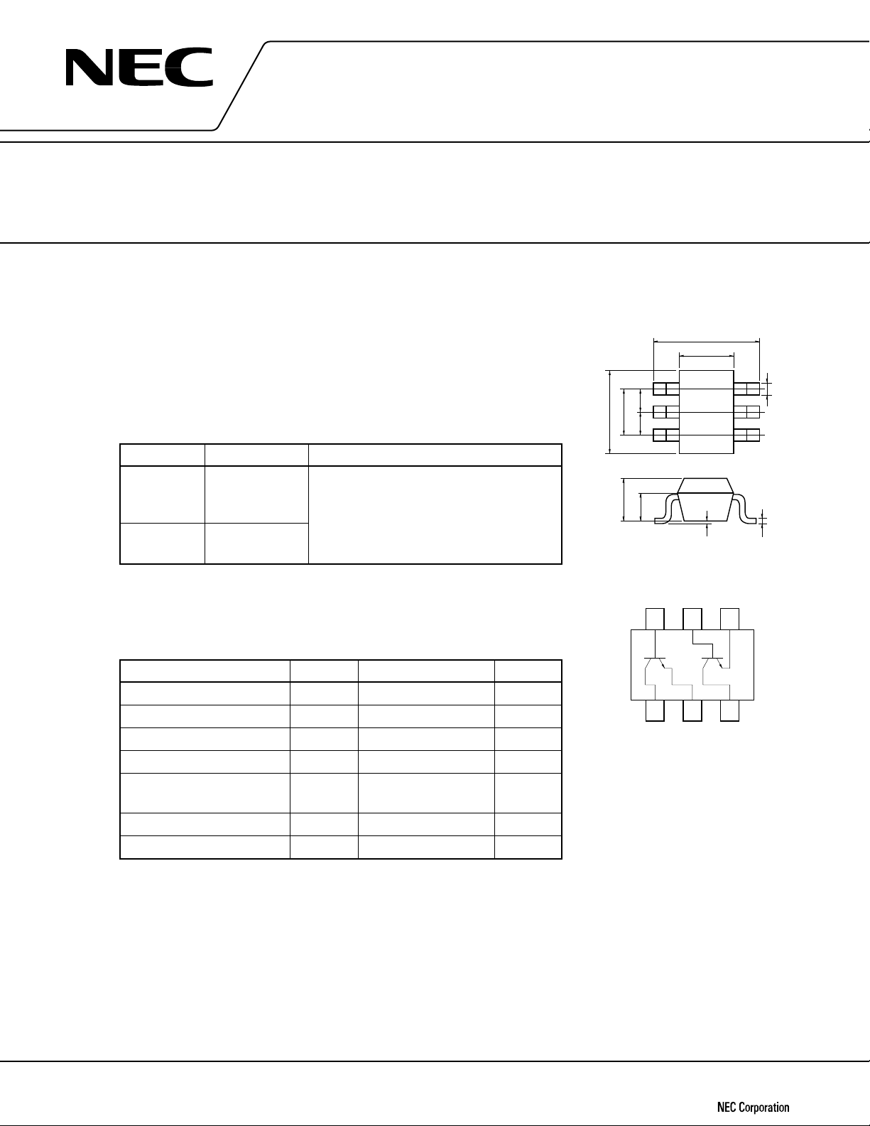
(WITH BUILT-IN 2 ELEMENTS) MINI MOLD
FEATURES PACKAGE DRAWINGS
• Low Noise, High Gain (Unit: mm)
• Operable at Low Voltage
• Small Feed-back Capacitance
re = 0.4 pF TYP.
C
• Built-in 2 Transistors (2 × 2SC4959)
ORDERING INFORMATION
1.3
2.0±0.2
0.650.65
2.1±0.1
1.25±0.1
123
XY
654
–0
+0.1
0.2
PART NUMBER
µ
PA806T Loose products Embossed tape 8 mm wide. Pin 6 (Q1
µ
PA806T-T1 Taping products
Remark If you require an evaluation sample, please contact an NEC
QUANTITY PACKING STYLE
(50 PCS) Base), Pin 5 (Q2 Base), Pin 4 (Q2 Emitter)
face to perforation side of the tape.
(3 KPCS/Reel)
PIN CONFIGURATION (Top View)
Sales Representative. (Unit sample quantity is 50 pcs.)
ABSOLUTE MAXIMUM RATINGS (TA = 25 °C)
PARAMETER SYMBOL RATING UNIT
Collector to Base Voltage VCBO 9V
Collector to Emitter Voltage VCEO 6V
Emitter to Base Voltage VEBO 2V
Collector Current IC 30 mA
Total Power Dissipation PT 150 in 1 element mW
200 in 2 elements
Junction Temperature Tj 150 ˚C
Storage Temperature Tstg –65 to +150 ˚C
Note
0.7
0.9±0.1
654
1
Q
123
PIN CONNECTIONS
1. Collector (Q1)
2. Emitter (Q1)
3. Collector (Q2)
0~0.1
Q
2
4. Emitter (Q2)
5. Base (Q2)
6. Base (Q1)
+0.1
–0
0.15
Note 110 mW must not be exceeded in 1 element.
Document No. ID-3640
(O.D. No. ID-9147)
Date Published April 1995 P
Printed in Japan
The information in this document is subject to change without notice.
©
1995
ELECTRICAL CHARACTERISTICS (TA = 25 °C)
PARAMETER SYMBOL CONDITION MIN. TYP. MAX. UNIT
Collector Cutoff Current ICBO VCB = 5 V, IE = 0 0.1
Emitter Cutoff Current IEBO VEB = 1 V, IC = 0 0.1
DC Current Gain hFE VCE = 3 V, IC = 10 mA
Gain Bandwidth Product fT VCE = 3 V, IC = 10 mA, f = 2 GHz 12 GHz
Feed-back Capacitance Cre VCB = 3 V, IE = 0, f = 1 MHz
Insertion Power Gain |S21|
2
VCE = 3 V, IC = 10 mA, f = 2 GHz 7 8.5 dB
Noise Figure NF VCE = 3 V, IC = 3 mA, f = 2 GHz 1.5 2.5 dB
hFE Ratio hFE1/hFE2 VCE = 3 V, IC = 10 mA 0.85
A smaller value among
hFE of hFE1 = Q1, Q2
A larger value among
hFE of hFE2 = Q1, Q2
Notes 1. Pulse Measurement: Pw ≤ 350 µs, Duty cycle ≤ 2 %
2. Measured with 3-pin bridge, emitter and case should be connected to guard pin of bridge.
Note 1
Note 2
75 150
0.4 0.7 pF
µ
PA806T
µ
A
µ
A
hFE CLASSIFICATION
Rank KB
Marking T83
hFE Value 75 to 150
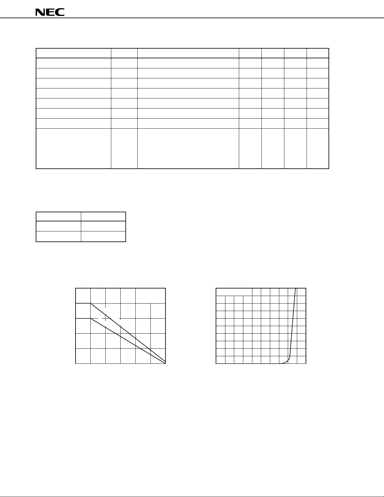
TYPICAL CHARACTERISTICS (TA = 25 °C)
TOTAL POWER DISSIPATION
vs. AMBIENT TEMPERATURE
Free Air
200
(mW)
T
100
Total Power Dissipation P
0
2 Elements in Total
Per Element
50 100 150
Ambient Temperature TA (°C)
COLLECTOR CURRENT vs.
BASE TO EMITTER VOLTAGE
50
VCE = 3 V
40
(mA)
C
30
20
Collector Current I
10
0
Base to Emitter Voltage VBE (V)
0.5 1.0
2

µ
PA806T
Collector Current IC (mA)
Gain Bandwidth Product fT (GHz)
COLLECTOR CURRENT vs.
COLLECTOR TO EMITTER VOLTAGE
60
50
40
30
20
10
0
Collector to Emitter Voltage VCE (V)
GAIN BANDWIDTH PRODUCT
vs. COLLECTOR CURRENT
14
f = 2 GHz
12
10
8
6
4
2
0.5
12 51020 50 1
Collector Current IC (mA)
500 µA
400 µA
300 µA
200 µA
IB = 100 µA
5 V
3 V
VCE = 1 V
DC Current Gain hFE
(dB)
2
Insertion Power Gain l S21e l
200
100
0
0.2 0.5 1 2
0.1
10
f = 2 GHz
8
6
4
2
DC CURRENT GAIN vs.
COLLECTOR CURRENT
5 V
VCE = 3 V
5 10 20 50 100
Collector Current IC (mA)
INSERTION GAIN vs.
COLLECTOR CURRENT
5 V
3 V
VCE = 1 V
2 5 10 20 50
Collector Current IC (mA)
4
3
2
Noise Figure NF (dB)
1
0
0.5
12 5 20 50
NOISE FIGURE vs.
COLLECTOR CURRENT
10
Collector Current I
C (mA)
f = 2 GHz
V
CE = 3 V
Feed-back Capacitance Cre (pF)
FEED-BACK CAPACITANCE vs.
COLLECTOR TO BASE VOLTAGE
0.6
0.5
0.4
0.3
0.2
0.5
2
1 5 10 20
Collector to Base Voltage VCB (V)
f = 1 MHz
3

S-PARAMETERS
VCE = 3 V, IC = 1 mA, ZO = 50 Ω
f S11 S21 S12 S22
GHz MAG ANG MAG ANG MAG ANG MAG ANG
0.200 0.9340 –15.7 3.5100 164.8 0.0450 82.6 0.9850 –8.7
0.400 0.9040 –29.4 3.3520 150.7 0.0780 68.0 0.9410 –17.1
0.600 0.8150 –43.4 3.1060 138.0 0.1140 62.8 0.8960 –23.6
0.800 0.7530 –56.6 2.8840 126.3 0.1370 58.0 0.8260 –29.9
1.000 0.6540 –68.9 2.6050 115.1 0.1490 55.2 0.7830 –34.7
1.200 0.5900 –79.8 2.4490 105.4 0.1660 45.4 0.7220 –38.0
1.400 0.5160 –90.1 2.2610 96.8 0.1770 44.8 0.6790 –42.0
1.600 0.4590 –101.5 2.0780 89.4 0.1780 45.1 0.6430 –45.2
1.800 0.4230 –110.8 1.9250 83.7 0.1880 42.5 0.6290 –46.8
2.000 0.3670 –123.9 1.8700 76.3 0.1900 41.9 0.5880 –51.4
2.200 0.3370 –136.7 1.7790 69.9 0.2110 43.9 0.5630 –54.3
2.400 0.3150 –145.5 1.6600 64.1 0.2140 41.9 0.5520 –57.0
2.600 0.3080 –159.1 1.5690 59.4 0.2070 42.8 0.5450 –59.2
2.800 0.2930 –164.8 1.5190 55.3 0.2140 45.8 0.5220 –64.5
3.000 0.2950 –179.6 1.4610 50.7 0.2260 45.4 0.4960 –61.3
VCE = 3 V, IC = 3 mA, ZO = 50 Ω
µ
PA806T
f S11 S21 S12 S22
GHz MAG ANG MAG ANG MAG ANG MAG ANG
0.200 0.8020 –25.9 8.8990 154.2 0.0370 67.2 0.9420 –15.7
0.400 0.6780 –45.8 7.4880 134.4 0.0760 65.6 0.8040 –26.6
0.600 0.5440 –62.8 6.1260 119.6 0.0860 60.9 0.7060 –33.2
0.800 0.4430 –75.7 5.1230 108.1 0.1050 58.4 0.6250 –36.6
1.000 0.3540 –87.3 4.3050 99.1 0.1210 55.9 0.5660 –38.3
1.200 0.2930 –99.7 3.7880 91.3 0.1330 61.2 0.5190 –41.4
1.400 0.2360 –108.4 3.3560 84.8 0.1440 55.4 0.4950 –43.9
1.600 0.2000 –121.0 3.0100 79.1 0.1570 56.2 0.4660 –44.5
1.800 0.1820 –129.5 2.6960 74.4 0.1760 58.0 0.4560 –44.5
2.000 0.1480 –151.7 2.5340 69.4 0.1940 56.1 0.4310 –48.8
2.200 0.1370 –166.1 2.3820 64.0 0.2150 56.3 0.4050 –51.9
2.400 0.1340 175.2 2.1870 60.0 0.2130 57.8 0.3990 –52.8
2.600 0.1640 169.7 2.0530 55.8 0.2410 57.6 0.3950 –52.9
2.800 0.1500 170.9 1.9660 53.0 0.2490 55.2 0.3750 –59.2
3.000 0.1780 147.7 1.8710 49.6 0.2750 56.6 0.3740 –60.8
4

S-PARAMETERS
VCE = 3 V, IC = 5 mA, ZO = 50 Ω
f S11 S21 S12 S22
GHz MAG ANG MAG ANG MAG ANG MAG ANG
0.200 0.6900 –33.3 12.2960 147.1 0.0320 74.8 0.8850 –19.7
0.400 0.5360 –54.7 9.4300 125.5 0.0610 66.3 0.7210 –30.3
0.600 0.4010 –70.0 7.2390 111.3 0.0700 59.6 0.6030 –34.5
0.800 0.3150 –82.4 5.8220 101.1 0.0950 63.8 0.5230 –36.7
1.000 0.2360 –93.8 4.7830 93.4 0.1090 62.3 0.4870 –38.0
1.200 0.1850 –105.4 4.1700 86.4 0.1260 61.9 0.4600 –38.8
1.400 0.1440 –115.8 3.6410 80.7 0.1350 65.9 0.4360 –40.4
1.600 0.1230 –134.4 3.2380 76.1 0.1560 61.2 0.4170 –42.6
1.800 0.1040 –144.6 2.8910 71.4 0.1770 62.4 0.4020 –43.9
2.000 0.1000 –170.6 2.7040 67.3 0.1930 60.7 0.3940 –45.8
2.200 0.1110 167.4 2.5330 62.6 0.2080 60.6 0.3710 –50.3
2.400 0.1040 158.2 2.3270 58.7 0.2260 61.6 0.3500 –50.2
2.600 0.1180 156.3 2.1850 54.9 0.2560 58.2 0.3560 –51.2
2.800 0.1190 150.0 2.0910 52.6 0.2560 56.8 0.3520 –58.1
3.000 0.1490 142.4 1.9760 49.0 0.2860 56.6 0.3410 –56.9
VCE = 3 V, IC = 10 mA, ZO = 50 Ω
µ
PA806T
f S11 S21 S12 S22
GHz MAG ANG MAG ANG MAG ANG MAG ANG
0.200 0.5080 –43.6 17.0900 135.9 0.0330 63.8 0.7930 –26.2
0.400 0.3410 –65.3 11.3980 114.2 0.0520 68.5 0.5910 –32.9
0.600 0.2320 –80.7 8.2250 102.0 0.0690 69.0 0.5130 –32.9
0.800 0.1770 –90.8 6.3950 93.8 0.0880 71.6 0.4480 –32.8
1.000 0.1220 –108.2 5.1870 87.2 0.1060 69.3 0.4180 –35.9
1.200 0.1010 –121.8 4.4390 81.6 0.1260 70.1 0.4030 –33.3
1.400 0.0670 –138.2 3.8770 76.9 0.1450 70.5 0.3930 –36.5
1.600 0.0620 –167.6 3.4350 72.4 0.1590 65.5 0.3680 –36.2
1.800 0.0660 –171.3 3.0650 68.8 0.1790 65.0 0.3610 –39.5
2.000 0.0770 146.7 2.8540 65.0 0.2060 63.9 0.3480 –42.3
2.200 0.0990 146.5 2.6590 60.5 0.2220 62.8 0.3360 –46.6
2.400 0.1140 128.1 2.4400 57.0 0.2420 60.9 0.3370 –48.8
2.600 0.1260 136.8 2.2790 53.5 0.2660 59.9 0.3170 –47.2
2.800 0.1020 129.6 2.1950 50.9 0.2770 59.6 0.3280 –55.1
3.000 0.1370 123.5 2.0800 47.9 0.2860 58.3 0.3100 –51.2
5

µ
PA806T
[MEMO]
No part of this document may be copied or reproduced in any form or by any means without the prior written
consent of NEC Corporation. NEC Corporation assumes no responsibility for any errors which may appear in this
document.
NEC Corporation does not assume any liability for infringement of patents, copyrights or other intellectual
property rights of third parties by or arising from use of a device described herein or any other liability arising
from use of such device. No license, either express, implied or otherwise, is granted under any patents,
copyrights or other intellectual property rights of NEC Corporation or others.
While NEC Corporation has been making continuous effort to enhance the reliability of its semiconductor devices,
the possibility of defects cannot be eliminated entirely. To minimize risks of damage or injury to persons or
property arising from a defect in an NEC semiconductor device, customer must incorporate sufficient safety
measures in its design, such as redundancy, fire-containment, and anti-failure features.
NEC devices are classified into the following three quality grades:
“Standard“, “Special“, and “Specific“. The Specific quality grade applies only to devices developed based on
a customer designated “quality assurance program“ for a specific application. The recommended applications
of a device depend on its quality grade, as indicated below. Customers must check the quality grade of each
device before using it in a particular application.
Standard: Computers, office equipment, communications equipment, test and measurement equipment,
audio and visual equipment, home electronic appliances, machine tools, personal electronic
equipment and industrial robots
Special: Transportation equipment (automobiles, trains, ships, etc.), traffic control systems, anti-disaster
systems, anti-crime systems, safety equipment and medical equipment (not specifically designed
for life support)
Specific: Aircrafts, aerospace equipment, submersible repeaters, nuclear reactor control systems, life
support systems or medical equipment for life support, etc.
The quality grade of NEC devices in “Standard“ unless otherwise specified in NEC's Data Sheets or Data Books.
If customers intend to use NEC devices for applications other than those specified for Standard quality grade,
they should contact NEC Sales Representative in advance.
Anti-radioactive design is not implemented in this product.
M4 94.11
6
 Loading...