

PRELIMINARY DATA SHEET
Silicon Transistor
µµµµ
PA833TF
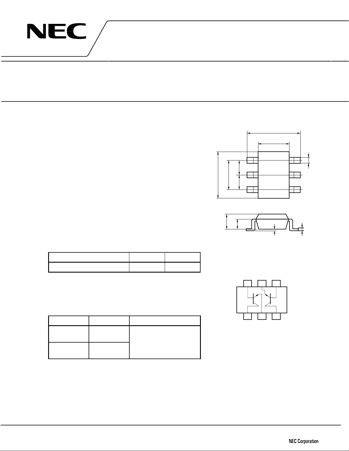
NPN SILICON EPITAXIAL TRANSISTOR (WITH 2 DIFFERENT ELEMENTS)
IN A 6-PIN THIN-TYPE SMALL MINI MOLD PACKAGE
DESCRIPTION PACKAGE DRAWINGS (Unit:mm)
The µPA833TF has two different built-in transistors (Q1
and Q2) for low noise amplification in the VHF band to UHF
band.
FEATURES
•Low noise
Q1 : NF = 1.7 dB TYP. @ f = 2 GHz, VCE = 1 V, IC = 3 mA
Q2 : NF = 1.5 dB TYP. @ f = 2 GHz, VCE = 3 V, IC = 3 mA
•High gain
Q1 : |S
Q2 : |S
•6-pin thin-type small mini mold package
•2 different transistors on-chip (2SC5193, 2SC4959)
2
21e
|
= 3.5 dB TYP. @ f = 2 GHz, VCE = 1 V, IC = 3 mA
2
21e
|
= 8.5 dB TYP. @ f = 2 GHz, VCE = 3 V, IC = 10 mA
ON-CHIP TRANSISTORS
1.30
2.00±0.2
0.60±0.1
0.65
0.65
0.45
2.10±0.1
1.25±0.1
V44
321
0 to 0.1
456
+0.1
−0.05
0.22
0.13±0.05
Q1 Q2
3-pin small mini mold part No. 2SC5193 2SC4959
The µPA836TF features the Q1 and Q2 in inverted positions.
ORDERING INFORMATION
PART NUMBER QUANTITY PACKING STYLE
µ
PA833TF
µ
PA833TF-T1
Caution is required concerning excess input, such as from static electricity, because the high-frequency
process is used for this device.
Loose products
(50 pcs)
Taping products
(3 kpcs/reel)
The information in this document is subject to change without notice.
8-mm wide embossed tape.
Pin 6 (Q1 Base), pin 5 (Q2
Emitter), and pin 4 (Q2 Base)
face perforated side of tape.
PIN CONFIGURATION (Top View)
B1
E2 B2
654
Q1 Q2
321
C1 E1 C2
PIN CONNECTIONS
1. Collector (Q1)
2. Emitter (Q1)
3. Collector (Q2)
4. Base (Q2)
5. Emitter (Q2)
6. Base (Q1)
Document No. P12725EJ1V0DS00 (1st edition)
Date Published August 1997 N
Printed in Japan
1997©
µµµµ
PA833TF
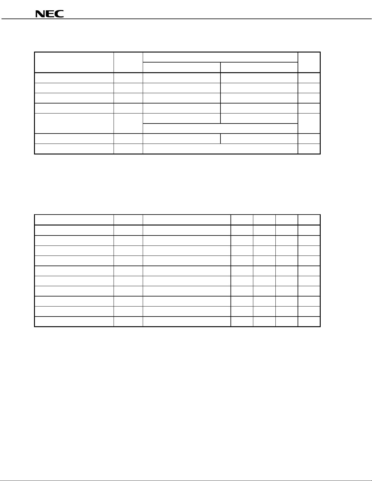
ABSOLUTE MAXIMUM RATINGS (TA = 25
Collector to base voltage V
Collector to emitter voltage V
Emitter to base voltage V
Collector current I
Total power dissipation P
Junction temperature T
Storage temperature T
Note
110 mW must not be exceeded for 1 element.
(1) Q1
CBO
CEO
EBO
C
T
j
stg
ELECTRICAL CHARACTERISTICS
°°°°
C)
RATING
Q1 Q2
99V
66V
22V
100 30 mA
150 in 1 element 150 in 1 element mW
200 in 2 elements
Note
150 150
−
65 to +150
UNITSYMBOLPARAMETER
°
C
°
C
PARAMETER SYMBOL CONDITION MIN. TYP. MAX. UNIT
Collector cutoff current I
Emitter cutoff current I
DC current gain h
Gain bandwidth product (1) f
Gain bandwidth product (2) f
Feedback capacitance C
Insertion power gain (1)
Insertion power gain (2)
CBO
EBO
FE
T
T
|
21e
S
|
21e
S
VCB = 5 V, IE = 0 0.1
VEB = 1 V, IC = 0 0.1
VCE = 1 V, IC = 3 mA
Note 1
100 145
VCE = 1 V, IC = 3 mA, f = 2 GHz 4.0 4.5 GHz
VCE = 3 V, IC = 20 mA, f = 2 GHz 9.0 GHz
VCB = 1 V, IE = 0, f = 1 MHz
re
2
|
VCE = 1 V, IC = 3 mA, f = 2 GHz 2.5 3.5 dB
2
|
VCE = 3 V, IC = 20 mA, f = 2 GHz 6.5 dB
Note 2
0.75 0.85 pF
Noise figure (1) NF VCE = 1 V, IC = 3 mA, f = 2 GHz 1.7 2.5 dB
Noise figure (2) NF VCE = 3 V, IC = 7 mA, f = 2 GHz 1.5 dB
Notes 1.
Pulse measurement: PW ≤ 350
Collector to base capacitance when measured with capacitance meter (automatic balanced bridge
2.
s, Duty cycle ≤ 2%
µ
method), with emitter connected to guard pin of capacitance meter.
µ
A
µ
A
2

µµµµ
PA833TF
(2) Q2
ELECTRICAL CHARACTERISTICS
PARAMETER SYMBOL CONDITION MIN. TYP. MAX. UNIT
Collector cutoff current I
Emitter cutoff current I
DC current gain h
Gain bandwidth product f
Feedback capacitance C
Insertion power gain
Noise figure NF VCE = 3 V, IC = 3 mA, f = 2 GHz 1.5 2.5 dB
CBO
EBO
FE
T
|
21e
S
VCB = 5 V, IE = 0 0.1
VEB = 1 V, IC = 0 0.1
VCE = 3 V, IC = 10 mA
Note 1
75 150
VCE = 3 V, IC = 10 mA, f = 2 GHz 12 GHz
VCB = 3 V, IE = 0, f = 1 MHz
re
2
|
VCE = 3 V, IC = 10 mA, f = 2 GHz 7 8.5 dB
Note 2
0.4 0.7 pF
µ
A
µ
A
Notes 1.
Pulse measurement: PW ≤ 350
Collector to base capacitance when measured with capacitance meter (automatic balanced bridge
2.
method), with emitter connected to guard pin of capacitance meter.
hFE CLASSIFICATION
Rank FB
Marking V44
hFE value of Q1 100 to 145
hFE value of Q2 75 to 150
s, Duty cycle ≤ 2%
µ
3
µµµµ
PA833TF
TYPICAL CHARACTERISTICS (TA = 25
Q1 Q2
Total Power Dissipation vs. Ambient Temperature
200
(mW)
T
2 elements in total
100
Total power dissipation P
0
50 100 150
Ambient temperature TA (˚C)
Collector Current vs. DC Base Voltage
100
V
CE
50
= 1 V
20
10
(mA)
5
C
2
1
0.5
0.2
0.1
Collector current I
0.05
0.02
0.01
0 0.5 1
DC base voltage V
Free Air
Q1 when using
1 element
Q1 when using
2 elements
BE
(V)
°°°°
C)
Total Power Dissipation vs. Ambient Temperature
Free Air
Q2 when using
200
(mW)
T
2 elements in total
1 element
Q2 when using
100
2 elements
Total power dissipation P
0 50 100 150
A
Ambient temperature T
(˚C)
Collector Current vs. DC Base Voltage
50
V
CE
= 3 V
40
(mA)
C
30
20
Collector current I
10
0
DC base voltage V
0.5 1.0
BE
(V)
Collector Current vs. Collector to Emitter Voltage
30
200 A
180 A
(mA)
C
20
160 A
140 A
120 A
100 A
10
Collector current I
IB = 20 A
0 123456
Collector to emitter voltage V
CE
4
µ
µ
µ
µ
µ
µ
µ
80 A
µ
60 A
µ
40 A
(V)
Collector Current vs. Collector to Emitter Voltage
60
500 A
µ
50
(mA)
C
40
30
400 A
µ
300 A
µ
µ
200 A
20
µ
B
= 100 A
Collector current I
10
I
µ
0 246
135
Collector to emitter voltage V
CE
(V)
Q1 Q2
µµµµ
PA833TF
DC Current Gain vs. Collector Current
200
VCE = 1 V
FE
100
DC current gain h
0
0.1 0.2 10.5 10 20 5025
Collector current IC (mA)
Gain Bandwidth Product vs. Collector Current
10
f = 2 GH
)
Z
(GH
T
Z
VCE = 1 V
5
100
DC Current Gain vs. Collector Current
200
FE
5 V
VCE = 3 V
100
DC current gain h
0
0.2 2
0.1
0.5 1 5 10 50 100
20
Collector current IC (mA)
Gain Bandwidth Product vs. Collector Current
14
)
Z
(GH
T
f = 2 GHz
12
10
8
5 V
3 V
VCE = 1 V
Gain bandwidth product f
0
1235710
Collector current IC (mA)
Insertion Power Gain vs. Collector Current
10
f = 2 GH
Z
VCE = 1 V
(dB)
2
21e
5
Insertion power gain S
0
1235710
Collector current IC (mA)
6
4
Gain bandwidth product f
2
0.5
12 510
Collector current IC (mA)
Insertion Power Gain vs. Collector Current
10
f = 2 GHz
(dB)
2
8
21e
6
4
Insertion power gain S
2
0.5
2
510
Collector current IC (mA)
20
VCE = 1 V
20
50
5 V
3 V
50
5

Q1 Q2
Noise Figure vs. Collector Current
3
f = 2 GH
Z
VCE = 1 V
Noise Figure vs. Collector Current
4
3
µµµµ
PA833TF
f = 2 GHz
V
CE
= 3 V
2
Noise figure NF (dB)
f = 1 GH
Z
1
1235
Collector current IC (mA)
Feedback Capacitance vs. Collector to Base Voltage
f = 1 MH
(pF)
re
1.0
0.5
Feedback capacitance C
0.1
1
Collector to base voltage V
510
CB
(V)
710
Z
20
2
1
Noise figure NF (dB)
0
0.55012 510
20
Collector current IC (mA)
Feedback Capacitance vs. Collector to Base Voltage
0.6
f = 1 MHz
(pF)
0.5
re
0.4
0.3
Feedback capacitance C
0.2
0.5
12 510
CB
Collector to base voltage V
(V)
20
Maximum Available Gain, Insertion Power Gain vs. Frequency
VCE = 1 V
C
= 5 mA
I
30
21e
MAG
2
(dB)
2
21e
20
S
10
0
Maximum available power gain MAG (dB)
Insertion power gain S
0.1 0.5 1 5
Frequency f (GHZ)
6
Maximum Available Gain, Insertion Power Gain vs. Frequency
25
V
CE
= 3 V
C
= 10 mA
I
20
(dB)
2
21e
15
10
MAG
S
21e
2
5
Maximum available power gain MAG (dB)
Insertion power gain S
0
0.1
0.2 0.5 1 2 5
Z
Frequency f (GH
)

Q1
Noise Figure vs. Frequency
VCE = 1 V
1.5
1
Noise figure NF (dB)
0.5
0.1 0.5 1.0 2
Frequency f (GHz)
I
C
= 5 mA
µµµµ
PA833TF
7

S-PARAMETERS Q1
VCE = 3 V, IC = 1 mA, Z0 = 50
FREQUENCY S11 S21 S12 S22
GHz MAG ANG MAG ANG MAG ANG MAG ANG
.10
.20
.30
.40
.50
.60
.70
.80
.90
1.00
1.10
1.20
1.30
1.40
1.50
1.60
1.70
1.80
1.90
2.00
2.10
2.20
2.30
2.40
2.50
2.60
2.70
2.80
2.90
3.00
.97
.95
.91
.87
.83
.79
.75
.71
.68
.66
.64
.62
.61
.61
.61
.61
.61
.62
.63
.63
.64
.65
.66
.67
.67
.68
.69
.70
.71
.72
Ω
−
14.33
−
28.67
−
42.88
−
56.75
−
70.72
−
84.33
−
97.41
−
109.76
−
122.09
−
133.22
−
144.02
−
154.11
−
163.41
−
172.15
179.69
172.31
165.55
159.12
153.12
147.73
142.54
137.65
133.23
129.32
125.32
121.78
118.50
115.24
112.33
109.50
2.43
2.38
2.36
2.27
2.23
2.16
2.08
1.99
1.92
1.82
1.74
1.66
1.57
1.50
1.43
1.36
1.29
1.24
1.18
1.12
1.08
1.03
.99
.95
.92
.88
.85
.82
.79
.76
166.54
154.71
144.04
134.07
125.01
116.71
108.43
101.04
93.80
87.30
81.47
75.63
70.50
65.55
60.93
56.58
52.57
48.65
44.96
41.71
38.29
35.21
32.01
29.64
27.04
24.60
22.41
20.14
18.25
16.28
.04
.07
.10
.13
.15
.16
.17
.17
.18
.18
.18
.18
.17
.17
.17
.16
.16
.15
.15
.15
.15
.15
.15
.15
.15
.16
.17
.17
.18
.19
80.24
70.60
62.11
54.03
47.25
40.79
35.62
31.08
26.89
23.81
21.08
19.11
17.32
16.33
15.48
15.52
15.97
16.87
18.29
20.29
22.73
25.25
27.87
30.83
33.50
36.03
38.41
40.23
41.83
42.71
.99
.97
.92
.88
.83
.78
.75
.70
.67
.64
.62
.60
.58
.57
.56
.54
.54
.53
.52
.52
.51
.51
.51
.50
.50
.50
.50
.50
.50
.50
µµµµ
PA833TF
−
7.18
−
13.99
−
19.89
−
25.53
−
29.96
−
34.25
−
37.36
−
40.60
−
43.12
−
45.41
−
47.82
−
49.75
−
51.90
−
54.11
−
56.32
−
58.59
−
61.07
−
63.68
−
66.32
−
69.09
−
71.98
−
75.26
−
78.60
−
82.11
−
85.80
−
89.61
−
93.50
−
97.66
−
101.66
−
105.83
VCE = 3 V, IC = 3 mA, Z0 = 50
FREQUENCY S11 S21 S12 S22
GHz MAG ANG MAG ANG MAG ANG MAG ANG
.10
.20
.30
.40
.50
.60
.70
.80
.90
1.00
1.10
1.20
1.30
1.40
1.50
1.60
1.70
1.80
1.90
2.00
2.10
2.20
2.30
2.40
2.50
2.60
2.70
2.80
2.90
3.00
.91
.84
.77
.69
.62
.57
.52
.49
.47
.46
.46
.46
.46
.47
.47
.48
.49
.50
.51
.52
.53
.54
.55
.57
.58
.59
.60
.61
.62
.63
Ω
−
20.87
−
40.75
−
60.61
−
79.21
−
96.87
−
112.43
−
126.51
−
139.31
−
150.57
−
160.97
−
170.30
−
178.72
173.69
166.63
160.24
154.42
149.16
144.23
139.58
135.44
131.39
127.65
124.36
121.18
118.19
115.58
112.99
110.43
108.13
105.91
6.85
6.38
6.07
5.65
5.20
4.72
4.31
3.94
3.59
3.31
3.05
2.83
2.64
2.47
2.32
2.19
2.07
1.96
1.86
1.77
1.70
1.62
1.55
1.49
1.43
1.38
1.33
1.29
1.24
1.20
160.51
145.81
133.27
122.38
112.63
104.66
97.30
91.09
85.51
80.44
75.95
71.60
67.73
63.86
60.26
56.86
53.60
50.43
47.34
44.29
41.48
38.94
36.05
33.64
31.34
28.95
26.70
24.45
22.28
20.22
.04
.06
.08
.10
.11
.12
.12
.13
.13
.14
.14
.14
.15
.15
.16
.16
.17
.17
.18
.18
.19
.20
.20
.21
.22
.22
.23
.24
.24
.25
76.06
64.42
55.69
49.28
45.15
41.99
40.07
38.98
38.14
38.00
37.60
37.86
37.91
38.15
38.28
38.60
38.76
39.12
38.98
39.31
39.23
39.28
39.08
39.04
39.03
38.56
38.53
38.23
37.87
37.38
.95
.87
.77
.68
.61
.54
.50
.46
.42
.40
.38
.36
.34
.33
.32
.31
.30
.29
.28
.28
.27
.26
.26
.26
.26
.26
.26
.26
.26
.26
−
14.18
−
26.10
−
34.95
−
41.90
−
46.55
−
50.59
−
53.40
−
55.90
−
58.00
−
60.02
−
62.10
−
63.86
−
66.00
−
68.28
−
70.83
−
73.24
−
76.06
−
78.94
−
81.98
−
85.18
−
88.50
−
92.55
−
96.16
−
100.32
−
104.63
−
109.15
−
113.50
−
118.22
−
122.53
−
126.83
8

S-PARAMETERS Q1
VCE = 3 V, IC = 5 mA, Z0 = 50
FREQUENCY S11 S21 S12 S22
GHz MAG ANG MAG ANG MAG ANG MAG ANG
.10
.20
.30
.40
.50
.60
.70
.80
.90
1.00
1.10
1.20
1.30
1.40
1.50
1.60
1.70
1.80
1.90
2.00
2.10
2.20
2.30
2.40
2.50
2.60
2.70
2.80
2.90
3.00
.85
.75
.64
.56
.49
.45
.42
.41
.40
.40
.40
.41
.41
.42
.43
.44
.45
.46
.48
.49
.50
.51
.52
.53
.54
.56
.57
.58
.59
.60
Ω
−
26.44
−
51.20
−
75.20
−
96.72
−
115.03
−
130.31
−
143.59
−
155.39
−
165.50
−
174.72
177.10
169.76
163.14
157.10
151.58
146.60
142.01
137.81
133.84
130.04
126.68
123.26
120.32
117.64
114.93
112.60
110.25
108.05
105.95
103.96
10.69
9.61
8.75
7.76
6.80
5.95
5.26
4.72
4.25
3.87
3.55
3.28
3.04
2.83
2.66
2.50
2.36
2.23
2.12
2.01
1.93
1.83
1.76
1.69
1.62
1.56
1.50
1.46
1.41
1.36
155.98
139.24
125.25
113.92
104.72
97.69
91.52
86.26
81.56
77.29
73.37
69.66
66.19
62.87
59.70
56.66
53.73
50.83
48.10
45.17
42.52
40.17
37.50
35.27
32.99
30.62
28.52
26.39
24.29
22.18
.03
.06
.07
.08
.09
.10
.11
.11
.12
.13
.13
.14
.15
.16
.16
.17
.18
.19
.19
.20
.21
.22
.22
.23
.24
.25
.25
.26
.27
.27
73.46
61.17
54.17
50.16
48.17
47.13
46.84
46.85
46.62
46.83
46.91
46.94
46.69
46.57
46.31
45.94
45.59
45.07
44.55
44.01
43.30
42.61
41.82
41.27
40.36
39.55
38.85
38.08
37.27
36.49
µµµµ
PA833TF
.92
.79
.65
.55
.48
.42
.38
.35
.32
.30
.28
.27
.25
.24
.23
.22
.22
.21
.21
.20
.20
.20
.19
.20
.20
.20
.20
.21
.21
.21
−
19.86
−
34.91
−
44.33
−
51.20
−
55.56
−
59.25
−
61.89
−
64.36
−
66.67
−
68.91
−
71.34
−
73.69
−
76.39
−
79.41
−
82.66
−
86.03
−
89.61
−
93.69
−
97.41
−
101.67
−
105.84
−
111.09
−
115.75
−
120.90
−
125.90
−
131.14
−
136.28
−
141.19
−
145.61
−
149.97
VCE = 3 V, IC = 7 mA, Z0 = 50
FREQUENCY S11 S21 S12 S22
GHz MAG ANG MAG ANG MAG ANG MAG ANG
.10
.20
.30
.40
.50
.60
.70
.80
.90
1.00
1.10
1.20
1.30
1.40
1.50
1.60
1.70
1.80
1.90
2.00
2.10
2.20
2.30
2.40
2.50
2.60
2.70
2.80
2.90
3.00
.79
.67
.55
.47
.42
.39
.38
.37
.37
.37
.38
.38
.39
.40
.41
.42
.44
.45
.46
.47
.48
.49
.50
.52
.53
.54
.55
.56
.58
.59
Ω
−
31.67
−
60.82
−
87.90
−
110.16
−
127.95
−
142.37
−
154.76
−
165.47
−
174.83
176.89
169.63
162.95
156.98
151.53
146.63
141.98
137.93
133.89
130.36
126.94
123.80
120.71
118.00
115.48
113.00
110.80
108.67
106.60
104.57
102.82
14.14
12.28
10.67
9.04
7.66
6.59
5.76
5.12
4.59
4.16
3.81
3.50
3.25
3.03
2.83
2.66
2.51
2.38
2.26
2.14
2.05
1.95
1.87
1.80
1.73
1.66
1.60
1.55
1.50
1.45
152.27
133.87
119.07
108.13
99.95
93.83
88.35
83.75
79.53
75.64
72.18
68.56
65.42
62.34
59.33
56.50
53.72
50.97
48.32
45.65
43.03
40.91
38.45
36.15
33.97
31.82
29.74
27.34
25.66
23.37
.03
.05
.06
.07
.08
.09
.10
.11
.12
.13
.13
.14
.15
.16
.17
.18
.19
.20
.20
.21
.22
.23
.24
.24
.25
.26
.26
.27
.28
.29
71.15
59.89
54.65
52.59
51.97
51.63
52.13
52.11
52.18
52.20
51.99
51.72
51.33
50.81
50.15
49.40
48.77
48.00
47.04
46.10
45.20
44.15
43.05
42.04
41.08
39.96
39.23
38.14
37.25
36.23
.88
.72
.57
.47
.40
.35
.32
.29
.27
.25
.23
.22
.21
.20
.19
.19
.18
.18
.18
.17
.17
.17
.18
.18
.18
.19
.19
.20
.21
.21
−
24.58
−
41.34
−
50.83
−
57.33
−
61.50
−
65.05
−
67.82
−
70.62
−
73.11
−
75.82
−
78.72
−
81.78
−
85.11
−
88.95
−
92.87
−
97.18
−
101.69
−
106.30
−
110.96
−
116.39
−
120.97
−
126.84
−
132.13
−
137.40
−
142.69
−
148.07
−
152.96
−
157.19
−
161.69
−
165.54
9

S-PARAMETERS Q1
VCE = 3 V, IC = 10 mA, Z0 = 50
FREQUENCY S11 S21 S12 S22
GHz MAG ANG MAG ANG MAG ANG MAG ANG
.10
.20
.30
.40
.50
.60
.70
.80
.90
1.00
1.10
1.20
1.30
1.40
1.50
1.60
1.70
1.80
1.90
2.00
2.10
2.20
2.30
2.40
2.50
2.60
2.70
2.80
2.90
3.00
.71
.57
.45
.39
.36
.35
.34
.34
.34
.35
.36
.37
.38
.39
.40
.41
.42
.43
.45
.46
.47
.48
.49
.50
.52
.53
.54
.55
.57
.58
Ω
−
39.03
−
73.63
−
102.58
−
124.33
−
141.02
−
154.37
−
165.44
−
175.03
176.63
169.25
162.75
156.83
151.50
146.60
142.12
138.03
134.21
130.67
127.37
124.22
121.31
118.37
115.87
113.55
111.30
109.28
107.16
105.27
103.43
101.61
18.58
15.31
12.43
10.08
8.36
7.10
6.16
5.44
4.87
4.40
4.02
3.70
3.42
3.19
2.98
2.80
2.63
2.50
2.37
2.25
2.15
2.05
1.96
1.89
1.81
1.74
1.67
1.62
1.57
1.51
147.71
127.39
112.73
102.91
95.89
90.47
85.73
81.62
77.75
74.22
71.00
67.77
64.82
61.79
59.04
56.45
53.75
51.05
48.74
46.04
43.60
41.36
38.90
36.95
34.71
32.62
30.43
28.76
26.44
24.93
.03
.05
.06
.07
.08
.09
.10
.11
.12
.13
.14
.15
.16
.17
.17
.18
.19
.20
.21
.22
.23
.24
.25
.25
.26
.27
.28
.28
.29
.30
68.69
59.38
56.68
56.27
56.57
56.86
57.18
57.18
57.09
56.69
56.34
55.55
54.83
53.99
53.03
52.03
51.04
49.91
48.75
47.77
46.48
45.20
43.97
42.65
41.70
40.45
39.28
38.16
37.04
36.10
.83
.63
.49
.40
.34
.29
.26
.24
.22
.21
.20
.19
.18
.17
.17
.16
.16
.16
.16
.16
.16
.17
.17
.18
.19
.19
.20
.21
.22
.23
µµµµ
PA833TF
−
30.16
−
48.07
−
57.41
−
63.51
−
67.57
−
71.19
−
74.31
−
77.41
−
80.56
−
83.81
−
87.55
−
91.34
−
95.70
−
100.40
−
104.99
−
110.36
−
115.48
−
120.86
−
126.15
−
131.74
−
136.39
−
142.70
−
147.46
−
152.75
−
157.66
−
162.35
−
166.91
−
170.83
−
174.49
−
177.86
VCE = 3 V, IC = 20 mA, Z0 = 50
FREQUENCY S11 S21 S12 S22
GHz MAG ANG MAG ANG MAG ANG MAG ANG
.10
.20
.30
.40
.50
.60
.70
.80
.90
1.00
1.10
1.20
1.30
1.40
1.50
1.60
1.70
1.80
1.90
2.00
2.10
2.20
2.30
2.40
2.50
2.60
2.70
2.80
2.90
3.00
.52
.39
.33
.31
.30
.30
.31
.31
.32
.33
.34
.35
.36
.37
.38
.40
.41
.42
.43
.44
.46
.47
.48
.49
.50
.51
.53
.54
.55
.56
Ω
−
60.10
−
103.44
−
130.53
−
148.95
−
162.62
−
172.99
178.35
170.80
164.26
158.34
153.02
148.21
143.86
139.65
135.96
132.38
129.06
126.14
123.11
120.40
117.80
115.23
112.96
110.86
108.77
106.98
105.14
103.40
101.60
100.10
28.62
19.94
14.51
11.26
9.15
7.69
6.63
5.84
5.21
4.70
4.28
3.94
3.63
3.38
3.16
2.97
2.79
2.64
2.50
2.38
2.27
2.16
2.07
1.99
1.90
1.84
1.77
1.72
1.65
1.61
137.10
115.16
103.51
96.02
90.56
86.27
82.36
78.82
75.55
72.35
69.45
66.66
63.96
61.26
58.61
56.19
53.72
51.32
48.96
46.54
44.17
42.21
39.64
37.96
35.67
33.82
31.79
29.93
28.01
26.09
.02
.04
.05
.06
.07
.08
.09
.11
.12
.13
.14
.15
.16
.17
.18
.19
.20
.21
.22
.23
.24
.25
.26
.27
.27
.28
.29
.30
.30
.31
67.35
63.08
63.34
64.33
65.01
65.06
64.97
64.40
63.46
62.64
61.47
60.45
59.09
58.05
56.50
55.17
53.77
52.54
51.02
49.64
48.25
46.65
45.13
43.59
42.37
40.93
39.70
38.37
37.05
35.76
.71
.48
.35
.28
.24
.21
.19
.18
.16
.16
.15
.15
.15
.15
.15
.15
.15
.16
.16
.17
.18
.18
.19
.20
.21
.22
.23
.24
.25
.26
−
41.30
−
59.79
−
68.39
−
74.25
−
78.55
−
82.95
−
87.11
−
91.38
−
96.07
−
100.35
−
105.51
−
110.63
−
116.00
−
121.72
−
127.25
−
133.07
−
138.41
−
143.83
−
148.58
−
153.87
−
157.74
−
162.91
−
167.09
−
171.04
−
174.96
−
178.81
177.40
174.62
171.56
168.73
10

S-PARAMETERS Q2
VCE = 3 V, IC = 1 mA, Z0 = 50
FREQUENCY S11 S21 S12 S22
GHz MAG ANG MAG ANG MAG ANG MAG ANG
.10
.20
.30
.40
.50
.60
.70
.80
.90
1.00
1.10
1.20
1.30
1.40
1.50
1.60
1.70
1.80
1.90
2.00
2.10
2.20
2.30
2.40
2.50
2.60
2.70
2.80
2.90
3.00
.98
.97
.95
.93
.90
.87
.84
.81
.77
.73
.69
.65
.62
.58
.54
.51
.47
.45
.42
.40
.38
.36
.35
.34
.33
.32
.32
.32
.32
.33
Ω
−
−
11.82
−
17.85
−
23.59
−
29.61
−
35.62
−
41.49
−
47.40
−
53.49
−
59.00
−
65.20
−
71.05
−
77.22
−
83.22
−
89.53
−
95.27
−
101.29
−
107.59
−
114.02
−
120.45
−
127.04
−
133.41
−
139.83
−
146.46
−
153.17
−
159.96
−
166.01
−
172.06
−
177.98
177.01
5.93
2.43
2.41
2.42
2.39
2.38
2.37
2.34
2.32
2.32
2.26
2.25
2.21
2.17
2.15
2.13
2.07
2.02
1.99
1.95
1.90
1.87
1.83
1.78
1.74
1.71
1.68
1.64
1.61
1.58
1.54
171.79
164.40
157.59
151.04
144.91
139.49
133.87
128.66
123.12
118.06
113.30
108.31
103.81
99.18
94.49
90.14
86.01
82.00
78.38
74.87
70.82
67.34
63.84
60.75
57.60
54.38
51.35
48.28
45.54
42.57
.02
.04
.05
.07
.09
.10
.11
.12
.13
.14
.15
.16
.16
.17
.17
.18
.18
.18
.19
.19
.19
.20
.20
.20
.21
.21
.22
.22
.23
.23
85.64
80.86
76.45
72.26
68.73
64.78
61.52
58.06
55.30
52.86
50.42
48.61
46.62
45.21
43.82
42.57
41.68
40.66
40.08
39.57
39.19
38.84
38.49
38.49
38.43
38.28
38.20
38.44
38.28
38.11
µµµµ
PA833TF
.99
.99
.97
.95
.93
.90
.87
.85
.82
.78
.76
.73
.70
.68
.66
.63
.61
.59
.57
.55
.53
.51
.50
.48
.46
.45
.43
.41
.40
.38
−
−
−
11.10
−
14.56
−
17.91
−
21.19
−
23.71
−
26.91
−
29.05
−
31.52
−
33.73
−
35.51
−
37.59
−
39.34
−
41.12
−
42.89
−
44.56
−
46.38
−
47.99
−
49.87
−
51.49
−
53.44
−
55.39
−
57.67
−
59.91
−
62.31
−
64.97
−
67.87
−
70.94
−
74.21
3.75
7.53
VCE = 3 V, IC = 3 mA, Z0 = 50
FREQUENCY S11 S21 S12 S22
GHz MAG ANG MAG ANG MAG ANG MAG ANG
.10
.20
.30
.40
.50
.60
.70
.80
.90
1.00
1.10
1.20
1.30
1.40
1.50
1.60
1.70
1.80
1.90
2.00
2.10
2.20
2.30
2.40
2.50
2.60
2.70
2.80
2.90
3.00
.93
.90
.84
.79
.72
.66
.59
.53
.48
.43
.38
.34
.31
.28
.26
.24
.22
.21
.20
.19
.18
.18
.18
.18
.19
.20
.20
.21
.22
.24
Ω
−
−
18.39
−
27.39
−
35.83
−
44.06
−
51.67
−
58.86
−
65.57
−
71.57
−
77.20
−
82.70
−
87.82
−
93.49
−
98.65
−
104.50
−
110.31
−
116.75
−
123.46
−
130.51
−
137.84
−
145.47
−
152.73
−
160.13
−
167.47
−
174.18
179.79
173.96
168.73
163.65
159.82
9.39
6.76
6.46
6.32
6.06
5.82
5.54
5.28
5.01
4.72
4.45
4.20
3.95
3.74
3.55
3.37
3.21
3.06
2.94
2.81
2.71
2.61
2.52
2.44
2.36
2.29
2.23
2.16
2.10
2.05
1.99
166.53
155.80
146.52
138.21
130.60
123.94
117.07
111.07
105.46
100.46
95.95
91.74
87.96
84.35
80.85
77.72
74.57
71.63
68.84
66.02
63.33
60.80
58.00
55.57
53.07
50.72
48.10
45.81
43.41
41.14
.02
.03
.05
.06
.07
.08
.09
.10
.10
.11
.12
.13
.13
.14
.15
.15
.16
.17
.18
.18
.19
.20
.21
.22
.22
.23
.24
.25
.26
.26
82.60
76.86
71.65
67.47
64.58
61.95
60.46
59.12
57.98
57.39
56.96
56.54
56.14
55.72
55.21
54.91
54.46
53.91
53.57
53.01
52.38
51.91
51.17
50.80
49.89
49.17
48.35
47.49
46.43
45.56
.98
.94
.89
.83
.77
.72
.68
.64
.60
.57
.55
.52
.50
.48
.46
.44
.43
.41
.39
.38
.36
.35
.33
.32
.30
.28
.27
.25
.24
.22
−
−
13.64
−
18.91
−
23.49
−
26.46
−
29.65
−
31.43
−
33.17
−
34.36
−
35.31
−
36.47
−
37.08
−
37.96
−
38.83
−
39.70
−
40.63
−
41.65
−
42.70
−
43.76
−
44.95
−
46.23
−
47.64
−
49.19
−
50.82
−
52.82
−
54.67
−
56.94
−
59.46
−
62.59
−
65.40
7.24
11

S-PARAMETERS Q2
VCE = 3 V, IC = 5 mA, Z0 = 50
FREQUENCY S11 S21 S12 S22
GHz MAG ANG MAG ANG MAG ANG MAG ANG
.10
.20
.30
.40
.50
.60
.70
.80
.90
1.00
1.10
1.20
1.30
1.40
1.50
1.60
1.70
1.80
1.90
2.00
2.10
2.20
2.30
2.40
2.50
2.60
2.70
2.80
2.90
3.00
.89
.83
.75
.66
.57
.50
.43
.37
.33
.29
.26
.23
.21
.19
.17
.16
.15
.14
.13
.13
.13
.13
.14
.15
.15
.17
.18
.19
.20
.22
Ω
−
12.31
−
23.63
−
34.70
−
44.55
−
53.23
−
60.42
−
66.51
−
71.94
−
76.60
−
81.19
−
85.79
−
90.41
−
95.79
−
100.84
−
106.89
−
113.52
−
120.69
−
128.54
−
136.73
−
145.48
−
153.95
−
161.96
−
169.65
−
177.12
176.33
170.73
165.64
160.85
156.69
153.43
10.46
9.75
9.25
8.62
7.96
7.27
6.64
6.08
5.57
5.15
4.77
4.45
4.17
3.91
3.70
3.50
3.33
3.18
3.04
2.92
2.81
2.71
2.61
2.53
2.45
2.37
2.31
2.24
2.18
2.12
162.72
149.86
138.82
129.30
120.72
113.73
107.23
101.84
97.19
92.96
89.24
85.71
82.52
79.44
76.63
73.79
71.22
68.57
66.08
63.46
61.14
58.79
56.38
53.98
51.77
49.49
47.17
45.04
42.82
40.65
.02
.03
.04
.06
.06
.07
.08
.09
.10
.10
.11
.12
.13
.14
.14
.15
.16
.17
.18
.19
.20
.20
.21
.22
.23
.24
.25
.26
.27
.27
81.62
74.55
69.69
66.77
64.98
63.78
63.28
62.73
62.37
62.23
61.85
61.60
61.06
60.78
60.08
59.69
58.93
58.47
57.63
57.05
56.13
55.20
54.17
53.43
52.54
51.49
50.53
49.38
48.22
47.15
.96
.90
.81
.74
.68
.62
.58
.55
.52
.49
.47
.45
.43
.42
.40
.39
.37
.36
.34
.33
.32
.30
.29
.27
.26
.24
.22
.21
.19
.17
µµµµ
PA833TF
−
9.77
−
17.75
−
23.24
−
27.15
−
29.45
−
31.18
−
32.03
−
32.89
−
33.36
−
33.76
−
34.33
−
34.67
−
35.08
−
35.79
−
36.32
−
37.17
−
38.02
−
38.84
−
40.00
−
40.74
−
42.01
−
43.19
−
44.77
−
46.33
−
48.08
−
49.77
−
51.64
−
54.34
−
56.82
−
59.19
VCE = 3 V, IC = 10 mA, Z0 = 50
FREQUENCY S11 S21 S12 S22
GHz MAG ANG MAG ANG MAG ANG MAG ANG
.10
.20
.30
.40
.50
.60
.70
.80
.90
1.00
1.10
1.20
1.30
1.40
1.50
1.60
1.70
1.80
1.90
2.00
2.10
2.20
2.30
2.40
2.50
2.60
2.70
2.80
2.90
3.00
.79
.67
.55
.44
.37
.31
.26
.23
.20
.18
.15
.14
.12
.11
.10
.09
.08
.08
.08
.09
.09
.10
.11
.12
.13
.14
.16
.17
.19
.20
Ω
−
18.18
−
33.75
−
46.32
−
55.16
−
61.11
−
65.90
−
69.64
−
73.22
−
76.64
−
80.09
−
84.01
−
88.42
−
94.33
−
100.18
−
107.91
−
116.38
−
126.27
−
137.48
−
148.12
−
158.61
−
168.26
−
176.89
176.30
170.07
164.55
160.22
156.24
152.57
149.35
146.66
17.81
15.65
13.67
11.71
10.03
8.70
7.66
6.84
6.18
5.63
5.17
4.80
4.47
4.18
3.94
3.72
3.53
3.36
3.21
3.08
2.96
2.85
2.74
2.66
2.57
2.49
2.41
2.34
2.29
2.21
156.05
139.27
125.80
115.64
108.02
102.30
97.45
93.31
89.63
86.38
83.43
80.51
77.83
75.30
72.79
70.38
68.12
65.70
63.57
61.31
59.03
56.80
54.71
52.56
50.55
48.36
46.36
44.39
42.02
40.11
.02
.03
.04
.05
.06
.07
.07
.08
.09
.10
.11
.12
.13
.14
.15
.15
.16
.17
.18
.19
.20
.21
.22
.23
.24
.25
.26
.27
.27
.28
79.00
72.98
69.74
69.07
68.93
68.67
68.49
68.26
68.18
67.74
67.32
66.68
65.96
65.40
64.56
63.80
62.66
62.05
60.90
59.98
58.90
57.81
56.71
55.52
54.48
53.37
52.12
50.92
49.67
48.32
.92
.80
.69
.61
.56
.52
.49
.46
.44
.43
.41
.40
.38
.37
.36
.34
.33
.32
.31
.29
.28
.26
.25
.24
.22
.21
.19
.17
.16
.14
−
14.07
−
22.91
−
27.06
−
28.96
−
29.47
−
29.62
−
29.55
−
29.57
−
29.61
−
29.60
−
29.87
−
29.99
−
30.36
−
30.99
−
31.58
−
32.25
−
33.11
−
33.82
−
34.82
−
35.72
−
36.80
−
37.90
−
39.12
−
40.48
−
42.08
−
43.45
−
44.76
−
46.97
−
49.05
−
51.14
12

[MEMO]
µµµµ
PA833TF
13

[MEMO]
µµµµ
PA833TF
14

[MEMO]
µµµµ
PA833TF
15

µµµµ
PA833TF
No part of this document may be copied or reproduced in any form or by any means without the prior written
consent of NEC Corporation. NEC Corporation assumes no responsibility for any errors which may appear in this
document.
NEC Corporation does not assume any liability for infringement of patents, copyrights or other intellectual
property rights of third parties by or arising from use of a device described herein or any other liability arising
from use of such device. No license, either express, implied or otherwise, is granted under any patents,
copyrights or other intellectual property rights of NEC Corporation or others.
While NEC Corporation has been making continuous effort to enhance the reliability of its semiconductor devices,
the possibility of defects cannot be eliminated entirely. To minimize risks of damage or injury to persons or
property arising from a defect in an NEC semiconductor device, customers must incorporate sufficient safety
measures in its design, such as redundancy, fire-containment, and anti-failure features.
NEC devices are classified into the following three quality grades:
"Standard", "Special", and "Specific". The Specific quality grade applies only to devices developed based on
a customer designated "quality assurance program" for a specific application. The recommended applications
of a device depend on its quality grade, as indicated below. Customers must check the quality grade of each
device before using it in a particular application.
Standard: Computers, office equipment, communications equipment, test and measurement equipment,
audio and visual equipment, home electronic appliances, machine tools, personal electronic
equipment and industrial robots
Special: Transportation equipment (automobiles, trains, ships, etc.), traffic control systems, anti-disaster
systems, anti-crime systems, safety equipment and medical equipment (not specifically designed
for life support)
Specific: Aircrafts, aerospace equipment, submersible repeaters, nuclear reactor control systems, life
support systems or medical equipment for life support, etc.
The quality grade of NEC devices is "Standard" unless otherwise specified in NEC's Data Sheets or Data Books.
If customers intend to use NEC devices for applications other than those specified for Standard quality grade,
they should contact an NEC sales representative in advance.
Anti-radioactive design is not implemented in this product.
M4 96. 5
 Loading...