PRELIMINARY DATA SHEET
UPA836TCNPN SILICON EPITAXIAL TWIN TRANSISTOR
FEATURES
• SMALL PACKAGE OUTLINE:
1.5 mm x 1.1 mm, 33% smaller than conventional
SOT-363 package
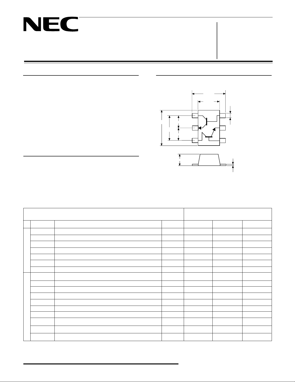
OUTLINE DIMENSIONS (Units in mm)
Package Outline TC
(TOP VIEW)
1.50±0.1
• LOW HEIGHT PROFILE:
Just 0.55 mm high
• FLAT LEAD STYLE:
Reduced lead inductance improves electrical
performance
• TWO DIFFERENT DIE TYPES:
Q1 - Ideal oscillator transistor
Q2 - Ideal buffer amplifier transistor
DESCRIPTION
The UPA836TC contains one NE685 and one NE688 NPN
1.50±0.1
0.48
0.96
0.48
0.55±0.05
1.10±0.1
1
2
34
+0.1
0.20
-0.05
6
5
+0.1
0.11
-0.05
high frequency silicon bipolar chip. NEC's new ultra small TC
package is ideal for all portable wireless applications where
reducing board space is a prime consideration. Each transistor
chip is independently mounted and easily configured for oscillator/buffer amplifier and other applications.
Note: Pin 1 is the lower left most pin
as the package lettering is oriented
and read left to right.
ELECTRICAL CHARACTERISTICS (TA = 25°C)
PART NUMBER UPA836TC
PACKAGE OUTLINE TC
SYMBOLS PARAMETERS AND CONDITIONS UNITS MIN TYP MAX
ICBO Collector Cutoff Current at VCB = 5 V, IE = 0 µA 0.1
IEBO Emitter Cutoff Current at VEB = 1 V, IC = 0 µA 0.1
hFE DC Current Gain1 at VCE = 3 V, IC = 10 mA 75 150
Q1
fT Gain Bandwidth at VCE = 3 V, IC = 10 mA, f = 2 GHz GHz 10 12
Cre Feedback Capacitance2 at VCB = 3 V, IE = 0, f = 1 MHz pF 0.4 0.7
2
|S21E|
NF Noise Figure at VCE = 3 V, IC = 3 mA, f = 2 GHz dB 1.5 2.5
ICBO Collector Cutoff Current at VCB = 5 V, IE = 0 µA 0.1
IEBO Emitter Cutoff Current at VEB = 1 V, IC = 0 µA 0.1
hFE DC Current Gain1 at VCE = 1 V, IC = 3 mA 80 160
fT Gain Bandwidth (1) at VCE = 1 V, IC = 3 mA, f = 2 GHz GHz 4.0 4.5
fT Gain Bandwidth (2) at VCE = 3 V, IC = 20 mA, f = 2 GHz GHz 9.0
Q2
Cre Feedback Capacitance2 at VCB = 1 V, IE = 0, f = 1 MHz pF 0.75 0.85
|S21E|
|S21E|
NF Noise Figure (1) at VCE = 1 V, IC = 3 mA, f = 2 GHz dB 1.7 2.5
NF Noise Figure (2) at VCE = 3 V, IC = 7 mA, f = 2 GHz dB 1.5
Insertion Power Gain at VCE = 3 V, IC =10 mA, f = 2 GHz dB 7 8.5
2
Insertion Power Gain (1) at VCE = 1 V, IC =3 mA, f = 2 GHz dB 2.5 3.5
2
Insertion Power Gain (2) at VCE = 3 V, IC =20 mA, f = 2 GHz dB 6.5
PIN OUT
1. Collector (Q1)
2. Emitter (Q1)
3. Collector (Q2)
4. Base (Q2)
5. Emitter (Q2)
6. Base (Q1)
Notes: 1. Pulsed measurement, pulse width ≤ 350 µs, duty cycle ≤ 2 %.
2. Collector to base capacitance when measured with capacitance meter (automatic balanced bridge method), with emitter connected to
guard pin of capacitances meter.
California Eastern Laboratories

UPA836TC
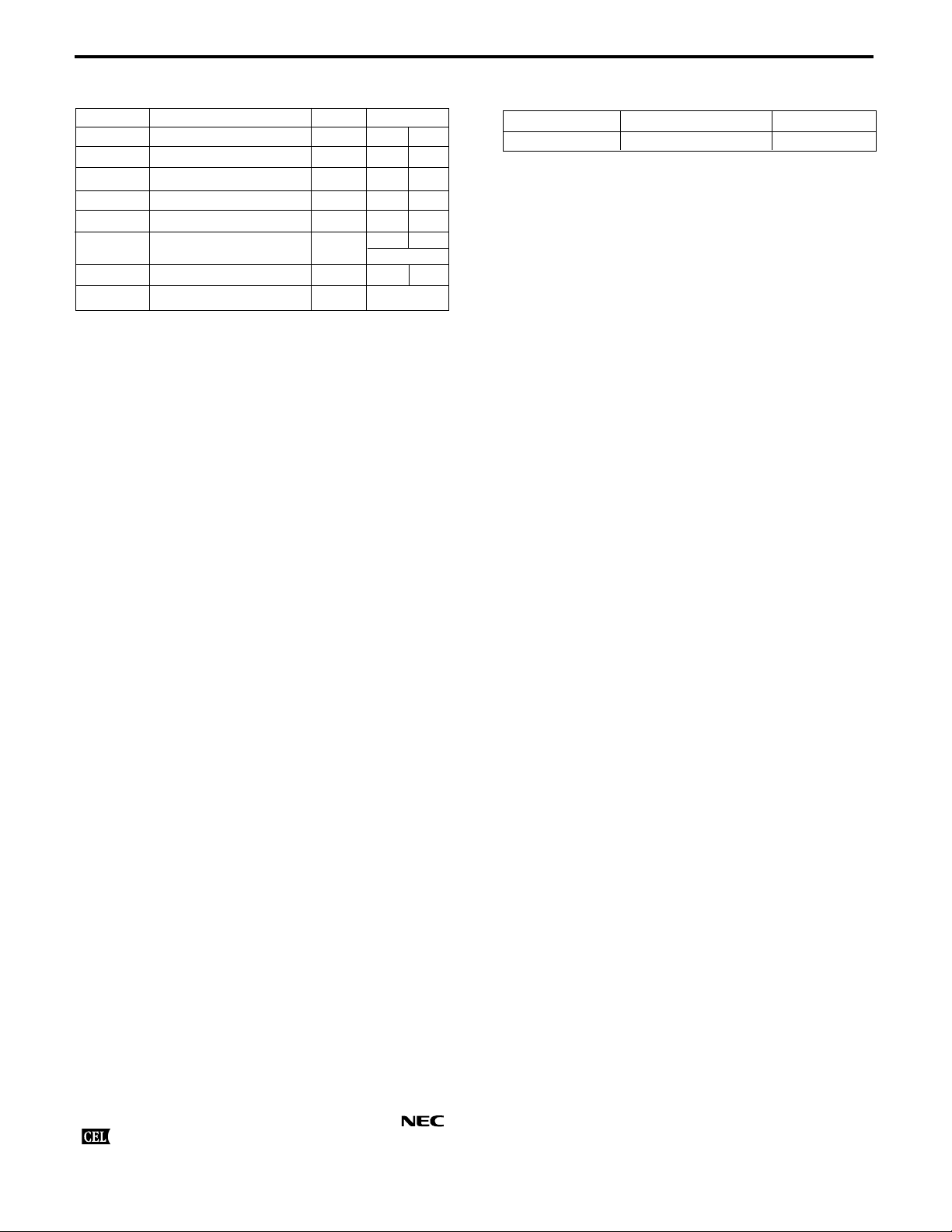
ABSOLUTE MAXIMUM RATINGS
1
(TA = 25°C)
SYMBOLS PARAMETERS UNITS RATINGS
Q1 Q2
CBO Collector to Base Voltage V
V
V
CEO Collector to Emitter Voltage V
VEBO Emitter to Base Voltage V
IC Collector Current mA
T Total Power Dissipation mW
P
9 9
6 6
2 2
30 100
TBD TBD
TBD
T
J Junction Temperature °C
STG Storage Temperature °C
T
150 150
-65 to +150
Note: 1. Operation in excess of any one of these parameters may
result in permanent damage.
ORDERING INFORMATION
PART NUMBER QUANTITY PACKAGING
UPA836TC-T1 3000 Tape & Reel
CALIFORNIA EASTERN LABORATORIES • Headquarters • 4590 Patrick Henry Drive • Santa Clara, CA 95054-1817 • (408) 988-3500 • Telex 34-6393 • FAX (408) 988-0279
DATA SUBJECT TO CHANGE WITHOUT NOTICE
EXCLUSIVE NORTH AMERICAN AGENT FOR RF, MICROWAVE & OPTOELECTRONIC SEMICONDUCTORS
24-Hour Fax-On-Demand: 800-390-3232 (U.S. and Canada only) • Internet: http://WWW.CEL.COM
1/99
 Loading...