


NEC uPD78F4218AYGF-3BA, uPD78F4218AGF-3BA, uPD78F4218AYGC-8EU, uPD78F4218AGC-8EU, uPD78F4216AYGF-3BA Datasheet
...
DATA SHEET
MOS INTEGRATED CIRCUIT
µµµµ
PD78F4216A, 78F4218A, 78F4216AY, 78F4218AY
16-BIT SINGLE-CHIP MICROCONTROLLERS
DESCRIPTION
The µPD78F4216A/78F4218A and 78F4216AY/78F4218AY are products of µPD784216A/784218A,
784216AY/784218AY Subseries in the 78K/IV Series.
The µPD78F4216A/78F4218A have flash memory in place of the internal ROM of the µPD784216A/784218A. The
incorporation of flash memory allows a program to be written or erased while mounted on the target board.
The µPD78F4216AY/78F4218AY are based on the µPD78F4216A/78F4218A Subseries with the addition of a
multimaster-supporting I2C bus interface.
Detailed function descriptions are provided in the following user’s manuals. Be sure to read them before
designing.
PD784216A, 784216AY Subseries User’s Manual Hardware: U13570E
µµµµ
PD784218A, 784218AY Subseries User’s Manual Hardware: U12970E
µµµµ
78K/IV Series User’s Manual Instructions: U10905E
FEATURES
Pin compatible with the mask ROM products
•
Flash memory: 128 KB (
•
256 KB (µPD78F4218A/78F4218AY)
Internal RAM: 8,192 bytes (µPD78F4216A/78F4216AY)
•
12,800 bytes (µPD78F4218A/78F4218AY)
Supply voltage: VDD = 1.9 to 5.5 V
•
PD78F4216A/78F4216AY)
µ
APPLICATIONS
Cellular phones, PHS, cordless telephones, CD-ROM, AV equipment
Unless otherwise specified, references in this document to the
78F4218A, 78F4216AY, and 78F4218AY.
PD78F4218AY refer to the
µµµµ
PD78F4216A,
µµµµ
The information in this document is subject to change without notice. Before using this document, please
confirm that this is the latest version.
Not all devices/types available in every country. Please check with local NEC representative for
availability and additional information.
Document No. U14125EJ1V0DS00 (1st edition)
Date Published November 2000 N CP(K)
Printed in Japan
2000

µµµµ
PD78F4216A, 78F4218A, 78F4216AY, 78F4218AY
ORDERING INFORMATION
Part Number Package Internal ROM (Bytes) Internal RAM (Bytes)
PD78F4216AGC-8EU 100-pin plastic LQFP
µ
(fine pitch) (14 × 14)
PD78F4216AGF-3BA 100-pin plastic QFP
µ
(14 × 20)
PD78F4218AGC-8EU 100-pin plastic LQFP
µ
(fine pitch) (14 × 14)
PD78F4218AGF-3BA 100-pin plastic QFP
µ
(14 × 20)
PD78F4216AYGC-8EU 100-pin plastic LQFP
µ
(fine pitch) (14 × 14)
128 K 8,192
128 K 8,192
256 K 12,800
256 K 12,800
128 K
8,192
PD78F4216AYGF-3BA 100-pin plastic QFP
µ
(14 × 20)
PD78F4218AYGC-8EU 100-pin plastic LQFP
µ
(fine pitch) (14 × 14)
PD78F4218AYGF-3BA 100-pin plastic QFP
µ
(14 × 20)
128 K
256 K 12,800
256 K 12,800
8,192
2
Data Sheet U14125EJ1V0DS00
78K/IV SERIES LINEUP
: Products in mass-production
: Products under development
Standard models
PD784026
µ
Enhanced
A/D converter,
16-bit timer, and
power management
ASSP models
PD784956A
µ
For DC inverter control
PD784908
µ
On-chip IEBus
PD784915
µ
Software servo control
On-chip analog circuit for VCRs
Enhanced timer
TM
controller
µµµµ
PD78F4216A, 78F4218A, 78F4216AY, 78F4218AY
2
Supports I
µ
µ
PD784038
Enhanced internal memory capacity
Pin-compatible with the PD784026
Supports multimaster I2C bus
µ
PD784216AY
µ
PD784216A
100-pin, enhanced I/O and
internal memory capacity
µ
PD784046
On-chip 10-bit A/D converter
µ
PD784938A
Enhanced functions of the
µ
PD784908, enhanced
internal memory capacity,
ROM correction added.
Supports multimaster I
µ
PD784928
µ
Enhanced functions
of the PD784915
C bus
PD784038Y
µ
PD784054
PD784928Y
µ
2
C bus
Supports multimaster I
µ
PD784225Y
µ
PD784225
µ
80-pin, ROM correction added
Supports multimaster I
µ
PD784218AY
µ
PD784218A
Enhanced internal memory
capacity, ROM correction added
µ
PD784967
Enhanced functions of the
µ
PD784938A, enhanced
I/O and internal memory
capacity.
2
C bus
2
C bus
PD784976
µ
On-chip VFD controller/driver
Data Sheet U14125EJ1V0DS00
3
µµµµ
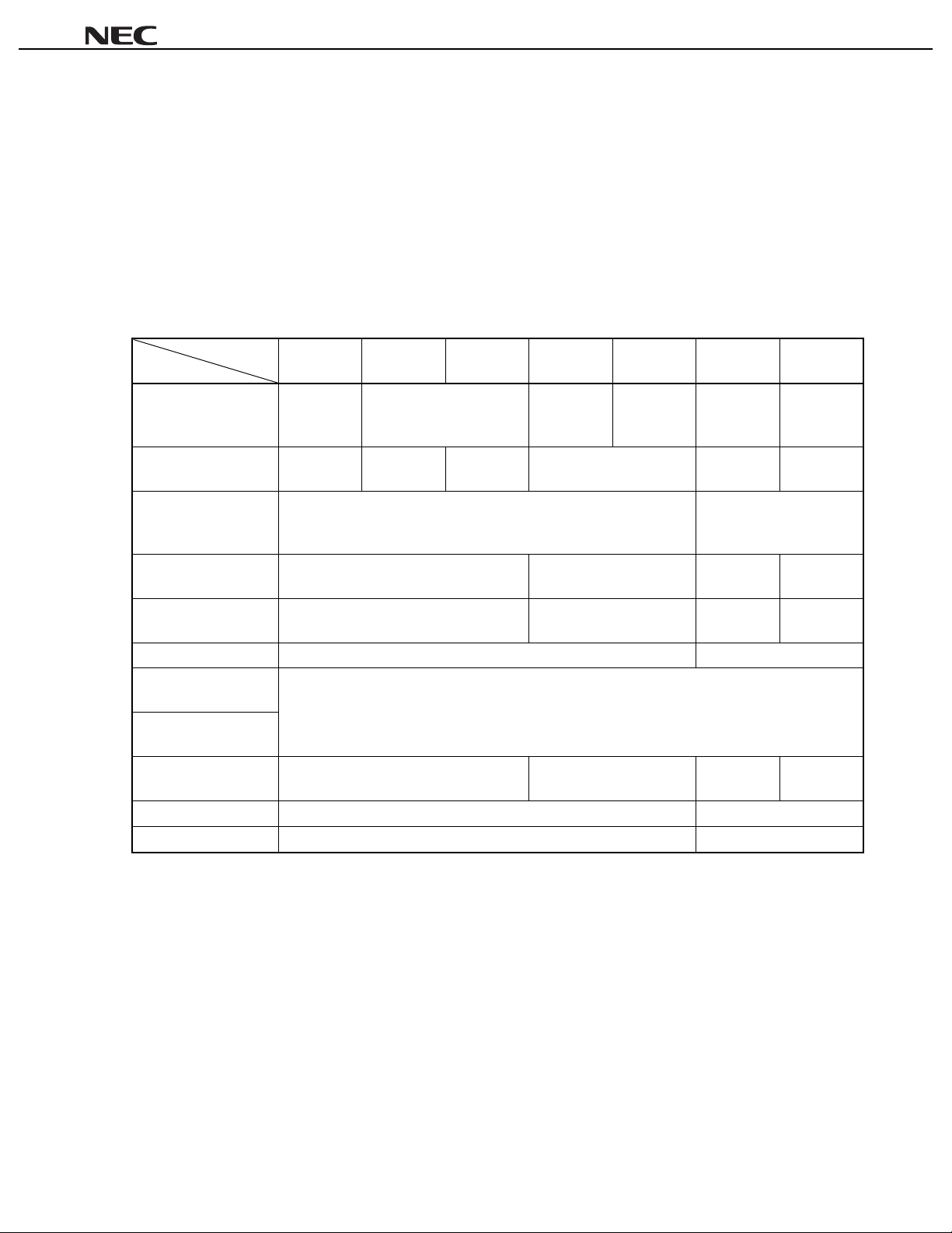
OVERVIEW OF FUNCTIONS (1/2)
PD78F4216A, 78F4218A, 78F4216AY, 78F4218AY
Part Number
Item
Number of basic instruc t i ons (mnemonics) 113
General-purpose registers 8 bits × 16 registers × 8 banks, or 16 bits × 8 registers × 8 banks (memory
mapping)
Minimum instructi on execution time
Flash memory 128 KB 256 KBInternal
memory
Memory space 1 MB with program and data spaces combined
I/O ports
Pins with
additional
functions
Real-time output port 4 bits × 2 or 8 bits × 1
Timer/event counter
Serial interface
A/D converter 8-bit resolution × 8 channels
D/A converter 8-bit resolution × 2 channels
Note 1
RAM 8,192 bytes 12,800 bytes
Total 86
CMOS input 8
CMOS I/O 72
N-ch open-drain I/O 6
Pins with pull-up resistor 70
LED direct drive output 22
Middle-voltage pin 6
160 ns/320 ns/640 ns/1,280 ns/2,560 ns (@fXX = 12.5 MHz operation with
•
main system clock)
61
•
µ
Timer/event counter: Timer counter × 1 Pulse output
(16-bit) Capture/compare register × 2 • PPG output
Timer/event counter 1: Timer counter × 1 Pulse output
(8-bit) Compare register
Timer/event counter 2: Timer counter × 1 Pulse output
(8-bit) Compare register
Timer/event counter 5: Timer counter × 1 Pulse output
(8-bit) Compare register
Timer/event counter 6: Timer counter × 1 Pulse output
(8-bit) Compare register
Timer/event counter 7: Timer counter × 1 Pulse output
(8-bit) Compare register
Timer/event counter 8: Timer counter × 1 Pulse output
(8-bit) Compare register
UART/IOE (3-wire serial I/O): 2 channels (on-chip baud rate generat or)
•
CSI (3-wire serial I / O , multimaster support i ng I
•
PD78F4216A,
µ
PD78F4216AY
µ
s (@fXT = 32.768 kHz operation with subsystem clock)
1
×
1
×
1
×
1
×
1
×
1
×
PD78F4218A,
µ
PD78F4218AY
µ
Square wave output
•
One-shot pulse output
•
PWM output
•
Square wave output
•
PWM output
•
Square wave output
•
PWM output
•
Square wave output
•
PWM output
•
Square wave output
•
PWM output
•
Square wave output
•
PWM output
•
Square wave output
•
2
Note 2
C bus
): 1 channel
Notes 1.
4
Pins with additional functions are included with the I/O pins.
PD78F4216AY, 78F4218AY only
2.
µ
Data Sheet U14125EJ1V0DS00
OVERVIEW OF FUNCTIONS (2/2)
µµµµ
PD78F4216A, 78F4218A, 78F4216AY, 78F4218AY
Item
Clock output
Buzzer output
Watch timer
Watchdog timer
Standby
Interrupt
Supply voltage
Package
Part Number
Selectable from f
Selectable from f
PD78F4216A,
µ
PD78F4216AY
µ
XX
, fXX/2, fXX/22, fXX/23, fXX/24, fXX/25, fXX/26, fXX/27, f
XX
/210, fXX/211, fXX/212, fXX/2
13
1 channel
1 channel
HALT/STOP/IDLE modes
•
In low power consumption m ode (wi th subsystem clock): HALT/IDLE modes
•
Hardware sources 29 (i nternal: 20, external: 9)
Software sources BRK instruction, BRKCS instruction, operand error
Non-maskable Internal: 1, external: 1
Maskable Internal: 19, external: 8
4 programmable priority lev el s
•
3 service modes: V ectored interrupt/macro serv ice/context switc hi ng
•
DD
V
= 1.9 to 5.5 V
100-pin plastic LQFP (fine pitch) (14 × 14)
100-pin plastic QFP (14 × 20)
PD78F4218A,
µ
PD78F4218AY
µ
XT
Data Sheet U14125EJ1V0DS00
5

µµµµ
PD78F4216A, 78F4218A, 78F4216AY, 78F4218AY
CONTENTS
1. DIFFERENCES AMONG MODELS IN
SUBSERIES.............................................................................................................................................7
2. PIN CONFIGURATION (TOP VIEW)...................................................................................................8
3. BLOCK DIAGRAM...............................................................................................................................11
4. PIN FUNCTIONS..................................................................................................................................12
4.1 Port Pins .....................................................................................................................................12
4.2 Non-Port Pins .............................................................................................................................14
4.3 Pin I/O Circuits and Recommended Connections of Unused Pins .......................................16
5. INTERNAL MEMORY SIZE SWITCHING REGISTER (IMS)................................................................20
6. PROGRAMMING FLASH MEMORY.....................................................................................................22
6.1 Selecting Communication Mode ..............................................................................................22
6.2 Flash Memory Programming Function ....................................................................................23
6.3 Connecting Flashpro ll and Flashpro lll...................................................................................24
7. ELECTRICAL SPECIFICATIONS ........................................................................................................25
PD784216A/784216AY, 784218A/784218AY
µµµµ
8. PACKAGE DRAWINGS.......................................................................................................................47
9. RECOMMENDED SOLDERING CONDITIONS..................................................................................49
APPENDIX A. DEVELOPMENT TOOLS ................................................................................................50
APPENDIX B. RELATED DOCUMENTS................................................................................................53
6
Data Sheet U14125EJ1V0DS00
µµµµ
PD78F4216A, 78F4218A, 78F4216AY, 78F4218AY
1. DIFFERENCES AMONG MODELS IN
PD784216A/784216AY, 784218A/784218AY SUBSERIES
µµµµ
The only difference among the µPD784214A, 784215A, 784216A, 784217A, and 784218A lies in the internal
memory capacity.
The µPD784214AY, 784215AY, 784216AY, 784217AY, and 784218AY are models with the addition of an I2C bus
control function.
The µPD78F4216A, 78F4216AY, 78F4218A, and 78F4218AY are provided with a 128 KB/256 KB flash memory
instead of the mask ROM of the above models.
These differences are summarized in Table 1-1.
Table 1-1. Differences Among Models in
PD784214A,
Part Number
Item
Internal ROM 96 KB
Internal RAM 3,584 bytes 5,120 bytes 8,192 bytes 12,800 bytes 8,192
Internal memory size
switching register
(IMS)
ROM correction Not provided Provided Not
External access status
function
Supply voltage VDD = 1.8 to 5.5 V VDD = 1.9 to 5.5 V
Electrical
specifications
Recommended
soldering conditions
EXA pin Not provided Provided Not
TEST pin Provided Not provided
VPP pin Not provided Provided
µ
PD784214AY
µ
(Mask
ROM)
Not provided
Not provided Provided Not
Refer to the data sheet for each device.
PD784215A,
µ
PD784215AY
µ
128 KB (Mask ROM) 192 KB
PD784216A/784216AY, 784218A/784218AY Subseries
µµµµ
µ
PD784216A,
µ
PD784216AY
µ
PD784217A,
µ
PD784217AY
µ
(Mask
ROM)
PD784218A,
µ
PD784218AY
µ
256 KB
(Mask
ROM)
PD78F4216A,
µ
PD78F4216AY
128 KB
(Flash
memory)
bytes
Provided
provided
provided
provided
µ
256 KB
(Flash
memory)
12,800
bytes
Note
Provided
Provided
Provided
µ
PD78F4218A,
PD78F4218AY
The internal flash memory capacity and internal RAM capacity can be changed using the internal memory
Note
size switching register (IMS).
Caution There are differences in noise immunity and noise radiation between the flash memory and mask
ROM versions. When pre-producing an application set with the flash memory version and then
mass-producing it with the mask ROM version, be sure to conduct sufficient evaluations on the
commercial samples (not engineering samples) of the mask ROM version.
Data Sheet U14125EJ1V0DS00
7
µµµµ
PD78F4216A, 78F4218A, 78F4216AY, 78F4218AY
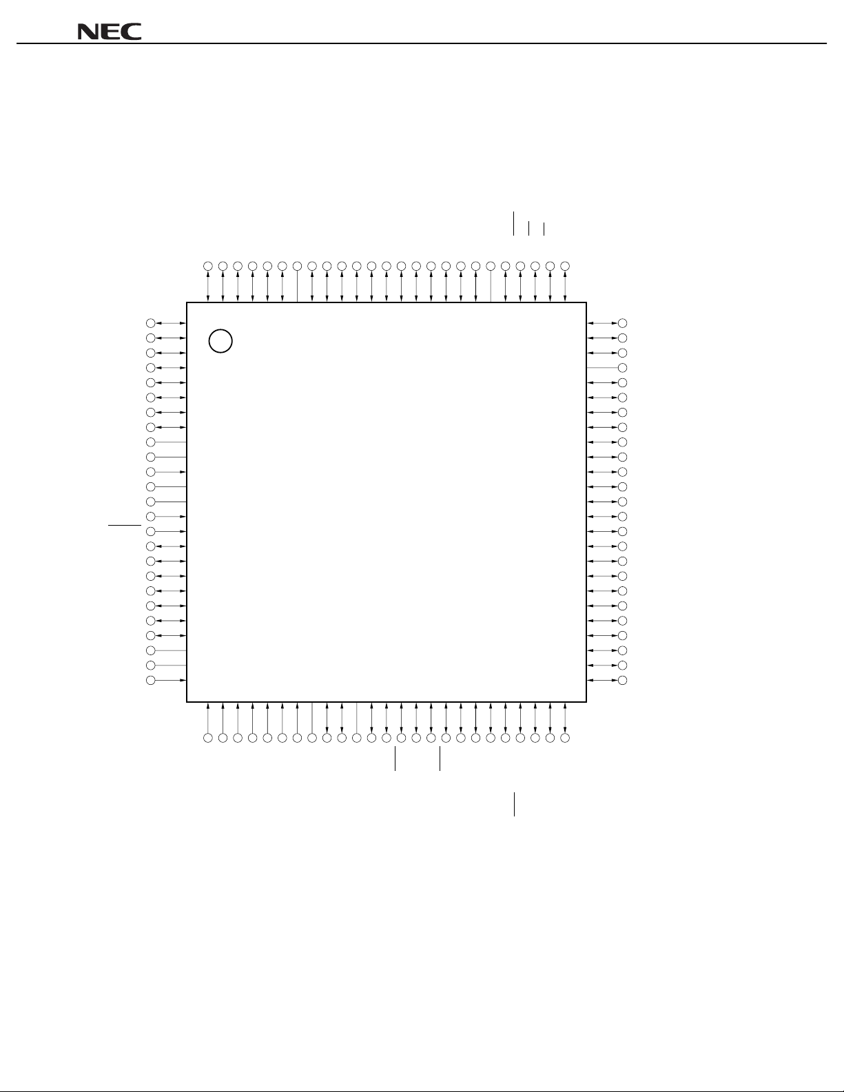
2. PIN CONFIGURATION (TOP VIEW)
100-pin plastic LQFP (fine pitch) (14
••••
PD78F4216AGC-8EU,
µµµµ
P95
P94
100 76
P120/RTP0
P121/RTP1
P122/RTP2
P123/RTP3
P124/RTP4
P125/RTP5
P126/RTP6
P127/RTP7
V
X2
X1
V
XT2
XT1
RESET
P00/INTP0
P01/INTP1
P02/INTP2/NMI
P03/INTP3
P04/INTP4
P05/INTP5
P06/INTP6
Note 2
AV
DD
AV
REF0
P10/ANI0
DD
SS
1
2
3
4
5
6
7
8
9
10
11
12
13
14
15
16
17
18
19
20
21
22
23
24
25
26 504948474645444342414039383736353433323130292827
14)
××××
PD78F4218AGC-8EU,
µµµµ
Note 5
Note 1
P91
P90
PP
V
P37/EXA
P36/TI01
P35/TI00
P93
P92
PD78F4216AYGC-8EU,
µµµµ
P34/TI2
P33/TI1
P32/TO2
P31/TO1
P30/TO0
P103/TI8/TO8
P102/TI7/TO7
P101/TI6/TO6
P100/TI5/TO5
VDDP67/ASTB
PD78F4218AYGC-8EU
µµµµ
P66/WAIT
P65/WR
P64/RD
P63/A19
7778798081828384858687888990919293949596979899
75
74
73
72
71
70
69
68
67
66
65
64
63
62
61
60
59
58
57
56
55
54
53
52
51
P62/A18
P61/A17
P60/A16
V
P57/A15
P56/A14
P55/A13
P54/A12
P53/A11
P52/A10
P51/A9
P50/A8
P47/AD7
P46/AD6
P45/AD5
P44/AD4
P43/AD3
P42/AD2
P41/AD1
P40/AD0
P87/A7
P86/A6
P85/A5
P84/A4
P83/A3
SS
Notes 1.
8
REF1
AV
P130/ANO0
P131/ANO1
P70/RxD2/SI2
P20/RxD1/SI1
P71/TxD2/SO2
P72/ASCK2/SCK2
Note 4
P23/PCL
P24/BUZ
P21/TxD1/SO1
P22/ASCK1/SCK1
Note 4
P80/A0
P26/SO0
P25/SI0/SDA0
P27/SCK0/SCL0
P81/A1
P82/A2
P11/ANI1
Connect the V
Note 3
SS
P12/ANI2
P13/ANI3
P14/ANI4
P15/ANI5
PP
pin to VSS directly or via a pull-down resistor in normal operation mode. Connect the
AV
P16/ANI6
P17/ANI7
VPP pin to VSS via a pull-down resistor in a system in which the on-chip flash memory is written while
mounted on the target board. For the pull-down connection, it is recommended to use a resistor with a
resistance ranging from 470 Ω to 10 kΩ.
Connect the AVDD pin to VDD.
2.
Connect the AVSS pin to VSS.
3.
The SCL0 and SDA0 pins are available in the µPD78F4216AY, 78F4218AY only.
4.
The EXA pin is available in the µPD78F4218A, 78F4218AY only.
5.
Data Sheet U14125EJ1V0DS00
µµµµ
PD78F4216A, 78F4218A, 78F4216AY, 78F4218AY
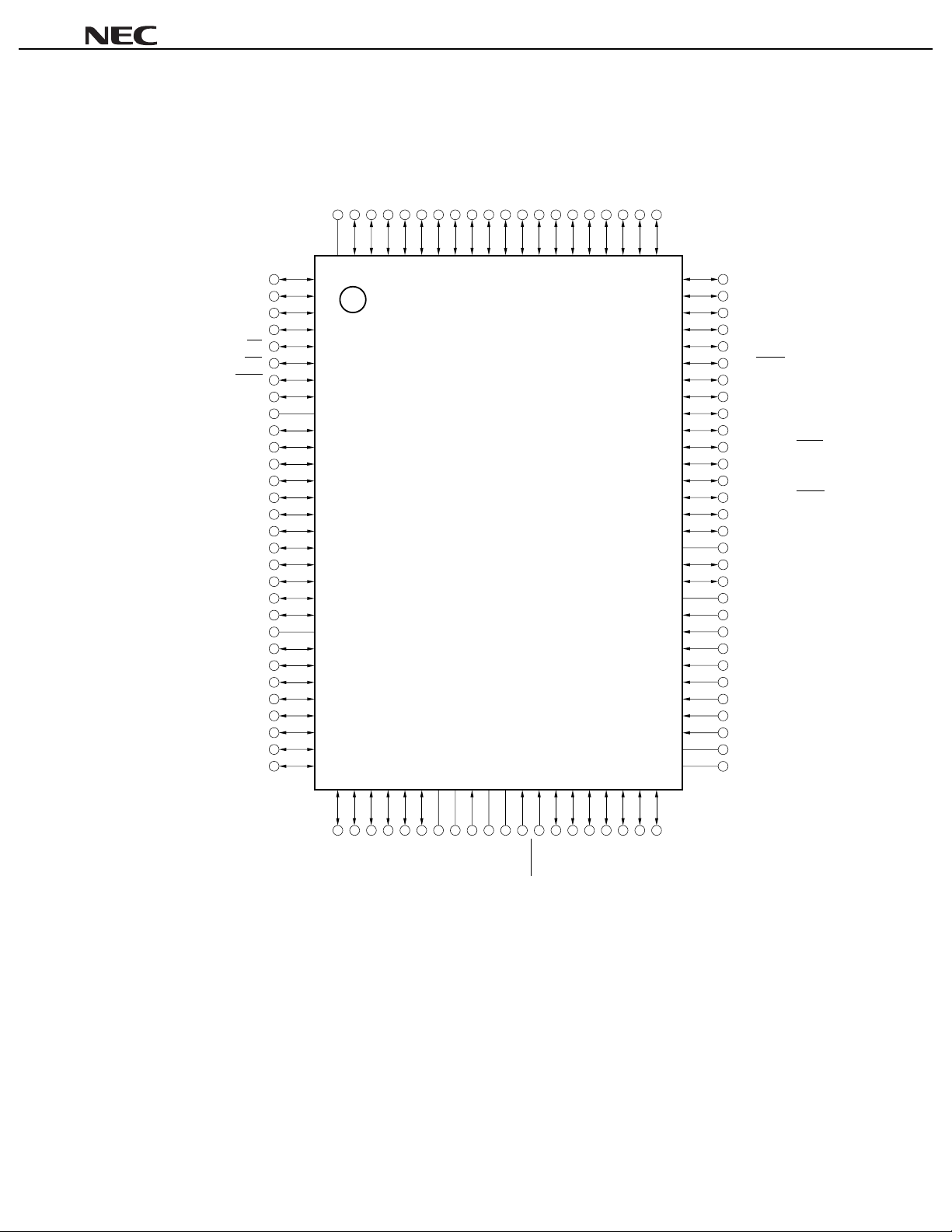
100-pin plastic QFP (14
••••
PD78F4216AGF-3BA,
µµµµ
P60/A16
P61/A17
P62/A18
P63/A19
P64/RD
P65/WR
P66/WAIT
P67/ASTB
V
DD
P100/TI5/TO5
P101/TI6/TO6
P102/TI7/TO7
P103/TI8/TO8
P30/TO0
P31/TO1
P32/TO2
P33/TI1
P34/TI2
P35/TI00
P36/TI01
Note 5
P37/EXA
Note 1
V
PP
P90
P91
P92
P93
P94
P95
P120/RTP0
P121/RTP1
20)
××××
PD78F4218AGF-3BA,
µµµµ
VSSP57/A15
P56/A14
P55/A13
P54/A12
P53/A11
100
1
2
3
4
5
6
7
8
9
10
11
12
13
14
15
16
17
18
19
20
21
22
23
24
25
26
27
28
29
30
31 50494847464544434241403938373635343332
PD78F4216AYGF-3BA,
µµµµ
P52/A10
P51/A9
P50/A8
P47/AD7
P46/AD6
P45/AD5
P44/AD4
P43/AD3
P42/AD2
PD78F4218AYGF-3BA
µµµµ
P41/AD1
P40/AD0
P87/A7
P86/A6
P85/A5
81828384858687888990919293949596979899
80
79
78
77
76
75
74
73
72
71
70
69
68
67
66
65
64
63
62
61
60
59
58
57
56
55
54
53
52
51
P84/A4
P83/A3
P82/A2
P81/A1
P80/A0
P27/SCK0/SCL0
P26/SO0
P25/SI0/SDA0
P24/BUZ
P23/PCL
P22/ASCK1/SCK1
P21/TxD1/SO1
P20/RxD1/SI1
P72/ASCK2/SCK2
P71/TxD2/SO2
P70/RxD2/SI2
AV
REF1
P131/ANO1
P130/ANO0
Note 3
AV
SS
P17/ANI7
P16/ANI6
P15/ANI5
P14/ANI4
P13/ANI3
P12/ANI2
P11/ANI1
P10/ANI0
AV
REF0
Note 2
AV
DD
Note 4
Note 4
Notes 1.
X2
X1
SS
V
XT2
XT1
RESET
P00/INTP0
P01/INTP1
P03/INTP3
P04/INTP4
P05/INTP5
P06/INTP6
P02/INTP2/NMI
Connect the V
DD
V
P122/RTP2
P123/RTP3
P124/RTP4
P125/RTP5
P126/RTP6
P127/RTP7
PP
pin to VSS directly or via a pull-down resistor in normal operation mode. Connect the
VPP pin to VSS via a pull-down resistor in a system in which the on-chip flash memory is written while
mounted on the target board. For the pull-down connection, it is recommended to use a resistor with a
resistance ranging from 470 Ω to 10 kΩ.
Connect the AVDD pin to VDD.
2.
Connect the AVSS pin to VSS.
3.
The SCL0 and SDA0 pins are available in the µPD78F4216AY, 78F4218AY only.
4.
The EXA pin is available in the µPD78F4218A, 78F4218AY only.
5.
Data Sheet U14125EJ1V0DS00
9

µµµµ
PD78F4216A, 78F4218A, 78F4216AY, 78F4218AY
A0 to A19: Address Bus P120 to P127: Port 12
AD0 to AD7: Address/Data Bus P130, P131: Port 13
ANI0 to ANI7: Analog Input PCL: Programmable Clock
ANO0, ANO1: Analog Output RD: Read Strobe
ASCK1, ASCK2: Asynchronous Serial Clock RESET: Reset
ASTB: Address Strobe RTP0 to RTP7: Real-time Output Port
AVDD: Analog Power Supply RxD1, RxD2: Receive Data
REF0
AV
AVSS: Analog Ground SCL0
BUZ: Buzzer Clock SDA0
EXA
INTP0 to INTP6: Interrupt from Peripherals SO0 to SO2: Serial Output
NMI: Non-maskable Interrupt TI00, TI01,
P00 to P06: Port 0 TI1, TI2, TI5 to TI8: Timer Input
P10 to P17: Port 1 TO0 to TO2, TO5 to TO8: Timer Output
P20 to P27: Port 2 TxD1, TxD2: Transmit Data
P30 to P37: Port 3 VDD: Power Supply
P40 to P47: Port 4 VPP: Programming Power Supply
P50 to P57: Port 5 VSS: Ground
P60 to P67: Port 6 WAIT: Wait
P70 to P72: Port 7 WR: Write Strobe
P80 to P87: Port 8 X1, X2: Crystal (Main System Clock)
P90 to P95: Port 9 XT1, XT2: Crystal (Subsystem Clock)
P100 to P103: Port 10
REF1
, AV
Note 2
: Analog Reference Voltage SCK0 to SCK2: Serial Clock
Note 1
: Serial Clock
Note 1
: Serial Data
: External Access Status Output SI0 to SI2: Serial Input
Notes 1.
The SCL0 and SDA0 pins are available in the µPD78F4216AY, 78F4218AY only.
The EXA pin is available in the µPD78F4218A, 78F4218AY only.
2.
10
Data Sheet U14125EJ1V0DS00
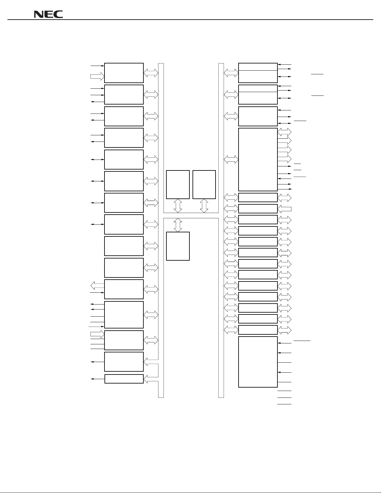
3. BLOCK DIAGRAM
µµµµ
PD78F4216A, 78F4218A, 78F4216AY, 78F4218AY
INTP2/NMI
INTP0, INTP1,
INTP3 to INTP6
TI00
TI01
TO0
TI1
TO1
TI2
TO2
TI5/TO5
TI6/TO6
TI7/TO7
TI8/TO8
RTP0 to RTP7
NMI/INTP2
ANO0
ANO1
REF1
AV
AV
SS
P03/INTP3
ANI0 to ANI7
AV
REF0
AV
DD
AV
SS
PCL
BUZ
Programmable
interrupt
controller
Timer/event
counter
(16 bits)
Timer/event
counter 1
(8 bits)
Timer/event
counter 2
(8 bits)
Timer/event
counter 5
(8 bits)
Timer/event
counter 6
(8 bits)
Timer/event
counter 7
(8 bits)
Timer/event
counter 8
(8 bits)
Watch timer
Watchdog timer
Real-time
output port
D/A
converter
A/D
converter
Clock output
control
Buzzer output
78K/IV
CPU core
RAM
Flash
memory
UART/IOE1
Baud-rate
generator
UART/IOE2
Baud-rate
generator
Clocked
serial
interface
Bus I/F
Port 0
Port 1
Port 2
Port 3
Port 4
Port 5
Port 6
Port 7
Port 8
Port 9
Port 10
Port 12
Port 13
System control
RxD1/SI1
TxD1/SO1
ASCK1/SCK1
RxD2/SI2
TxD2/SO2
ASCK2/SCK2
SI0/SDA0
Note 1
SO0
SCK0/SCL0
AD0 to AD7
A0 to A7
A8 to A15
A16 to A19
RD
WR
WAIT
ASTB
Note 2
EXA
P00 to P06
P10 to P17
P20 to P27
P30 to P37
P40 to P47
P50 to P57
P60 to P67
P70 to P72
P80 to P87
P90 to P95
P100 to P103
P120 to P127
P130, P131
RESET
X1
X2
XT1
XT2
V
DD
V
SS
V
PP
Note 1
Notes 1.
2
This function supports the I
The EXA pin is available in the µPD78F4218A, 78F4218AY only.
2.
C bus interface and is available in the µPD78F4216AY, 78F4218AY only.
Data Sheet U14125EJ1V0DS00
11
µµµµ
PD78F4216A, 78F4218A, 78F4216AY, 78F4218AY
4. PIN FUNCTIONS
4.1 Port Pins (1/2)
Pin Name I / O Alternate Function Function
P00 INTP0
P01 INTP1
P02 INTP2/NMI
P03 INTP3
P04 INTP4
P05 INTP5
P06
P10 to P17 Input ANI0 to ANI7 Port 1 (P1):
P20 RxD1/SI1
P21 TxD1/SO1
P22 ASCK1/SCK1
P23 PCL
P24 BUZ
P25 SI0/SDA0
P26 SO0
P27
P30 TO0
P31 TO1
P32 TO2
P33 TI1
P34 TI2
P35 TI00
P36 TI01
P37
P40 to P47 I/O AD0 to AD7 Port 4 (P4):
P50 to P57 I/O A8 to A15 Port 5 (P5):
I/O
I/O
I/O
INTP6
SCK0/SCL0
Note 2
EXA
Note 1
Note 1
Port 0 (P0):
7-bit I/O port
•
Input/output can be spec i f i ed i n 1-bi t units.
•
Whether specifying input m ode or output mode, an on-chip pull-up
•
resistor can be specif i ed i n 1-bi t units by means of sof tware.
8-bit input only port
•
Port 2 (P2):
8-bit I/O port
•
Input/output can be specified in 1-bit uni t s.
•
Whether specifying input mode or output mode, an on-c hi p pul l -up
•
resistor can be specif i ed i n 1-bi t units by means of sof tware.
Port 3 (P3):
8-bit I/O port
•
Input/output can be specified in 1-bit uni t s.
•
Whether specifying input mode or output mode, an on-c hi p pul l -up
•
resistor can be specif i ed i n 1-bi t units by means of sof tware.
8-bit I/O port
•
Input/output can be specified in 1-bit uni t s.
•
When used as an input port, an on-chip pull-up resistor c an be
•
specified by means of s oftware.
LEDs can be driven directly.
•
8-bit I/O port
•
Input/output can be specified in 1-bit uni t s.
•
When used as an input port, an on-chip pull -up resistor can be
•
specified by means of s oftware.
LEDs can be driven directly.
•
Notes 1.
12
This SDA0 and SCL0 are available in the
This function is available in the µPD78F4218A, 784218AY only.
2.
Data Sheet U14125EJ1V0DS00
PD78F4216AY, 78F4218AY only.
µ
µµµµ
PD78F4216A, 78F4218A, 78F4216AY, 78F4218AY
4.1 Port Pins (2/2)
Pin Name I / O Alternate Function Function
P60 A16
P61 A17
P62 A18
P63 A19
P64 RD
P65 WR
P66 WAIT
P67
P70 RxD2/SI2
P71 TxD2/SO2
P72
P80 to P87 I/O A0 to A7 Port 8 (P8):
P90 to P95 I/O
P100 TI5/TO5
P101 TI6/TO6
P102 TI7/TO7
P103
P120 to P127 I/O RTP0 to RTP7 P ort 12 (P12):
P130, P131 I/O ANO0, ANO1 Port 13 (P13):
I/O
I/O
I/O
ASTB
ASCK2/SCK2
−
TI8/TO8
Port 6 (P6):
8-bit I/O port
•
Input/output can be specified in 1-bit uni t s.
•
When used as an input port, an on-chip pull -up resistor can be
•
specified by means of s oftware.
Port 7 (P7):
3-bit I/O port
•
Input/output can be specified in 1-bit uni t s.
•
Whether specifying input mode or output mode, an on-c hi p pul l -up
•
resistor can be specif i ed i n 1-bi t units by means of sof tware.
8-bit I/O port
•
Input/output can be specified in 1-bit uni t s.
•
Whether specifying input mode or output mode, an on-c hi p pul l -up
•
resistor can be specif i ed i n 1-bi t units by means of sof tware.
The interrupt control flag (KRIF) is set t o 1 when a falling edge is
•
detected at a pin of this port .
Port 9 (P9):
N-ch open-drain middle-voltage I/O port
•
6-bit I/O port
•
Input/output can be specified in 1-bit uni t s.
•
LEDs can be driven directly.
•
Port 10 (P10):
4-bit I/O port
•
Input/output can be specified in 1-bit uni t s.
•
Whether specifying input mode or output mode, an on-c hi p pul l -up
•
resistor can be specif i ed i n 1-bi t units by means of sof tware.
8-bit I/O port
•
Input/output can be specified in 1-bit uni t s.
•
Whether specifying input mode or output mode, an on-c hi p pul l -up
•
resistor can be specif i ed i n 1-bi t units by means of sof tware.
2-bit I/O port
•
Input/output can be specified in 1-bit uni t s.
•
Data Sheet U14125EJ1V0DS00
13
µµµµ
PD78F4216A, 78F4218A, 78F4216AY, 78F4218AY
4.2
Non-Port Pins (1/2)
Pin Name I / O Alternate Function Function
TI00 P35 External count c l ock input to 16-bit timer c ounter
TI01 P36 Capture trigger signal input to capture/compare register 00
TI1 P33 External count c l ock input to 8-bit timer c ounter 1
TI2 P34 External count c l ock input to 8-bit timer c ounter 2
TI5 P100/TO5 External count clock input t o 8-bi t timer counter 5
TI6 P101/TO6 External count clock input t o 8-bi t timer counter 6
TI7 P102/TO7 External count clock input t o 8-bi t timer counter 7
TI8
TO0 P30 16-bit timer output (shared by 14-bit PWM output)
TO1 P31
TO2 P32
TO5 P100/TI5
TO6 P101/TI6
TO7 P102/TI7
TO8
RxD1 P20/SI1 Serial data input (UART1)
RxD2
TxD1 P21/SO1 Serial data output (UART1)
TxD2
ASCK1 P22/SCK1 Baud rate clock input (UA RT1)
ASCK2
SI0 P25/SDA0
SI1 P20/RxD1 Serial data input (3-wi re serial I/O 1)
SI2
SO0 P26 Serial data output (3-wire s eri al I/O 0)
SO1 P21/TxD1 S eri al data output (3-wire serial I/O 1)
SO2
Note
SDA0
SCK0 P27/SCL0
SCK1 P22/ASCK1 S eri al c l ock input/output (3-wire serial I/O 1)
SCK2 P72/ASCK2 S eri al c l ock input/output (3-wire serial I/O 2)
Note
SCL0
NMI P02/INTP2 Non-maskable interrupt request input
INTP0 P00
INTP1 P01
INTP2 P02/NMI
INTP3 P03
INTP4 P04
INTP5 P05
INTP6
Input
Output
Input
Output
Input
Input
Output
I/O
Input
P103/TO8 External count clock input t o 8-bi t timer counter 8
8-bit timer output (shared by 8-bi t PWM output)
P103/TI8
P70/SI2 Serial data input (UA RT2)
P71/SO2 Serial data output (UA RT2)
P72/SCK2 Baud rate cl ock input (UART2)
Note
P70/RxD2 Serial data input (3-wire serial I /O 2)
P71/TxD2 S eri al data output (3-wire serial I/O 2)
P25/SI0 Serial data input/output (I2C bus)
Note
P27/SCK0 Serial c l ock input/output (I
P06
Serial data input (3-wire serial I /O 0)
Serial clock input/ output (3-wire serial I/O 0)
2
C bus)
External interrupt request i nput
14
This function is available in the
Note
PD78F4216AY, 78F4218AY only.
µ
Data Sheet U14125EJ1V0DS00
µµµµ
PD78F4216A, 78F4218A, 78F4216AY, 78F4218AY
4.2 Non-Port Pins (2/2)
Pin Name I / O Alternate Function Function
PCL Output P23 Clock output (for trimming main system clock and subsystem clock)
BUZ Output P24 Buzzer out put
RTP0 to RTP7 Output P120 to P127 Real-time output port that out put s data in synchronizati on wi t h
trigger
AD0 to AD7 I/O P40 to P47 Lower address/data bus for expanding memory externally
A0 to A7 P80 to P87 Lower addres s bus for expanding memory external l y
A8 to A15 P50 to P57 Mi ddl e address bus for expanding memory ex t ernal l y
A16 to A19
RD P64 Strobe signal output f or readi ng from external memory
WR
WAIT Input P66 Wait insertion at external memory access
ASTB Output P67 Strobe output that external l y latches address inform at i on output to
Note
EXA
RESET Input
X1 Input
X2
XT1 Input
XT2
ANI0 to ANI7 Input P10 t o P17 A/D converter analog input
ANO0, ANO1 Output P130, P131 D/A converter analog output
REF0
AV
REF1
AV
DD
AV
SS
AV
DD
V
SS
V
PP
V
Output
P60 to P63 Higher addres s bus for expanding memory ext ernal l y
Output
P65 Strobe signal output for writing to external memory
ports 4 through 6 and 8 to access external memory
Output P37 Status signal output at external memory access
−
−
System reset input
Connecting crystal res onator for main system clock oscillation
−
−
Connecting crystal res onator for subsystem clock oscillation
−
−−
A/D converter reference v ol t age i nput
D/A converter reference v ol t age i nput
A/D converter positi ve power supply. Connect to VDD.
GND for A/D converter and D/A converter. Connect to VSS.
Positive power supply
GND
Flash memory programming mode setting.
Applying high-voltage for program wri te/verify. Connect t hi s pin to
SS
directly or via a pull-down res i s tor in normal operation mode.
V
Connect the V
PP
pin to VSS via a pull-down resistor in a system in
which the on-chip flash mem ory is written while mounted on the
target board. For the pull-down connect i on, it is recommended to
use a resistor with a resistance ranging from 470 Ω to 10 kΩ.
The EXA pin is available in the
Note
PD78F4218A, 78F4218AY only.
µ
Data Sheet U14125EJ1V0DS00
15
µµµµ
PD78F4216A, 78F4218A, 78F4216AY, 78F4218AY
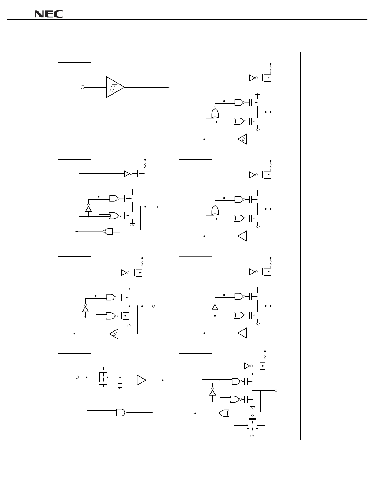
4.3 Pin I/O Circuits and Recommended Connections of Unused Pins
The I/O circuit type of each pin and recommended connections of unused pins are shown in Table 4-1.
For each type of input/output circuit, refer to Figure 4-1.
Table 4-1. Types of Pin I/O Circuits and Recommended Connection of Unused Pins (1/2)
Pin Name I/O Circuit Type I/O Recommended Connection of Unused Pi ns
P00/INTP0
P01/INTP1
P02/INTP2/NMI
P03/INTP3 to P06/INTP6
P10/ANI0 to P17/ANI7 9 Input Connect to VSS or V
P20/RxD1/SI1 10-K
P21/TxD1/SO1 10-L
P22/ASCK1/SCK1 10-K
P23/PCL
P24/BUZ
P25/SI0/SDA0
Note 1
8-N I/O Input: Independently connect to V
Output: Leave open
I/O Input: Independently connect t o V
Output: Leave open
10-L
10-K
DD
SS
via a resistor
SS
via a resistor
P26/SO0 10-L
Note 2
Note 1
10-K
12-E
5-A
8-N
P27/SCK0/SCL0
P30/TO0 to P32/TO2 12-E
P33/TI1, P34/TI2 8-N
P35/TI00, P36/TI01 10-M
P37/EXA
P40/AD0 to P47/AD7
P50/A8 to P57/A15
P60/A16 to P63/A19
P64/RD
P65/WR
P66/WAIT
P67/ASTB
P70/RxD2/SI2 8-N
P71/TxD2/SO2 10-M
P72/ASCK2/SCK2 8-N
P80/A0 to P87/A7 12-E
P90 to P95 13-D
P100/TI5/TO5
P101/TI6/TO6
P102/TI7/TO7
P103/TI8/TO8
P120/RTP0 to P127/RTP7 12-E
P130/ANO0, P131/ANO1 12-F
Notes 1.
16
The SDA0 and SCL0 pins are available in the
The EXA pin is available in the
2.
PD78F4218A, 78F4218AY only.
µ
Data Sheet U14125EJ1V0DS00
PD78F4216AY, 78F4218AY only.
µ
µµµµ
PD78F4216A, 78F4218A, 78F4216AY, 78F4218AY
Table 4-1. Types of Pin I/O Circuits and Recommended Connection of Unused Pins (2/2)
Pin Name I/O Circuit Type I/O Recommended Connection of Unused Pi ns
RESET 2-G
XT1
16
XT2
REF0
AV
REF1
AV
DD
AV
SS
AV
PP
V
−
Input
−
−
Connect to V
SS
Leave open
Connect to V
Connect to V
Connect to V
Connect this pin to V
operation mode. Connect the V
SS
DD
SS
SS
directly or via a pull-down res i s t in normal
PP
pin to VSS via a pull-down
resistor in a system in which the on-chip flash memory is written
while mounted on the target board.
For the pull-down connection, it i s recommended to use a resistor
with a resistance ranging from 470 Ω to 10 kΩ.
Remark
Because the circuit type numbers are standardized among the 78K Series products, they are not
sequential in some models (i.e., some circuits are not provided).
Data Sheet U14125EJ1V0DS00
17
µµµµ
PD78F4216A, 78F4218A, 78F4216AY, 78F4218AY
Figure 4-1. Types of Pin I/O Circuits (1/2)
Type 2-G
IN
Schmitt-triggered input with hysteresis characteristics
Type 5-A
Pullup
enable
Data
DD
V
P-ch
DD
V
P-ch
IN/OUT
Output
disable
N-ch
Input
enable
Type 10-K
Pullup
enable
Data
Open drain
Output disable
Type 10-L
Pullup
enable
Data
Open drain
Output disable
V
DD
P-ch
DD
V
P-ch
IN/OUT
N-ch
V
DD
P-ch
DD
V
P-ch
IN/OUT
N-ch
V
SS
Type 8-N
Pullup
enable
Data
Output
disable
Type 9
IN
P-ch
N-ch
(Threshold voltage)
DD
V
P-ch
N-ch
REF
V
V
DD
P-ch
Comparator
+
–
IN/OUT
Input
enable
Type 10-M
Pullup
enable
Data
Output disable
Type 12-E
Pullup
enable
Data
Output
disable
Input
enable
Analog output
voltage
P-ch
N-ch
V
DD
P-ch
V
DD
P-ch
IN/OUT
N-ch
V
SS
V
DD
P-ch
DD
V
P-ch
IN/OUT
N-ch
18
Data Sheet U14125EJ1V0DS00
 Loading...