


DATA SHEET
MOS Integrated Circuit
µ
PD75P036
4-BIT SINGLE-CHIP MICROCONTROLLER
DESCRIPTION
The µPD75P036 is a 4-bit signgle-chip microcontroller that replaced the µPD75028's on-chip ROM with
one-time PROM or EPROM. Because this device can operate at the same supply voltage as its mask
version, it is suited for preproduction in development stage or small-scale production.
The one-time PROM version is programmable only once and is useful for small-scale production of many
different products and time-to-market of a new product. The EPROM version is programmable, erasable,
and reprogrammable, and is suited for the evaluation of application systems.
Detailed functions are described in the followig user's manual. Be sure to read it for designing.
µ
PD75028 User's Manual: IEU-1280
★
FEATURES
•
µ
PD75028 compatible
µ
• At full production, the
PD75P036 can be replaced with the µPD75028 which incorporates mask ROM
• Memory capacity
• Program memory (PROM): 16256 x 8 bits
• Data memory (RAM): 1024 x 4 bits
• Internal pull-up resistors can be specified by software: Ports 0-3, 6-8
• Internal pull-down resistors can be specified by software: Port 9
• Open-drain input/output: Ports 4, 5, 10
• Can operate at low voltage: VDD = 2.7 to 6.0 V
ORDERING INFORMATION
Part Number Package Internal ROM Quality Grade
µ
PD75P036CW 64-pin plastic shrink DIP (750 mils) One-time PROM Standard
µ
PD75P036GC-AB8 64-pin plastic QFP (14 x 14 mm) One-time PROM Standard
µ
PD75P036KG 64-pin ceramic WQFN EPROM Not applicable
Caution Internal pull-up/pull-down resistors cannot be specified by mask option as for this device.
Please refer to "Quality grade on NEC Semiconductor Devices" (Document number IEI-1209) published by NEC Corporation
to know the specification of quality grade on e devices and its recommended applications.
★
The reliability of the EPROM version, µPD75P036KG, is not guaranteed when used in mass-produced application
sets. Please use this device only experimentally or for evaluation during trial manufacture.
The function common to the one-time PROM and EPROM versions is referred to as PROM throughout this document.
Document No. U10051EJ3V0DS00 (3rd edition)
(Previous No. IC-2967
Date Published September 1995 P
Printed in Japan
The information in this document is subject to change without notice.
The mark ★ shows revised points.
NEC Corporation
1991
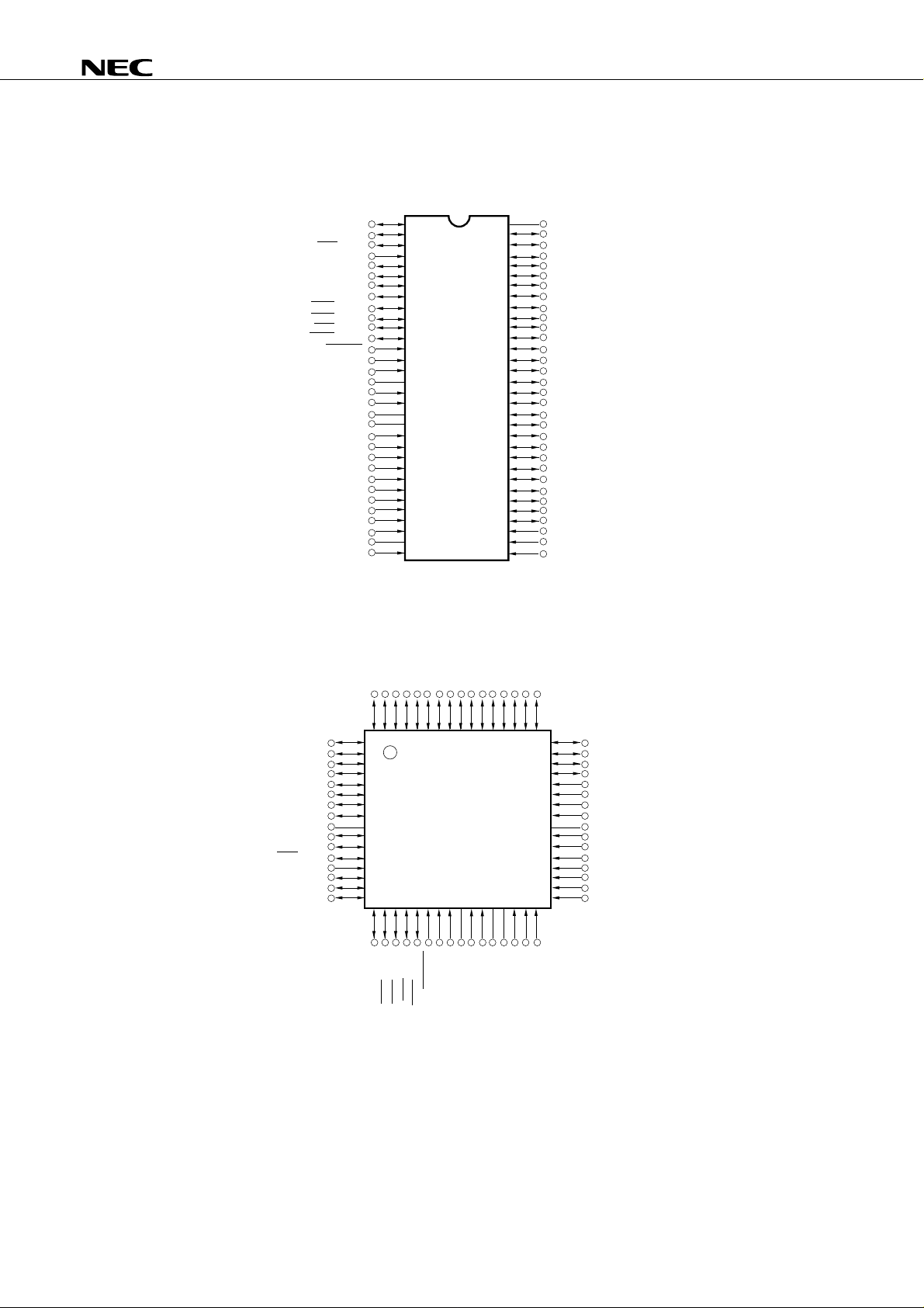
PIN CONFIGURATIONS (Top View)
• 64-pin plastic shrink DIP (750 mils)
µ
PD75P036
SB1/SI/P03
SB0/SO/P02
SCK/P01
INT4/P00
BUZ/P23
PCL/P22
PPO/P21
PTO0/P20
MAT/P103
MAZ/P102
MAI/P101
MAR/P100
RESET
X1
X2
V
XT1
XT2
V
AV
AV
REF+
AV
REF-
AN7
AN6
AN5
AN4
AN3/P113
AN2/P112
AN1/P111
AN0/P110
AV
TIO/P13
PP
DD
DD
SS
1
2
3
4
5
6
7
8
9
10
11
12
13
14
15
16
17
18
19
20
21
22
23
24
25
26
27
28
29
30
31
32
µ
PD75P036CW
• 64-pin plastic QFP (14 x 14 mm)
• 64-pin ceramic WQFN
64
63
62
61
60
59
58
57
56
55
54
53
52
51
50
49
48
47
46
45
44
43
42
41
40
39
38
37
36
35
34
33
V
SS
P30/MD0
P31/MD1
P32/MD2
P33/MD3
P40
P41
P42
P43
P50
P51
P52
P53
P60/KR0
P61/KR1
P62/KR2
P63/KR3
P70/KR4
P71/KR5
P72/KR6
P73/KR7
P80
P81
P82
P83
P90
P91
P92
P93
P10/INT0
P11/INT1
P12/INT2
P43
P42
P41
P40
MD3/P33
MD2/P32
MD1/P31
MD0/P30
V
SB1/SI/P03
SB0/SO/P02
SCK/P01
INT4/P00
BUZ/P23
PCL/P22
PPO/P21
P50
P51
P52
P53
P60/KR0
P61/KR1
P62/KR2
1
2
3
4
5
6
7
8
SS
9
10
11
12
13
14
15
16
171819
µ
PD75P036KG
X1
RESET
MAI/P101
PTO0/P20
MAT/P103
MAZ/P102
MAR/P100
P73/KR7
P80
P81
P72/KR6
52535455565758596061626364
51 50 49
DDAVDD
V
XT2
REF+
AV
P82
32313029282726252423222120
REF-
AV
48
47
46
45
44
43
42
41
40
39
38
37
36
35
34
33
P70/KR4
P63/KR3
P71/KR5
µ
PD75P036GC-AB8
PP
X2
V
XT1
P83
AN7
P90
P91
P92
P93
P10/INT0
P11/INT1
P12/INT2
TI0/P13
SS
AV
AN0/P110
AN1/P111
AN2/P112
AN3/P113
AN4
AN5
AN6
2

µ
PD75P036
PIN IDENTIFICATION
P00-P03 : Port 0 INT0, INT1, INT4: External Vectored Interrupt
P10-P13 : Port 1 INT2 : External Test Input
P20-P23 : Port 2 X1, X2 : Main System Clock Oscillation
P30-P33 : Port 3 XT1, XT2 : Subsystem Clock Oscillation
P40-P43 : Port 4 MAR : Reference Integration
P50-P53 : Port 5 Control
P60-P63 : Port 6 MAI : Integration Control
P70-P73 : Port 7 MAZ : Autozero Control
P80-P83 : Port 8 MAT : External Comparate
P90-P93 : Port 9 Timing Input
P100-P103 : Port 10 PPO : Programmable Pulse Output
P110-P113 : Port 11 ··· MFT timer mode
KR0-KR7 : Key Return AN0-AN7 : Analog Input
SCK : Serial Clock AV
SI : Serial Input AB
SO : Serial Output AV
REF+ : Analog Reference (+)
REF– : Analog Reference (–)
DD : Analog VDD
SB0, SB1 : Serial Bus AVSS : Analog VSS
RESET : Reset Input VDD : Positive Power Supply
TI0 : Timer Input V
SS : Ground
PTO0 : Programmable Timer Output MD0-MD3 : Mode Selection
BUZ : Buzzer Clock VPP : Programming/Verifying Power Supply
PCL : Programmable Clock
MFT A/D mode
★
Remark MFT: Multifunction Timer
3
4
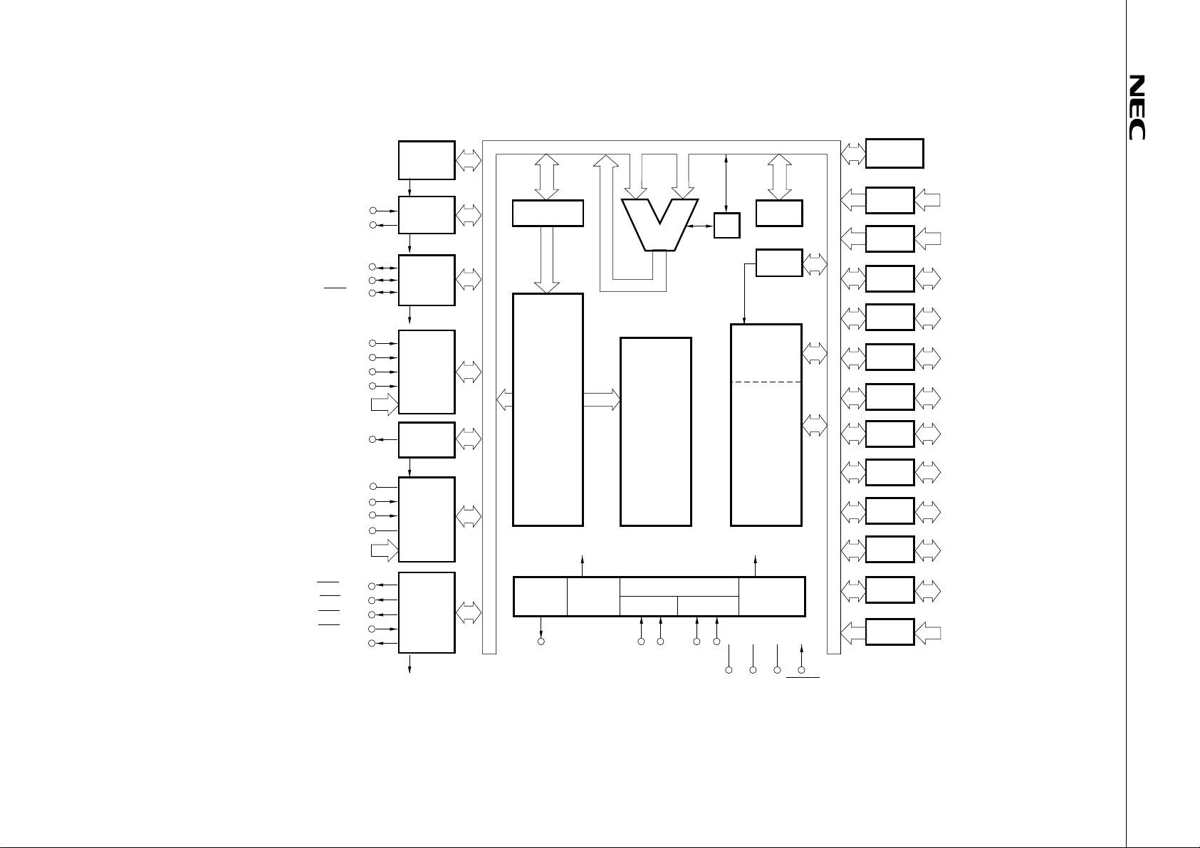
BLOCK DIAGRAM
TI0/P13
PTO0/P20
SI/SB1/P03
SO/SB0/P02
SCK/P01
INT0/P10
INT1/P11
INT2/P12
INT4/P00
KR0-KR3/P60-P63
KR4-KR7/P70-P73
BUZ/P23
AV
AV
REF+
AV
REF–
AV
AN0-AN3/P110-P113
AN4-AN7
MAR/P100
MAI/P101
MAZ/P102
MAT/P103
PPO/P21
BASIC
INTERVAL
TIMER
INTBT
TIMER
/COUNTER
#0
INTT0
SERIAL
INTERFACE
INTCSI
INTERRUPT
CONTROL
WATCH
TIMER
INTW
DD
A/D
CON-
SS
VERTER
MULTIFUNCTION
TIMER
INTMFT
PROGRAM
COUNTER
PROM
PROGRAM
MEMORY
16256 x 4 BITS
CLOCK
OUTPUT
CONTROL
PCL/P22
fx/2
CLOCK
DIVIDER
ALU
DECODE
AND
CONTROL
N
CLOCK GENERATOR
SUB
XT1 XT2 X1 X2
MAIN
CY
GENERAL
REG.
RAM
DATA
MEMORY
1024 x 4 BITS
STAND BY
CONTROL
V
PPVDDVSS
SP
BANK
CPU CLOCK
Φ
RESET
BIT SEQ.
BUFFER
PORT 0
PORT 1
PORT 2
PORT 3
PORT 4
PORT 5
PORT 6
PORT 7
PORT 8
PORT 9
PORT 10
PORT 11
P00–P03
P10–P13
P20–P23
P30/MD0-P33/MD3
P40–P43
P50–P53
P60–P63
P70–P73
P80–P83
P90–P93
P100–P103
P110–P113
µ
PD75P036

CONTENTS
1. PIN FUNCTIONS ... 6
1.1 Port Pins ... 6
1.2 Non-Port Pins ... 8
1.3 Pin Input/Output Circuits ... 10
1.4 Recommended Connection of Unused Pins ... 13
2. MEMORY ... 14
2.1 Differences between µPD75P036 and µPD75028/75036 ... 14
2.2 Program Memory (ROM) ... 15
2.3 Data Memory (RAM) ... 17
3. WRITING AND VERIFYING PROM (PROGRAM MEMORY) ... 19
3.1 Operation Modes For Writing/Verifying Program Memory ... 19
3.2 Program Memory Write Procedure ... 20
3.3 Program Memory Read Procedure ... 21
3.4 Erasure (µPD75P036KG only) ... 22
µ
PD75P036
★
★
4. ELECTRICAL SPECIFICATIONS ... 23
5. CHARACTERISTIC CURVES ... 38
6. PACKAGE DRAWINGS ... 44
7. RECOMMENDED SOLDERING CONDITIONS ... 47
APPENDIX A. DEVELOPMENT TOOLS ... 48
APPENDIX B. RELATED DOCUMENTS ... 49
★
★
5
µ
PD75P036
1. PIN FUNCTIONS
1.1 Port Pins (1/2)
Pin Name Input/Output Alternate Function 8-Bit I/O When Reset Input/Output
Function Circuit
P00 Input INT4 4-bit input port (PORT0). No Input B
P01 Input/Output SCK Internal pull-up resistors can be specified in F - A
P02 Input/Output SO/SB0 3-bit units for the P01 to P03 pins by F - B
P03 Input/Output SI/SBI software. M - C
P10 Input INT0 With noise elimination function No Input B - C
P11 INT1 4-bit input port (PORT1).
P12 INT2 Internal pull-up resistors can be specified in
P13 TI0 4-bit units by software.
P20 Input/Output PTO0 4-bit input/output port (PORT2). No Input E - B
P21 PPO Internal pull-up resistors can be specified in
P22 PCL 4-bit units by software.
P23 BUZ
Note 2
P30
P31
P32
P33
Input/Output MD0 Programmable 4-bit input/output port No Input E - B
Note 2
Note 2
Note 2
MD1 (PORT3).
MD2 This port can be specified for input/output
MD3 in bit units.
Internal pull-up resistors can be specified in
4-bit units by software.
Note 2
N-ch open-drain 4-bit input/output port Yes Input M - A
P40-P43 Input/Output (PORT4).
Withstands up to 10 V.
Data input/output pin for writing and verifying
of program memory (PROM) (lower 4 bits).
Note 2
Input/Output N-ch open-drain 4-bit input/output port Input M - A
P50-P53 (PORT5).
Withstands up to 10 V.
Data input/output pin for writing and verifying
of program memory (PROM) (upper 4 bits).
Type
Note 1
Notes 1. Circles indicate Schmitt-triggerred inputs.
2. Can directly drive LEDs.
6
µ
PD75P036
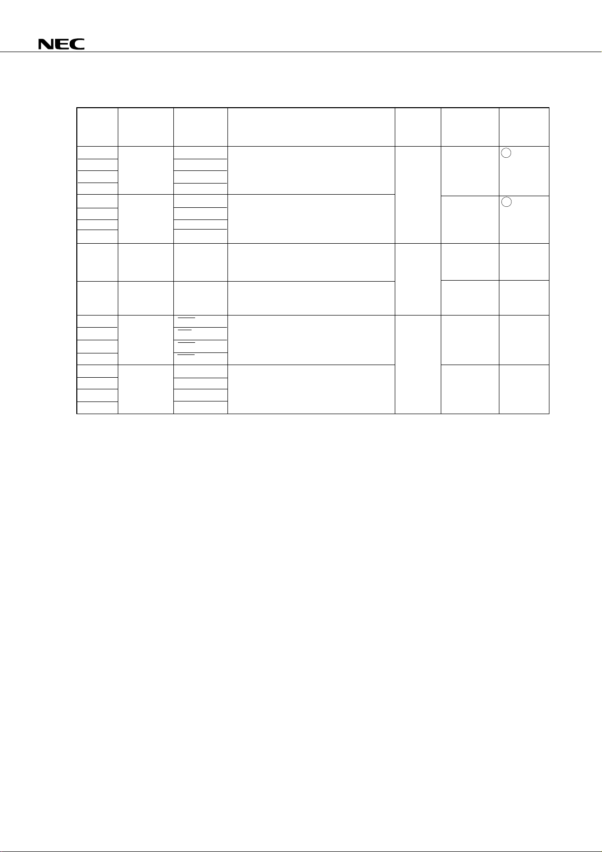
1.1 Port Pins (2/2)
Pin Name Input/Output Alternate Function 8-Bit I/O When Reset Input/Output
Function Circuit
P60 Input/Output KR0 Programmable 4-bit input/output port Yes Input F - A
P61 KR1 (PORT6).
P62 KR2 Internal pull-up resistors can be specified in
P63 KR3 4-bit units by software.
P70 Input/Output KR4 4-bit input/output port (PORT7). Input F - A
P71 KR5 Internal pull-up resistors can be specified in
P72 KR6 4-bit units by software.
P73 KR7
P80-P83 Input/Output — 4-bit input/output port (PORT8). No Input E - B
Internal pull-up resistors can be specified in
4-bit units by software.
P90-P93 Input/Output — 4-bit input/output port (PORT9). Input E - D
Internal pull-up resistors can be specified in
4-bit units by software.
P100 Input/Output MAR N-ch open-drain 4-bit input/output port No Input M -A
P101 MAI (PORT10).
P102 MAZ Withstands up to 10 V in open-drain mode.
P103 MAT
P110 Input AN0 4-bit input/output port (PORT11). Input Y
P111 AN1
P112 AN2
P113 AN3
Type
Note 1
Note Circles indicate schmitt-triggerred inputs.
7
µ
PD75P036
1.2 Non-Port Pins (1/2)
Pin Name Input/Output Alternate Function 8-Bit I/O When Reset Input/Output
Function Circuit
TI0 Input P13 External event pulse input pin to timer/event counter Input B - C
PTO0 Input/Output P20 Timer/event counter output pin Input E - B
PCL Input/Output P22 Clock output pin Input E - B
BUZ Input/Output P23 Fixed frequency output pin (for buzzer or for trimming Input E - B
the system clock)
SCK Input/Output P01 Serial clock input/output pin Input F - A
SO/SB0 Input/Output P02 Serial data output pin Input F - B
Serial bus input/output pin
SI/SB1 Input/Output P03 Serial data output pin Input M - C
Serial bus input/output pin
INT4 Input P00 Edge detection vectored interrupt input pin (Either Input B
rising or falling edge detection is effective)
INT0 Input P10 Edge detection vectored interrupt input pin (Detection Input B - C
INT1 P11 edge can be selected)
INT2 Input P12 Edge detection testable input pin (rising edge detection) Input B - C
KR0-KR3 Input/Output P60-P63 Testable input/output pin (parallel falling edge detection) Input F - A
KR4-KR7 Input/Output P70-P73 Testable input/output pin (parallel falling edge detection) Input F - A
MAR Input/Output P100 In integral A/D Reverse integration signal output pin Input M - A
MAI Input/Output P101 converter mode Integration signal output pin Input M - A
MAZ Input/Output P102 of MFT Auto zero signal output pin Input M - A
MAT Input/Output P103 Comparator input pin Input M - A
PPO Input/Output P21 In timer mode Timer pulse output pin Input E - B
of MFT
Type
Note 1
Note Circles indicate Schmitt-triggerred inputs.
Remark MFT: Multifunction timer
8
µ
PD75P036
1.2 Non-Port Pins (2/2)
Pin Name Input/Output Alternate Function When Reset Input/Output
Function Circuit
AN0-AN3 Input P110-P113 Pins only for A/D 8-bit analog input pin. — Y
AN4-AN7 — converter Y - A
AVREF+ Input — Reference voltage input — Z - A
pin (AVDD side).
AVREF– Input — Reference voltage input — Z - A
pin (AVSS side).
AVDD — — Positive power supply pin. — —
AVSS — — GND potential pin. — —
X1, X2 Input — Crystal or ceramic resonator connection for main — —
system clock generation. To use external clock, input
the external clock to X1 and its reverse phase to X2.
XT1, XT2 Input — Crystal or ceramic resonator connection for subsystem — —
clock generation. To use external clock, input the
external clock to XT1 and its reverse phase to XT2.
XT1 can be used as a 1-bit input (test) pin.
RESET Input — System reset input pin. — B
MD0/MD3 Input/Output P30-P33 Mode selection pins in program memory (PROM) Input E - B
Note 2
VPP
VDD — — Positive power supply pin. — —
VSS — — GND potential pin. — —
— — Program voltage application pin in program memory — —
write/verify mode.
(PROM) write/verify mode.
At normal operation, connect the pin to VDD directly.
In the PROM write/verify mode, apply +12.5 V.
Type
Note 1
Notes 1. Circles indicate schmitt trigger inputs.
2. If the V
PP pin is not connected directly to the VDD pin at normal operation, the
normally.
µ
PD75P036 does not operate
9
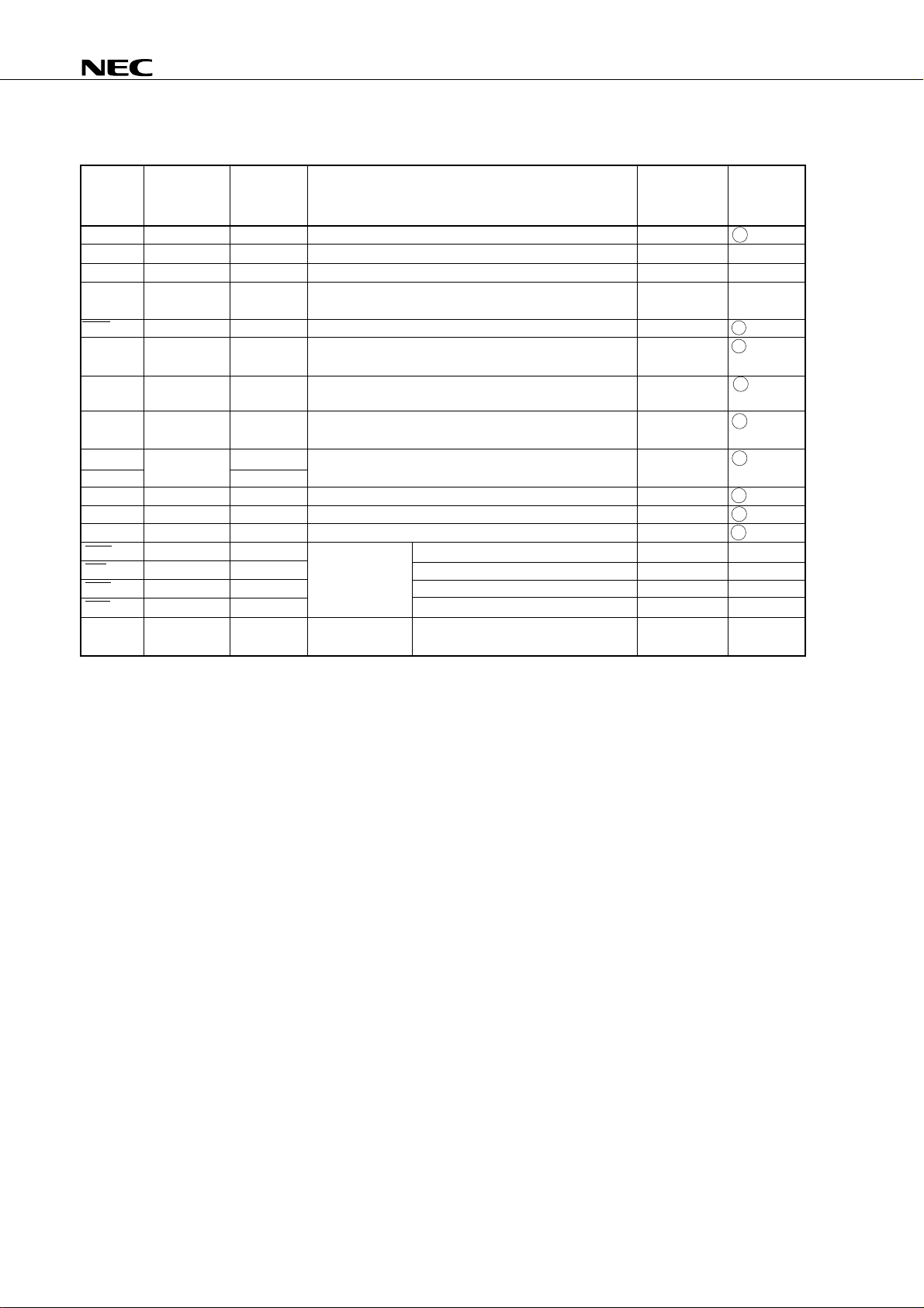
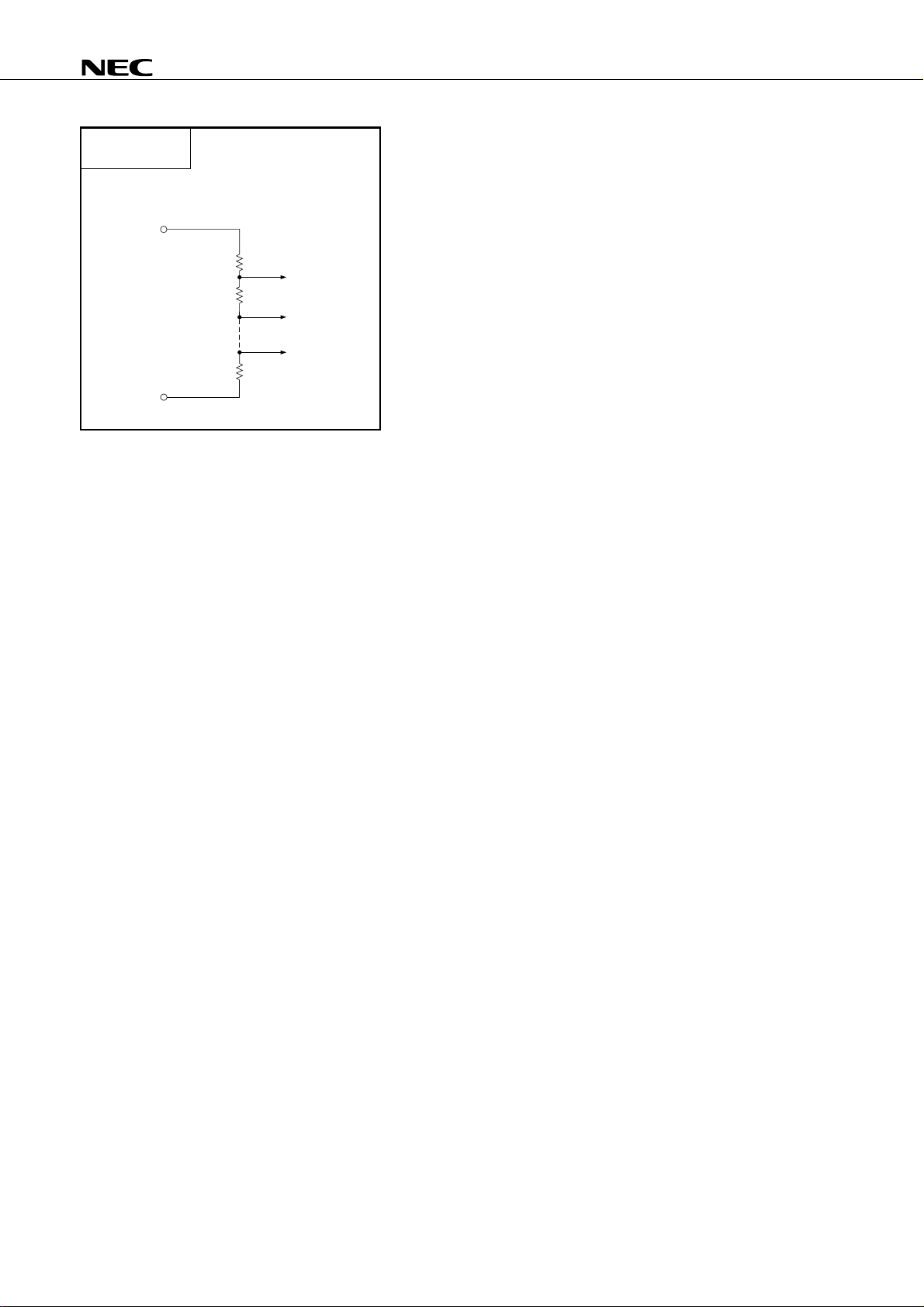
1.3 Pin Input/Output Circuits
The following shows a simplified input/output circuit diagram for each pin of the
µ
PD75P036.
µ
PD75P036
TYPE A (for TYPE E - B)
V
DD
P-ch
IN
N-ch
CMOS-level input buffer
TYPE B
IN
Schmitt-triggerred input with hysteresis characteristics
TYPE D (for TYPE E - B, F - A)
V
DD
data
output
disable
Push-pull output that can be set in an output
high-impedance state (both P-ch and N-ch are off)
TYPE E - B
P.U.R.
enable
data
output
disable
P.U.R. : Pull-Up Resistor
Type D
Type A
P-ch
N-ch
V
DD
OUT
P.U.R.
P-ch
IN/OUT
10
TYPE B - C
P-ch
IN
V
DD
P.U.R.
P.U.R.
enable
P.U.R. : Pull-Up Resistor
TYPE E - D
data
output
disable
P.D.R. : Pull-Down Resistor
Type D
Type A
P.D.R.
enable
IN/OUT
N-ch
P.D.R.
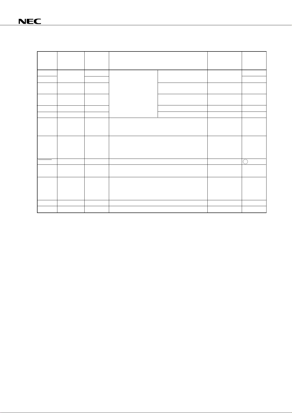
µ
PD75P036
TYPE F - A
output
disable
TYPE F - B
output
disable
(P)
data
output
disable
P.U.R.
enable
data
P.U.R. : Pull-Up Resistor
output
disable
(N)
Type D
P.U.R.
enable
Type B
TYPE M - C
V
DD
P.U.R. P.U.R.
P-ch P-ch
IN/OUT
data
P.U.R.
enable
N-ch
output
disable
P.U.R. : PullUp Resistor
TYPE Y
V
DD
P.U.R.
V
DD
P-ch
N-ch
P-ch
IN/OUT
IN
AV
P-ch
N-ch
DD
Sam-
pling
C
AV
SS
Reference voltage
(from serial resistor
input
string voltage tap)
enable
V
+
–
DD
AV
AV
IN/OUT
DD
SS
TYPE M - A
data
output
disable
P.U.R. : Pull-Up Resistor
N-ch
(+10-V
voltage)
Middle-voltage input buffer
(withstands up to + 10 V)
P.U.R. : Pull-Up Resistor
IN/OUT
TYPE Y - A
IN
AV
DD
P-ch
N-ch
AV
IN instruction
Input buffer
AV
DD
+
Sam-
pling
–
C
AV
SS
SS
Reference voltage
(from serial resistor
string voltage tap)
11
TYPE Z - A
AVREF+
AVREF-
Reference voltage
µ
PD75P036
12
µ
PD75P036
1.4 Recommended Connection of Unused Pins
Pin Name Recomended Connecting Method
P00/INT4 Connect to VSS.
P01/SCK Connect to VSS or VDD.
P02/SO/SB0
P03/SI/SB1
P10/INT0-P12/INT2 Connect to VSS.
P13/TI0
P20/PTO0 Input state: Independently connect to VSS or VDD via a
P21/PPO resistor.
P22/PCL Output state: Leave Open.
P23/BUZ
P30/MD0-P33/MD3
P40-P43
P50-P53
P60/KR0-P63/KR3
P70/KR4-P73/KR7
P80-P83
P90-P93
P100/MAR
P101/MAI
P102/MAZ
P103/MAT
P110/AN0-P113/AN3 Connect to VSS or VDD.
AN4-AN7
AVREF+ Connect to VSS.
AVREF–
AVSS
AVDD Connect to VDD.
XT1 Connect to VSS or VDD.
XT2 Leave Open.
VPP Connect directly to VDD.
★
13
µ
PD75P036
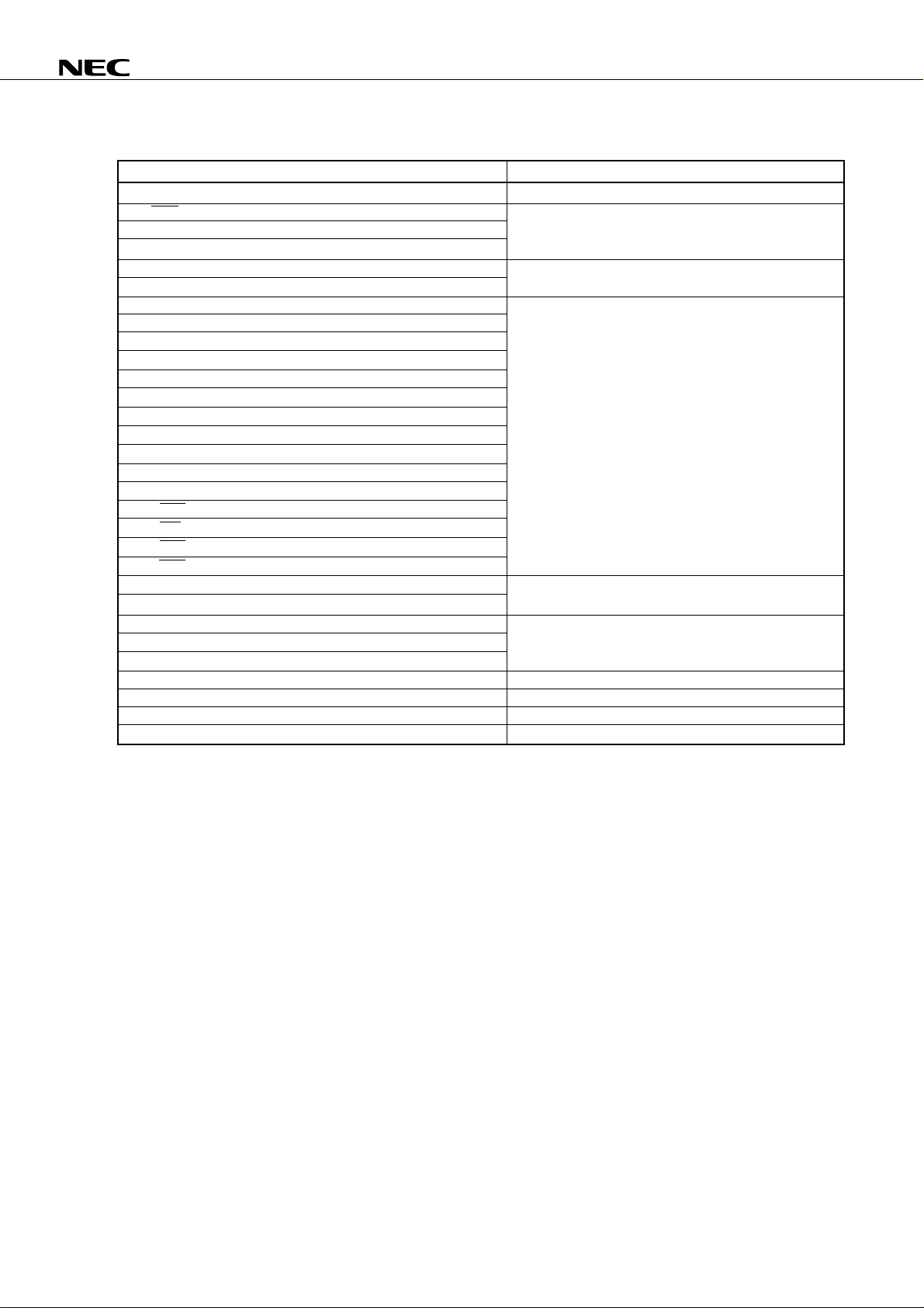
2. MEMORY
2.1 Differences between µPD75P036 and µPD75028/75036
µ
PD75P036 is a microcontroller provided by replacing the µPD75028's on-chip mask ROM with one-time
The
PROM or EPROM. Capacity of program memory and data memory are different, but CPU function and internal
hardware are identical. Table 2-1 shows the differences between the µPD75P036 and µPD75028/75036. Users
should fully consider these differences especially when debugging or producing an application system on an
experimental basis by using the PROM version and then mass-producing the system using the mask ROM version.
µ
For details about the CPU function and the internal hardware, refer to
PD75028 User's Manual (IEM-1280).
★
Item
Program memory One-time PROM/EPROM Mask ROM
Data memory 000H-3FFH 000H-1FFH 000H-3FFH
Pull-up resistor Ports 0-3, 6-8 Can be specified by software.
Pull-down resistor Port 9 Can be specified by software.
XT1 feedback resistor Provided on-chip Can be disconnected by mask option
Supply voltage VDD = 2.7 to 6.0 V
Pin connection Pin 16 (SDIP) VPP Internally connected
Electrical specifications Supply current and operating temperature ranges differ between µPD75P036 and
Others Noise immunity and noise radiation differ because circuit complexity and mask layout are
Table 2-1. Differences between µPD75P036 and µPD75028/75036
µ
PD75P036
0000H-3F7FH 0000H-1F7FH 0000H-3F7FH
(16256 x 8 bits) (8064 x 8 bits) (16256 x 8 bits)
(1024 x 4 bits) (512 x 4 bits) (1024 x 4 bits)
Ports 4, 5, 10 Not provided Can be connected by mask option
Pin 25 (QFP)
Pins 60-63 P33/MD3-P30/MD0 P33-P30
(SDIP)
Pins 5-8 (QFP)
µ
PD75028/75036. For details, refer to the electrical specifications described in Data Sheet
of each model.
different.
µ
PD75028
µ
PD75036
Caution The noise immunity and noise radiation differ between the PROM and mask ROM versions. To
replace the PROM version with the mask ROM version in the course of experimental production
to mass production, evaluate your system by using the CS version (not ES) of the mask ROM
version.
14

µ
PD75P036
2.2 Program Memory (ROM) ··· 16256 words x 8 bits
The program memory is a 16256-word x 8-bit PROM and stores programs, table data, etc.
The program memory is accessed by referencing the program counter contents. Table data can be referenced
by executing a table look-up instruction (MOVT).
Figure 2-1 shows the address range in which a branch can be taken by branch instructions and subroutine call
instructions. A relative branch instruction (BR $addr) enables a branch to addresses [PC value –15 to –1, +2 to
+16] regardless of block boundaries.
Program memory addresses are 0000H-3F7FH and the following addresses are assigned to special purposes:
(All areas except 0000H or 0001H can be used as normal program memory.)
• Addresses 0000H-0001H
Vector table into which the program start address and MBE setting value when the RESET signal is generated
are written.
Processing at reset is started at any desired address.
• Addresses 0002H-000DH
Vector table into which the program start address and MBE setting value when each vectored interrupt is
generated are written.
Interrupt servicing can be started at any desired address.
• Addresses 0020H-007FH
Table area referenced by the GETI instruction
Note
.
Note The GETI instruction is provided to execute any 2-byte or 3-byte instruction or two 1-byte instructions as a 1-
byte instruction; it is used to reduce the number of program steps.
15
µ
PD75P036
Address
0000H
0002H
0004H
0006H
0008H
000AH
000CH
7
MBE
MBE
MBE
MBE
MBE
MBE
MBE
Figure 2-1. Program Memory Map
6
0
Internal reset start address (high-order six bits)
Internal reset start address (low-order eight bits)
INTBT/INT4 start address (high-order six bits)
0
INTBT/INT4 start address (low-order eight bits)
INT0 start address (high-order six bits)
0
INT0 start address (low-order eight bits)
INT1 start address (high-order six bits)
0
INT1 start address (low-order eight bits)
INTCSI start address (high-order six bits)
0
INTCSI start address (low-order eight bits)
INT0 start address (high-order six bits)
0
INT0 start address (low-order eight bits)
INTMFT start address (high-order six bits)
0
INTMFT start address (low-order eight bits)
0
CALLF
! faddr
instruction
address
entry
BRCB
! caddr
instruction
branch
address
CALL ! addr
instruction
subroutine
entry addres
BR ! addr
Instruction
branch
address
BR $ addr
instruction
relative
branch Address
(–15 to –1 and
+2 to +16)
0020H
007FH
0080H
07FFH
0800H
0FFFH
1000H
1FFFH
2000H
2FFFH
3000H
3F7FH
GETI instruction reference table
BRCB ! caddr
instruction
branch addresses
BRCB ! caddr
instruction
branch addresses
BRCB ! caddr
instruction
branch addresses
Branch destination
address and
subroutine entry
address to be set
by GETI instruction
16

µ
PD75P036
2.3 Data Memory (RAM)
The data memory consists of a data area and a peripheral hardware area as shown in Figure 2-2.
The data memory consists of banks, each consisting of 256 words x 4 bits, and the following memory banks can
be used:
• Memory banks 0-3 (data area)
• Memory bank 15 (peripheral hardware area)
Figure 2-2. Data Memory Map
Data Memory Memory Bank
General purpose
register area
Stack area
000H
007H
008H
0FFH
100H
(8 x 4)
256 x 4
256 x 4
0
1
Data area
Static RAM
(1024 x 4)
Peripheral
hardware area
1FFH
200H
2FFH
300H
3FFH
F80H
FFFH
256 x 4
256 x 4
Not implemented
128 x 4
2
3
15
17

µ
(1) Data area
The data area consists of static RAM and is used to store process data and as stack memory when a
(subroutine) or an interrupt is executed. Even when CPU operation is stopped in the standby mode, the memory
contents can be retained for hours with battery backup, etc. The data area is manipulated by executing memory
manipulation instructions.
The static RAM is mapped each 256 x 4 bits in memory banks 0-3. Bank 0 is mapped as a data area; it can
also be used as a general purpose register area (000H-007H) and a stack area (000H-0FFH).
One address of the static RAM consists of four bits; however it can be manipulated in 8-bit units by executing
8-bit memory manipulation instructions and bit-wise by executing bit manipulation instructions. To execute an
8-bit memory manipulation instruction, specify an even address.
(a) General purpose register area
Can be handled by executing general purpose register and memory manipulation instructions. A maximum
of eight 4-bit registers can be used. The portions of the eight general purpose registers not used by a
program can be used as a data area or stack area.
(b) Stack area
Is set by an instruction and can be used as a save area when a subroutine is executed or interrupt servicing
is performed.
PD75P036
(2) Peripheral hardware area
The peripheral hardware area is mapped in addresses F80H-FFFH of memory bank 15.
Like the static memory, the peripheral hardware area is handled by executing memory manipulation instructions.
However, the bit units in which the peripheral hardware can be manipulated vary depending on the address.
Addresses in which the peripheral hardware is not mapped do not contain data memory and cannot be
accessed.
18

µ
PD75P036
3. WRITING AND VERIFYING PROM (PROGRAM MEMORY)
The program memory incorporated in the µPD75P036 is a 16256 x 8-bit electrically writable PROM. The pins
as listed in the table given below are used for write and verification of the PROM. No address is input; instead, an
address is updated by inputting a clock from the X1 pin.
Pin Name Function
VPP Applies voltage when program memory is written/verified (normally, at VDD potential)
X1, X2 These pins input clock that updates address when program memory is written/verified. To X2 pin,
input X1's signal reverse phase.
MD0-MD3 (P30-P33) These pins select operation mode when program memory is written/verified.
P40-P43 (Lower 4) These pins input/output 8-bit data when program memory is written/verified.
P50-P53 (Upper 4)
VDD Power supply voltage application pin.
Apply 2.7 to 6.0 V to this pin during normal operation and 6 V when program memory is written/verified.
Cautions 1. Always cover the erasure window of the µPD75P036KG with an opaque film except when the
contents of the EPROM are erased.
2. The one-time PROM version µPD75P036CW/GC is not equipped with a window, and therefore,
the contents of the program memory of this model cannot be erased by exposing it to ultraviolet
rays.
3.1 Operation Modes For Writing/Verifying Program Memory
When +6V is applied to the V
DD pin of the
µ
PD75P036 with +12.5V applied to the VPP pin, the µPD75P036 is set
in the program memory write/verify mode. In this mode, the following operation modes can be set by using the MD0-
SS
MD3 pins. At this time, all remaining pins are set to the V
Operating Mode Specification Operating Mode
VPP VDD MD0 MD1 MD2 MD3
+12.5 V +6 V H L H L Program memory address 0 clear mode
L H H H Write mode
L L H H Verify mode
H X H H Program inhibit mode
potential with pull-down resistors.
x: L or H
★
19

3.2 Program Memory Write Procedure
The program memory write procedure is as follows. High-speed program memory write is possible.
µ
PD75P036
(1) Connect the unused pins to V
(2) Supply 5 V to the V
(3) Wait for 10
µ
DD and VPP pins.
s.
SS via pull-down resistors. The X1 pin must be low.
(4) Set program memory address 0 clear mode.
(5) Supply 6 V to the VDD pin and 12.5 V to the VPP pin.
(6) Set program inhibit mode.
(7) Write data in 1 ms write mode.
(8) Set program inhibit mode.
(9) Set verify mode. If data has been written connectly, proceed to step (10). If data has not yet been written,
repeat steps (7) to (9).
(10) Write additional data for (the number of times data was written (X) in steps (7) to (9)) times
1 ms.
(11) Set program inhibit mode.
(12) Supply a pulse to the X1 pin four times to update the program memory address by 1.
(13) Repeat steps (7) to (12) to the last address.
(14) Set program memory address 0 clear mode.
(15) Change the voltages of V
DD and VPP pins to 5 V.
(16) Turn off the power supply.
Steps (2) to (12) are illustrated below.
V
V
PP
V
VDD+1
V
DD
V
X1
P40-P43
P50-P53
MD0
(P30)
MD1
(P31)
MD2
(P32)
MD3
(P33)
X-time repetition
Write Verify
PP
DD
DD
Data input
Data
output
Additional
data write
Data input
Address
increment
20

3.3 Program Memory Read Procedure
µ
PD 75P036 program memory contents can be read in the following procedure. Read operation should be
The
performed in the verify mode.
µ
PD75P036
(1) Connect the unused pins to V
(2) Supply 5 V to the V
(3) Wait for 10
µ
DD and VPP pins.
s.
SS via pull-down resistors. The X1 pin must be low.
(4) Set program memory address 0 clear mode.
(5) Supply 6 V to the V
DD pin and 12.5 V to the VPP pin.
(6) Set program inhibit mode.
(7) Set verify mode. Data of each address is sequentially output each time a clock pulse is input to the X1 pin
four times.
(8) Set program inhibit mode.
(9) Set program memory address 0 clear mode.
(10) Change the voltages of V
DD and VPP pins to 5 V.
(11) Turn off the power supply.
Steps (2) to (9) are illustrated below.
V
PP
V
PP
V
DD
VDD+1
V
DD
V
DD
X1
P40-P43
P50-P53
MD0
(P30)
MD1
(P31)
MD2
(P32)
MD3
(P33)
"L"
Data output
Data output
21

★
3.4 Erasure (µPD75P036KG only)
The contents of the data programmed to the
rays.
The wavelength of the ultraviolet rays used to erase the contents is about 250 nm, and the quantity of the
ultraviolet rays necessary for complete erasure is 15 W•s/cm
When a commercially available ultraviolet ray lamp (wavelength: 254 nm, intensity: 12 mW/cm
15 to 20 minutes is required.
Cautions 1. The contents of the program memory may be erased if the
time to direct sunlight or a fluorescent light. To protect the contents from being erased, mask
the window with the opaque film. NEC attaches quality-tested opaque film to the UV EPROM
products for shipping.
2. To erase the memory contents, the distance between the ultraviolet ray lamp and the
should be 2.5 cm or less.
Remark The time required for erasure changes depending on the degradation of the ultraviolet ray lamp and the
surface condition (dirt) of the window.
µ
PD75P036 can be erased by exposing the window to ultraviolet
2
(= ultraviolet ray intensity x erasure time).
2
) is used, about
µ
PD75P036 is exposed for a long
µ
PD75P036
µ
PD75P036
22

µ
PD75P036
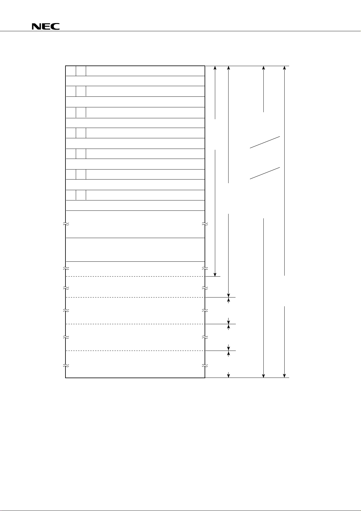
4. ELECTRICAL SPECIFICATIONS
Absolute Maximum Ratings (TA = 25 °C)
Parameter Symbol Test Conditions Ratings Unit
Supply voltage VDD –0.3 to +7.0 V
VPP –0.3 to +13.5 V
Input voltage VI1 Other than ports 4, 5, or 10 –0.3 to VDD+0.3 V
VI2 Ports 4, 5 and 10 Open-drain –0.3 to +11 V
Output voltage VO –0.3 to VDD+0.3 V
Output current, high IOH Per pin –10 mA
All pins –30 mA
Output current, low IOL
Operating ambient temperature TA –40 to +70 °C
Storage temperature Tstg –65 to +150 °C
Note
Ports 0, 3, 4 and 5 peak value 30 mA
Per pin r.m.s. value 15 mA
Other than ports peak value 20 mA
0, 3, 4 and 5 r.m.s. value 5 mA
Per pin
Total for ports 0, 3-9, 11 peak value 170 mA
r.m.s. value 120 mA
Total for 0, 2, 10 peak value 30 mA
r.m.s. value 20 mA
★
Note r.m.s. values should be calculated as follows: [r.m.s. value] = [peak value] x Duty
Caution Product quality may suffer if the absolute maximum rating is exceeded for even a single parameter,
or even momentarily. In other words, the absolute maximum ratings are rated values at which the
product is on the verge of suffering physical damage, and therefore the product must be used under
conditions which ensure that the absolute maximum ratings are not exceeded.
Capacitance (TA = 25 °C, VDD = 0 V)
Parameter Symbol Test Conditions MIN. TYP. MAX. Unit
Input capacitance C I f = 1 MHz 15 pF
Output capacitance CO Unmeasured pins returned to 0 V 15 pF
I/O capacitance CIO 15 pF
★
23

µ
PD75P036
Main System Clock Oscillator Characteristics (TA = –40 to +70 °C, VDD = 2.7 to 6.0 V)
Resonator Recommended Parameter Test Conditions MIN. TYP. MAX. Unit
Constants
Ceramic Oscillation frequency VDD = Oscillation voltage 2.0 5.0
resonator (fX)
X1 X2
Note 1
range
Oscillation stabilization After VDD came to MIN. 4 ms
C1 C2
V
DD
time
of oscillation voltage range
Note 2
Crystal Oscilaltion frequency 2.0 4.19 5.0
resonator (fX)
X1 X2
Note 1
Oscillation stabilization VDD = 4.5 to 6.0 V 10 ms
Note 2
C1 C2
V
time
DD
External clock X1 input frequency 2.0 5.0
X1 X2
(fX)
Note 1
X1 input high- and 100 250 ns
PD74HCU04
µ
low-level widths (tXH, tXL)
Note 3
Note 3
30 ms
Note 3
MHz
MHz
MHz
Notes 1. The oscillation frequency and X1 input frequency are indicated only to express the characteristics of the
oscillator. For instruction execution time, refer to AC Characteristics.
2. Time required for oscillation to stabilize after V
reaches the minimum value of the oscillation voltage
DD
range or the STOP mode has been released.
3. When the oscillation frequency is 4.19 MHz < fx ≤ 5.0 MHz, do not select PCC = 0011 as the instruction
µ
execution time: otherwise, one machine cycle is set to less than 0.95
value of 0.95
★
Caution When using the oscillation circuit of the main system clock, wire the portion enclosed in dotted
µ
s.
s, falling short of the rated minimum
line in the figures as follows to avoid adverse influences on the wiring capacity:
• Keep the wiring length as short as possible.
• Do not cross the wiring over the other signal lines. Do not route the wiring in the vicinity of
lines through which a high alternating current flows.
• Always keep the ground point of the capacitor of the oscillator circuit at the same potential as
DD. Do not connect the power source pattern through which a high current flows.
V
• Do not extract signals from the oscillation circuit.
24

µ
PD75P036
Subsystem Clock Oscillator Characteristics (TA = –40 to +70 °C, VDD = 2.7 to 6.0 V)
Resonator Recommended Parameter Test Conditions MIN. TYP. MAX. Unit
Constants
Crystal Oscillation frequency 32 32.768 35 kHz
resonator (fX)
External clock X1 input frequency 32 100 kHz
XT1 XT2
R
C3 C4
V
DD
X1 X2
Notes 1. The oscillation frequency and XT1 input frequency are indicated only to express the characteristics of
the oscillator. For instruction execution time, refer to AC Characteristics.
2. Time required for oscillation to stabilize after VDD reaches the minimum value of the oscillation voltage
range.
Note 1
Oscillation stabilization VDD = 4.5 to 6.0 V 1.0 2 s
Note 2
time
10 s
Note 1
(fX)
X1 input high-, low-level 5 15
widths (tXH, tXL)
µ
s
Cautions When using the oscillation circuit of the main system clock, wire the portion enclosed in dotted
line in the figures as follows to avoid adverse influences on the wiring capacity:
• Keep the wiring length as short as possible.
• Do not cross the wiring over the other signal lines. Do not route the wiring in the vicinity of lines
through which a high alternating current flows.
• Always keep the ground point of the capacitor of the oscillator circuit at the same potential as
DD. Do not connect the power source pattern through which a high current flows.
V
• Do not extract signals from the oscillation circuit.
The amplification factor of the subsystem clock oscillation circuit is designed to be low to reduce the current
dissipation and therefore, the subsystem clock circuit is influenced by noise more easily than the main
system clock oscillation circuit. When using th subsystem clock, therefore, exercise utmost care in wiring
the circuit.
★
25

µ
PD75P036
DC Characteristics (TA = –40 to +70 °C, VDD = 2.7 to 6.0 V)
Parameter Symbol Test Conditions MIN. TYP. MAX. Unit
Input voltage, high VIH1 Ports 2, 3, 8, 9, 11 0.7VDD VDD V
VIH2 Ports 0, 1, 6, 7, RESET 0.8VDD VDD V
VIH3 Ports 4, 5, 10 Open-drain 0.7VDD 10 V
VIH4 X1, X2, XT1, XT2 VDD–0.5 VDD V
Input voltage, low VIL1 Ports 2 to 5, 8 to 11 0 0.3VDD V
VIL2 Ports 0, 1, 6, 7, RESET 0 0.2VDD V
VIL3 X1, X2, XT1, XT2 0 0.4 V
Output voltage, high VOH VDD = 4.5 to 6.0 V, IOH = –1 mA VDD–1.0 V
IOH = –100 µAVDD–0.5 V
Output voltage, low VOL Ports 3, 4, 5 VDD = 4.5 to 6.0 V, 0.4 2.0 V
IOL = 15 mA
VDD = 4.5 to 6.0 V, IOL = 1.6 mA 0.4 V
IOL = 400 µA 0.5 V
SB0, 1 Open-drain 0.2VDD V
Pull-up Resistor ≥ 1 kΩ
Input leakage current, high ILIH1 VI = VDD Other than below 3
ILIH2 X1, X2, XT1, XT2 20
ILIH3 VI = 9 V Ports 4, 5, 10 20
(Open-drain)
Input leakage current, low ILIL1 VI = 0 V Other than below –3
ILIL2 X1, X2, XT1, XT2 –20
Input leakage current, high ILOH1 VO = VDD 3
ILOH2 VO = 9 V Ports 4, 5, 10 20
(Open-drain)
Input leakage current, low ILOL VO = 0 V –3
Internal pull-up resistor RUI Ports 0, 1, 2, VDD = 5.0 V ± 10 %154080kΩ
3, 6, 7, 8 VDD = 3.0 V ± 10 % 30 300 kΩ
(except P00)
VI = VDD
Internal pull-down resistor RD Port 9 VDD =5.0 V ± 10 %104070kΩ
VI = VDD VDD = 3.0 V ± 10 % 10 60 kΩ
µ
µ
µ
µ
µ
µ
µ
µ
A
A
A
A
A
A
A
A
26

µ
PD75P036
Parameter Symbol Test Conditions MIN. TYP. MAX. Unit
Supply current
Note 1
IDD1 4.19 MHz VDD = 5 V ± 10%
Crystal VDD = 3 V ± 10%
IDD2 oscillator
C1 = C2 = 22 pF mode V DD = 3 V ± 10% 300 900
IDD3 32.768 kHz Operating VDD = 3 V ± 10% 100 300
Crystal mode
IDD4 oscillator
IDD5 XT1 = 0 V VDD = 5 V ± 10% 0.5 20
STOP mode V DD = 0.1 10
IDD6 32.768 kHz V DD = 3 V ± 10%
Crystal oscillator
STOP mode
Note 2
Note 5
HALT VDD = 5 V ± 10% 700 2100
HALT VDD = 3 V ± 10% 20 60
mode
3 V ± 10% TA = 25˚C 0.1 5
Note 3
Note 4
Note 6
4.5 14 mA
0.9 3 mA
515
Notes 1. Currents for the internal pull-up resistor are not included.
2. Including when the subsystem clock is operated.
3. High-speed mode operation (when processor clock control register (PCC) is set to 0011).
4. Low-speed mode operation (when PCC is set to 0000).
5. When operated with the subsystem clock by setting the system clock control register (SCC) to SCC3 =
1 and SCC0 = 0 to stop the main system clock operation.
6. When subsystem clock is operated by executing STOP instruction during main system clock operation.
µ
A
µ
A
µ
A
µ
A
µ
A
µ
A
µ
A
µ
A
27

AC CHARACTERISTICS (TA = –40 to +70 °C, VDD = 2.7 to 6.0 V)
µ
PD75P036
Parameter Symbol Conditions MIN. TYP. MAX. Unit
CPU clock cycle time
(minimum instruction execution main system clock 3.8 32
time = 1 machine cycle) Operating on 114 122 125
TI0 input frequency fTI VDD = 4.5 to 6.0 V 0 1 MHz
TI0 input high-, low-level widths tTIH,VDD = 4.5 to 6.0 V 0.48
Interrupt input high-, low-level tINTH, INT0 Note 2
widths tINTL INT1, 2, 4 10
RESET low-level width tRSL 10
Notes 1. The CPU clock (Φ) cycle time is determined
by the oscillation frequency of the connected
oscillator, system clock control register (SCC),
Note 1
tCY Operating on VDD = 4.5 to 6.0 V 0.95 32
subsystem clock
0 275 kHz
tTIL 1.8
KR0 - 7 10
t
CY vs VDD
(During Main System Clock Operation)
32
and processor clock control register (PCC).
The figure on the right is cycle time t
supply voltage V
DD characteristics at the
main system clock.
CY or 128/fx depending on the setting of the
2. 2t
CY vs.
6
5
4
µ
[ s]
3
CY
Operation Guaranteed
Range
interrupt mode register (IM0).
2
µ
s
µ
s
µ
s
µ
s
µ
s
µ
s
µ
s
µ
s
µ
s
Cycle Time t
1
0.5
0123456
Power Supply Voltage V
[V]
DD
28

µ
PD75P036
SERIAL TRANSFER OPERATION
Two-Wire and Three-Wire Serial I/O Modes (SCK: internal clock output)
Parameter Symbol Test Conditions MIN. TYP. MAX. Unit
SCK cycle time tKCY1 VDD = 4.5 to 6.0 V 1600 ns
3800 ns
SCK high-, low-level widths tKL1 VDD = 4.5 to 6.0 V (tKCY1/2)–50 ns
tKH1 (tKCY1/2)–150 ns
SI setup time (to SCK ↓)tSIK1 150 ns
SI hold time (from SCK ↑)tKSI1 400 ns
SO output delay time tKSO1 RL = 1 kΩ,VDD = 4.5 to 6.0 V 0 250 ns
from SCK ↓ CL = 100 pF
Note
0 1000 ns
Two-Wire and Three-Wire Serial I/O Modes (SCK: external clock input)
Parameter Symbol Test Conditions MIN. TYP. MAX. Unit
SCK cycle time tKCY2 VDD = 4.5 to 6.0 V 800 ns
3200 ns
SCK high-, low-level widths tKL2 VDD = 4.5 to 6.0 V 400 ns
tKH2 1600 ns
SI setup time (to SCK ↓)tSIK2 100 ns
SI hold time (from SCK ↑)tKSI2 400 ns
SO output delay time tKSO2 RL = 1 kΩ,VDD = 4.5 to 6.0 V 0 300 ns
from SCK ↓ CL = 100 pF
Note
0 1000 ns
★
★
★
★
Note RL and CL are load resistance and load capacitance of the SO output line.
29

SBI Mode (SCK: internal clock output (master))
Parameter Symbol Test Conditions MIN. TYP. MAX. Unit
SCK cycle time tKCY3 VDD = 4.5 to 6.0 V 1600 ns
3800 ns
SCK high-/low-level widths tKL3 VDD = 4.5 to 6.0 V (tKCY3/2)–50 ns
tKH3 (tKCY3/2)–150 ns
SB0, 1 Setup time (to SCK ↑)tSIK3 150 ns
SB0, 1 hold time (from SCK ↑)tKSI3 tKCY3/2 ns
SB0, 1 output delay time tKSO3 RL = 1 kΩ,VDD = 4.5 to 6.0 V 0 250 ns
from SCK ↓ CL = 100 pF
SB0, 1 ↓ from SCK ↑ tKSB tKCY3 ns
SCK ↓ from SB0, 1 ↓ tSBK tKCY3 ns
SB0, 1 low-level width tSBL tKCY3 ns
SB0, 1 high-level width tSBH tKCY3 ns
Note
0 1000 ns
SBI Mode (SCK: external clock output (master))
Parameter Symbol Test Conditions MIN. TYP. MAX. Unit
SCK cycle time tKCY4 VDD = 4.5 to 6.0 V 800 ns
3200 ns
SCK high-/low-level widths tKL4 VDD = 4.5 to 6.0 V 400 ns
tKH4 1600 ns
SB0, 1 setup time (to SCK ↑)tSIK4 100 ns
SB0, 1 hold time (from SCK ↑)tKSI4 tKCY4/2 ns
SB0, 1 output delay time tKSO4 RL = 1 kΩ,VDD = 4.5 to 6.0 V 0 300 ns
from SCK ↓ CL = 100 pF
SB0, 1 ↓ from SCK ↑ tKSB tKCY4 ns
SCK ↓ from SB0, 1 ↓ tSBK tKCY4 ns
SB0, 1 low-level width tSBL tKCY4 ns
SB0, 1 high-level width tSBH tKCY4 ns
Note
0 1000 ns
µ
PD75P036
Note RL and CL are load resistance and load capacitance of the SO output line.
30

µ
PD75P036
A/D Converter (TA = –40 to +70˚C, VDD = 2.7 to 6.0 V, AVSS = VSS = 0 V)
Parameter Symbol Test conditions MIN. TYP. MAX. Unit
Resolution 8 8 8 bit
Absolute accuracy
Conversion time
Sampling time
Analog input voltage VIAN AVREF– AVREF+ V
Analog supply voltage AVDD 2.5 VDD V
Reference input voltage
Reference input voltage
Analog input high impedance RAN 1000 MΩ
AVREF current AIREF 0.35 2.0 mA
Notes 1. Absolute accuracy from which quantization error (±1/2 LSB) is removed.
2. Time until conversion end (EOC = 1) after conversion start instruction execution (40.1
fx = 4.19 MHz).
3. Time until sampling end after conversion start instruction execution (10.5 µs: Operation at fx = 4.19 MHz).
4. (AV
Note 1
Note 2
Note 3
Note 4
Note 4
REF+) – (ABREF–) should be 2.5 V or more.
tCONV 168/fxµs
tSAMP 44/fxµs
AVREF+ 2.5 V ≤ (AVREF+) – (AVREF–) 2.5 AVDD V
AVREF– 2.5 V ≤ (AVREF+) – (AVREF–) 0 1.0 V
2.5 V ≤ AVREF+ ≤ AVDD –10 ≤ TA ≤ 70 ˚C ±1.5 LSB
–40 ≤ TA ≤ –10 ˚C ±2.0 LSB
µ
s: Operation at
31

AC Timing Test Point (excluding X1 and XT1 inputs)
µ
PD75P036
Clock Timing
TI0 Timing
X1 Input
XT1 Input
0.8 V
0.2 V
DD
DD
t
XL
Test Points
1/f
x
0.8 V
DD
0.2 V
DD
t
XH
VDD - 0.5 V
0.4 V
1/f
XT
t
XTL
t
XTH
VDD - 0.5 V
0.4 V
TI0
1/f
TI
t
TIL
t
TIH
32

Serial Transfer Timing
Three-Wire Serial I/O Mode:
t
KCY1
µ
PD75P036
SCK
SI
SO
Two-Wire Serial I/O Mode:
t
KSO1
t
KL1
t
SIK1
Input Data
t
KL2
t
KH1
t
KSI1
Output Data
t
KCY2
t
KH2
SCK
SB0,1
t
KSO2
t
SIK2
t
KSI2
33

Serial Transfer Timing
Bus Release Signal Transfer
SCK
SB0,1
Command Signal Transfer
t
KSB
µ
PD75P036
t
KCY3,4
t
KL3,4
t
SBL
t
SBH
t
SBK
t
KH3,4
t
KSO3,4
t
SIK3,4
t
KSI3,4
SCK
SB0,1
Interrupt Input Timing
INT0,1,2,4
RESET Input Timing
KR0 - 7
t
KCY3,4
t
KL3,4
t
KSB
t
SBK
t
INTL
t
KH3,4
t
INTH
t
KSO3,4
t
SIK3,4
t
KSI3,4
34
RESET
t
RSL

µ
PD75P036
Data Memory STOP Mode: Low-voltage Data Retention Characteristics (TA = –40 to +70 °C)
Parameter Symbol Test Conditions MIN. TYP. MAX. Unit
Data retention supply voltage VDDDR 2.0 6.0 V
Data retention supply IDDDR VDDDR = 2.0 V 0.1 10
Note 1
current
Release signal set time tSREL 0
Oscillation stabilization wait tWAIT Released by RESET 217/fx ms
Note 2
time
Released by interrupt Note 3 ms
Notes 1. Does not include current in the internal pull-up resistor
2. The oscillation stabilization wait time is the time during which the CPU is stopped to prevent unstable
operation when oscillation is started.
3. Depends on the setting of the basic interval timer mode register (BTM) as follows:
µ
A
µ
s
BTM3 BTM2 BTM1 BTM0 WAIT time ( ): fx = 4.19 MHz
—0 0 0 2
—0 1 1 2
—1 0 1 2
—1 1 1 2
20
/fx (approx. 250 ms)
17
/fx (approx. 31.3 ms)
15
/fx (approx. 7.82 ms)
13
/fx (approx. 1.95 ms)
Data Retention Timing (releasing STOP mode by RESET)
STOP mode
Data retention mode
V
DD
STOP instruction execution
RESET
V
DDDR
Internal reset operation
HALT mode
t
SREL
t
WAIT
Operating
mode
Data Retention Timing (standby release signal: releasing STOP mode by interrupt)
HALT mode
Operating
mode
V
DD
STOP instruction execution
Standby release signal
(interrupt request)
STOP mode
Data retention mode
V
DDDR
t
SREL
t
WAIT
35

DC Programming Characteristics (TA = 25 ± 5 °C, VDD = 6.0 ± 0.25 V, VPP = 12.5 ± 0.3 V, VSS = 0 V)
★
Parameter Symbol Test Conditions MIN. TYP. MAX. Unit
Input voltage, high VIH1 Other than X1 or X2 0.7VDD VDD V
VIH2 X1 and X2 VDD–0.5 VDD V
Input voltage, low VIL1 Other than X1 or X2 0 0.3VDD V
VIL2 X1 and X2 0 0.4 V
Input leakage current ILI VIN = VIL or VIH 10
Output voltage, high VOH IOH = –1 mA VDD–1.0 V
Output voltage, low VOL IOL = 1.6 mA 0.4 V
VDD supply current IDD 30 mA
VPP supply current IPP MD0 = VIL, MD1 = VIH 30 mA
µ
PD75P036
µ
A
Cautions 1. V
★
AC Programming Characteristics (TA = 25 ± 5 °C, VDD = 6.0 ± 0.25 V, VPP = 12.5 ± 0.3 V, VSS = 0 V)
Parameter Symbol Note 1 Test Conditions MIN. TYP. MAX. Unit
Address setup time
MD1 setup time (to MD0 ↓)tM1S tOES 2
Data setup time (to MD0 ↓)tDS tDS 2
Address hold time
Data hold time (from MD0 ↑)tDH tDH 2
Data output float delay time from MD0 ↑ tDF tDF 0 130 ns
VPP setup time (to MD3 ↑)tVPS tVPS 2
VDD setup time (to MD3 ↑)tVDS tVCS 2
Initialized program pulse width tPW tPW 0.95 1.0 1.05 ms
Additional program pulse width tOPW tOPW 0.95 21.0 ms
MD0 setup time (to MD1 ↑)tMOS tCES 2
Data output delay time from MD0 ↓ tDV tDV MD0 = MD1 = VIL 1
MD1 hold time (from MD0 ↑)tM1H tOEH tM1H + tM1R ≥ 50 µs2
MD1 recovery time (from MD0 ↓)tM1R tOR 2
Program counter reset time tPCR —10
X1 input high-/low-level width tXH, tXL — 0.125
X1 input frequency fX — 4.19 MHz
Initial mode set time tI —2
MD3 setup time (to MD1 ↑)tM3S —2
MD3 hold time (from MD1 ↓)tM3H —2
MD3 setup time (from MD0 ↓)tM3SR — When data is read from 2
Address
Address
MD3 hold time (from MD0 ↑)tM3HR — When data is read from 2
Data output float delay time from MD3 ↓ tDFR — When data is read from 2
PP must not exceed +13.5 V, including the overshoot.
2. Apply V
Note 2
to data output delay time tDAD tACC When data is read from 2
Note 2
to data output hold time t HAD tOH When data is read from 0 130 ns
DD before VPP and disconnect it after VPP.
Note 2
(to MD0 ↓)tAS tAS 2
Note 2
(from MD0 ↑)tAH tAH 2
program memory
program memory
program memory
program memory
program memory
µ
s
µ
s
µ
s
µ
s
µ
s
µ
s
µ
s
µ
s
µ
s
µ
s
µ
s
µ
s
µ
s
µ
s
µ
s
µ
s
µ
s
µ
s
µ
s
µ
s
Notes 1. These symbols are correspond to µPD27C256A symbols.
2. The internal address signal is incremented by 1 at the rising edge of fourth X1 input. The internal address
is not connected to any pin.
36

µ
PD75P036
Program Memory Write Timing
t
t
VPS
VDS
V
PP
V
PP
V
DD
VDD + 1
V
DD
V
DD
X1
P40-P43
P50-P53
t
I
Data input
t
DS
MD0
t
PW
MD1
t
PCR
t
M1StM1H
MD2
t
M3S
MD3
Program Memory Read Timing
★
t
XH
t
Data
output
t
tDVt
OH
t
M1R
DF
t
MOS
Data input
t
DS
t
OPW
XL
t
DH
t
AH
Data input
t
AS
t
M3H
★
V
PP
V
DD
X1
P40-P43
P50-P53
MD0
MD1
MD2
MD3
V
PP
V
DD
VDD + 1
V
DD
t
VPS
t
VDS
t
XH
t
XL
Data output
t
t
M3SR
DV
t
I
t
PCR
t
DAD
t
HAD
Data output
t
t
M3HR
DFR
37

★
5. CHARACTERISTIC CURVES (REFERENCE VALUES)
IDD vs VDD (4.19-MHz Main System Clock, Crystal Resonator)
= 25 °C)
(T
A
µ
PD75P036
5.0
3.0
1.0
0.5
[mA]
DD
0.1
0.05
Supply Current I
PCC = 0011
PCC = 0010
PCC = 0000
Main system clock
HALT mode
+ 32 kHz oscillation
Subsystem clock
HALT mode
Subsystem clock
HALT mode
Main system clock
STOP mode
+ 32 kHz oscillation
38
0.01
0.005
0.001
X1
resonator
4.19 MHz
22 pF
Supply Voltage VDD [V]
Crystal
X2 XT1
V
DD
resonator
32.768 kHz
6
Crystal
18 pF
V
XT2
330 kΩ
18 pF22 pF
DD
8420

IDD vs VDD (2.0-MHz Main System Clock, Crystal Resonator)
5.0
(T
= 25 °C)
A
µ
PD75P036
3.0
1.0
0.5
[mA]
DD
0.1
0.05
Supply Current I
PCC = 0011
PCC = 0010
PCC = 0000
Main system clock
HALT mode
+ 32 kHz oscillation
Subsystem clock
HALT mode
Subsystem clock
HALT mode
Main system clock
STOP mode
+ 32 kHz oscillation
0.01
0.005
0.001
X1
resonator
2.0 MHz
22 pF 18 pF22 pF
Supply Voltage VDD [V]
Crystal
X2 XT1
V
DD
resonator
32.768 kHz
6
Crystal
18 pF
V
XT2
330 kΩ
DD
8420
39

IDD vs VDD (4.19-MHz Main System Clock, Ceramic Resonator)
(T
= 25 °C)
A
µ
PD75P036
5.0
3.0
1.0
0.5
[mA]
DD
0.1
0.05
Supply Current I
PCC = 0011
PCC = 0010
PCC = 0000
Main system clock
HALT mode
+ 32 kHz oscillation
Subsystem clock
HALT mode
Subsystem clock
HALT mode
Main system clock
STOP mode
+ 32 kHz oscillation
0.01
0.005
0.001
X1
resonator
4.19 MHz
30 pF 18 pF30 pF
Supply Voltage VDD [V]
Ceramic
V
X2 XT1
DD
6
Crystal
resonator
32.768 kHz
18 pF
V
DD
XT2
330 kΩ
8420
40

IDD vs VDD (20-MHz Main System Clock, Ceramic Resonator)
5.0
(T
= 25 °C)
A
µ
PD75P036
3.0
1.0
0.5
[mA]
DD
0.1
0.05
Supply Current I
PCC = 0011
PCC = 0010
PCC = 0000
Main system clock
HALT mode
+ 32 kHz oscillation
Subsystem clock
HALT mode
Subsystem clock
HALT mode
Main system clock
STOP mode
+ 32 kHz oscillation
0.01
0.005
0.001
X1
Ceramic
resonator
2.0 MHz
30 pF 18 pF30 pF
Supply Voltage VDD [V]
X2 XT1
V
DD
resonator
32.768 kHz
6
Crystal
18 pF
V
XT2
330 kΩ
DD
8420
41

µ
PD75P036
5
4
3
[mA]
DD
I
2
1
0
X1
IDD vs f
X2
x
= 5 V, TA = 25 °C)
(V
DD
PCC = 0011
PCC = 0010
PCC = 0000
Main system
clock
HALT mode
1023
f
[MHz]
x
4
65
2.0
1.5
1.0
[mA]
DD
I
0.5
0
X1
IDD vs f
X2
x
= 3 V, TA = 25 °C)
(V
DD
PCC = 0010
PCC = 0000
Main system
clock
HALT mode
1023
f
[MHz]
x
4
65
40
30
20
[mA]
OL
I
10
0
IOL vs VOL (Port 0) IOL vs VOL (Ports 2, 6 to 10)
(TA = 25°C)
VDD = 6 V
0
VDD = 5 V
VDD = 4 V
VDD = 3 V
VDD = 2.7 V
12345
V
[V] VOL [V]
OL
= 25°C)
(T
30
A
25
VDD = 6 V
20
15
[mA]
OL
I
10
VDD = 5 V
VDD = 4 V
VDD = 3 V
VDD = 2.7 V
5
0
012345
42

IOL vs VOL (Ports 3 to 5)
µ
PD75P036
40
30
20
[mA]
OL
I
10
0
(TA = 25°C)
VDD = 6 V
VDD = 5 V
VDD = 4 V
VDD = 3 V
VDD = 2.7 V
0
12345
V
[V]
OL
IOH vs VDD–VOH
15
10
[mA]
OH
I
5
0
(TA = 25°C)
VDD = 6 V
VDD = 5 V
VDD = 4 V
VDD = 3 V
VDD = 2.7 V
0
12345
– V
OH
[V]
V
DD
43

6. PACKAGE DRAWINGS
64 PIN PLASTIC SHRINK DIP (750 mil)
64 33
A
µ
PD75P036
321
K
I
J
H
G
NOTE
Each lead centerline is located within 0.17 mm (0.007 inch) of
1)
its true position (T.P.) at maximum material condition.
Item "K" to center of leads when formed parallel.2)
F
M
D
N
L
B
C
ITEM MILLIMETERS INCHES
A
B
C
D
F
G
H
I
J
K
L
M
N
R
M
58.68 MAX.
1.78 MAX.
1.778 (T.P.)
0.50±0.10
0.9 MIN.
3.2±0.3
0.51 MIN.
4.31 MAX.
5.08 MAX.
19.05 (T.P.)
17.0
+0.10
0.25
–0.05
0.17
0~15°
2.311 MAX.
0.070 MAX.
0.070 (T.P.)
0.020
0.035 MIN.
0.126±0.012
0.020 MIN.
0.170 MAX.
0.200 MAX.
0.750 (T.P.)
0.669
0.010
0.007
0~15°
P64C-70-750A,C-1
+0.004
–0.005
+0.004
–0.003
R
44

64 PIN PLASTIC QFP ( 14)
µ
PD75P036
A
B
48
49
64
F
1
G
H
M
I
P
N
NOTE
Each lead centerline is located within 0.15
mm (0.006 inch) of its true position (T.P.) at
maximum material condition.
33
32
detail of lead end
C
D
S
Q
17
16
J
K
M
L
ITEM MILLIMETERS INCHES
A
B
C
D
F
G
H
I
J
K
L
M
N
17.6±0.4
14.0±0.2
14.0±0.2
17.6±0.4
1.0
1.0
0.35±0.10
0.15
0.8 (T.P.)
1.8±0.2
0.8±0.2
+0.10
0.15
–0.05
0.10
P 2.55 0.100
Q
0.1±0.1
S 2.85 MAX. 0.112 MAX.
P64GC-80-AB8-3
0.693±0.016
+0.009
0.551
–0.008
+0.009
0.551
–0.008
0.693±0.016
0.039
0.039
+0.004
0.014
–0.005
0.006
0.031 (T.P.)
0.071±0.008
+0.009
0.031
–0.008
+0.004
0.006
–0.003
0.004
0.004±0.004
5°±5°
45

µ
PD75P036
★
64 PIN CERAMIC WQFN
A
B
R
S
J
M
H
I
Q
T
U
C D
64
U1
W
1
K
E
G
F
Z
NOTE
Each lead centerline is located within 0.08 mm (0.003 inch) of
its true position (T.P.) at maximum material condition.
ITEM MILLIMETERS INCHES
+0.011
A
13.8±0.25
B
13.0
C
12.4
D 13.8±0.25 0.543
E 1.94 0.076
2.14 0.084
F
3.56 MAX. 0.141 MAX.
G
0.51±0.1 0.020±0.004
H
I
0.08 0.003
J
0.8 (T.P.) 0.031 (T.P.)
1.0±0.15 0.039±0.006
K
C 0.3 C 0.012
Q
0.9 0.035
R
0.9 0.035
S
T
R 1.5 R 0.059
U
6.0 0.236
1.0 0.039
U1
W
0.75±0.15 0.030
Z
0.10 0.004
0.543
–0.010
0.512
0.488
+0.011
–0.010
+0.006
–0.007
X64KG-80A-1
46

µ
PD75P036
7. RECOMMENDED SOLDERING CONDITIONS
It is recommended that the µPD75P036 be soldered under the following conditions.
For details on the recommended soldering conditions, refer to Information Document "Semiconductor Devices
Mounting Technology Manual" (IEI-1207).
For soldering methods and conditions other than those recommended, please contact your NEC sales
representative.
Table 7-1. Soldering Conditions for Surface Mount Devices
µ
PD75P036GC-AB8: 64-pin plastic QFP (14 x 14 mm)
Soldering Method Soldering Conditions Recommended Soldering
Code
Wave soldering Soldering bath temperature: 260˚C max., WS60-162-1
Time: 10 seconds max., Number of times: 1,
Maximum number of days: 2 days
prebaking is required at 125˚C),
Preheating temperature: 120°C max. (package surface
temperature).
Infrared reflow Package peak temperature: 230˚C, IR30-162-1
Time: 30 seconds max. (210˚C min.),
Number of times: 1, Maximum number of days: 2 days
(thereafter, 16 hours of prebaking is required at 125˚C)
VPS Package peak temperature: 215˚C, VP15-162-1
Time: 40 seconds max. (200˚C min.),
Number of times: 1, Maximum number of days: 2 days
(thereafter, 16 hours of prebaking is required at 125˚C)
Partial heating Pin temperature: 300˚C max., —
Time: 3 seconds max. (per pin row)
Note
, (thereafter, 16 hours of
Note
Note
Note Number of days after unpacking the dry pack. Storage conditions are 25°C and 65% RH max.
Caution Do not use different soldering methods together (except the partial heating method).
Table 7-2. Soldering Conditions for Through-hole Devices
µ
PD75P036CW: 64-pin Plastic Shrink DIP (750 mils)
Soldering Method Soldering Conditions
Wave soldering (pin only) Soldering bath temperature: 260˚C max., Time: 10 seconds max.
Partial heating Pin temperature: 300˚C max., Time: 3 seconds max. (per pin row)
Caution Apply wave soldering only to the lead part and be careful so as not to bring solder into direct
contact with the device body.
47

APPENDIX A. DEVELOPMENT TOOLS
★
The following development tools are readily available to support development of systems using µPD75P03s:
µ
PD75P036
Hardware IE-75000-R
Note 1
In-circuit emulator for 75K series
IE-75001-R
IE-75000-R-EM
Note 2
Emulation board for IE-75000-R and IE-75001-R
EP-75028CW-R Emulation prove for µPD75P036CW
EP-75028GC-R Emulation prove for µPD75P036GC. Provided with 64-pin conversion socket.
EV-9200GC-64 EV-9200G-80 used for µPD75P036GC/75P036KG
PG-1500 PROM programmer
PA-75P036CW PROM programmer adapter used for µPD75P036CW. It is connected to PG-1500.
PA-75P036GC PROM programmer adapter used for µPD75P036GC. It is connected to PG-1500.
Software IE control program Host machine
PG-1500 controller • PC-9800 series (MS-DOSTM Ver. 3.30 to Ver. 5.00A
Note 3
)
RA75X relocatable • IBM PC/ATTM (Refer to document OS for IBM PC)
assembler
Notes 1. For maintenance purpose only
2. Not provided with IE-75001-R
3. Ver.5.00/5.00A has a task swap function, but this function cannot be used with these software.
Remark Please refer to the 75X SERIES SELECTION GUIDE (IF-1027) for information on third party development
tools.
OS for IBM PC
The following OS are supported for IBM PC.
OS Version
PC DOS
MS-DOS Ver. 5.0 to Ver. 6.2
IBM DOS
TM
TM
Ver. 3.1 to Ver. 6.3
Note
J6.1/V
5.0/V
J5.02/V
to 16.3/V
Note
to J6.2/V
Note
Note
Note
Note Supported only English mode.
Caution Ver. 5.0 or later has a task swap function, but this function cannot be used with these software.
48

µ
PD75P036
APPENDIX B. RELATED DOCUMENTS
Please use this document in conjunction with the following.
Related document may be "Preliminary." However, in this document, "Preliminary" is not indicated.
Device Document
Title Document Number
Japanese English
µ
PD75P036 Data Sheet (This document) IC-7914 IC-2967
µ
PD75028 User's Manual IEU-694 IEU-1280
µ
PD75028 Instruction List IEM-5511 —
µ
PD75028 Application Note — Basics IEA-689 IEA-1277
75X series Selection Guide IF-151 IF-1027
Development Tool Document
Title Document Number
Japanese English
Hardware IE-75000-R/IE-75001-R User's Manual EEU-846 EEU-1416
IE-75000-R-EM User's Manual EEU-673 EEU-1294
EP-75028CW-R User's Manual EEU-697 EEU-1314
IE-75028GC-R User's Manual EEU-692 EEU-1306
PG-1500 User'ss Manual EEU-651 EEU-1335
Software RA75X Assembler Package User's Manual Operation EEU-731 EEU-1346
Language EEU-730 EEU-1363
PG-1500 Controller User's Manual PC-9800 series EEU-704 Scheduled
(MS-DOS) based
IBM PC series EEU-5008 EEU-1291
(PC DOS) based
★
49

µ
PD75P036
Other Document
Title Number
Japanese English
Package Manual IEI-635 IEI-1213
Semiconductor Device Mounting Technology Manual IEI-616 IEI-1207
Quality Grades on NEC Semiconductor Devices IEI-620 IEI-1209
NEC Semiconductor Device Reliability/Quality Control System IEM-5068 —
Electrostatic Discharge (ESD) Test MEM-539 —
Guide to Quality Assurance for Semiconductor Devices MEI-603 MEI-1202
Microcomputer-Related Product Guide — Third Party Products MEI-604 —
Caution The contents of the documents listed above are subject to change without prior notice to user's.
Make sure to use the latest edition when starting design.
50

µ
NOTES FOR CMOS DEVICES
(1) PRECAUTION AGAINST ESD FOR SEMICONDUCTORS
Note: Strong electric field, when exposed to a MOS device, can cause destruction
of the gate oxide and ultimately degrade the device operation. Steps must be
taken to stop generation of static electricity as much as possible, and quickly
dissipate it once, when it has occurred. Environmental control must be
adequate. When it is dry, humidifier should be used. It is recommended to
avoid using insulators that easily build static electricity. Semiconductor
devices must be stored and transported in an anti-static container, static
shielding bag or conductive material. All test and measurement tools including
work bench and floor should be grounded. The operator should be grounded
using wrist strap. Semiconductor devices must not be touched with bare
hands. Similar precautions need to be taken for PW boards with semiconductor
devices on it.
PD75P036
(2) HANDLING OF UNUSED INPUT PINS FOR CMOS
Note: No connection for CMOS device inputs can be cause of malfunction. If no
connection is provided to the input pins, it is possible that an internal input
lelvel may be generated due to noise, etc., hence causing mulfunction. CMOS
device behave differently than Bipolar or NMOS devices. Input levels of CMOS
devices must be fixed high or low by using a pull-up or pull-down circuitry.
Each unused pin should be connected to VDD or GND with a resistor, if it is
considered to have a possibility of being an output pin. All handling related
to the unused pins must be judged device by device and related specifications
governing the devices.
(3) STATUS BEFORE INITIALIZATION OF MOS DEVICES
Note: Power-on does not necessarily define initial status of MOS device. Production
process of MOS does not define the initial operation status of the device.
Immediately after the power source is turned ON, the devices with reset
function have not yet been initialized. Hence, power-on does not guarantee
out-pin levels, I/O settings or contents of registers. Device is not initialized
until the reset signal is received. Reset operation must be executed immediately
after power-on for devices having reset function.
51

µ
PD75P036
MS-DOS is a trademark of Microsoft Corporation.
IBM DOS, PC/AT, and PC DOS are trademarks of IBM Corporation.
The export of these products from Japan is regulated by the Japanese government. The export of some
or all of these products may prohibited without governmental license. To export or re-export some or all
or these products from a country other than Japan may also be prohibited without a license from that
country. Please call an NEC sales representative.
License not needed:
The customer must judge the need for license: µPD75P036CW, 75P036GC-AB8
No part of this document may be copied or reproduced in any form or by any means without the prior written consent
of NEC Corporation. NEC Corporation assumes no responsibility for any errors which may appear in this document.
NEC Corporation does not assume any liability for infringement of patents, copyrights or other intellectual property
rights of third parties b y or arising from use of a device described herein or any other liability arising from use of
such device. No license, either express, implied or otherwise, is granted under any patents, copyrights or other
intellectual property rights of NEC Corporation or others.
While NEC Corporation has been making continuous effort to enhance the reliability of its semiconductor devices,
the possibility of defects cannot be eliminated entirely. To minimize risks of damage or injury to persons or property
arising from a defect in an NEC semiconductor device, customer must incorporate sufficient safety measures in
its design, such as redundancy, fire-containment, and anti-failure features.
NEC devices are classified into the following three quality grades:
"Standatd", "Special", and "Specific". The Specific quality grade applies only to devices developed based on a
customer designated "quality assurance program" for a specific application. The recommended applications of
a device depend on its quality grade, as indicated below. Customers must check the quality grade of each device
before using it in a particular application.
Standard: Computer, office equipment, communication equipment, test and measurement equipment,
audio and visual equipment, home electronic appliances, machine tools, personal electronic
equipment and industrial robots
Special: Transportation equipment (automobiles, trains, ships, etc.), traffic control systems, anti-disaster
systems, anti-crime systems, safety equipment and medical eqiupment (not specifically designed for
life support)
Specific: Aircrafts, aerospace equipment, submersible repeaters, nucleare reactor control systems, life
support systems or medical equipment for life support, etc.
The quality grade of NEC devices in "Standard" unless otherwise specified in NEC's Data Sheets or Data Books.
If customers intend to use NEC devices for applications other than those specified for Standard quality grade, they
should contact NEC Sales Representative in advance.
Anti-radioactive design is not implemented in this product.
µ
PD75P036KG
M4 94.11
 Loading...