

MOTOROLA
SEMICONDUCTOR TECHNICAL DATA
1:6 Differential Clock
Distribution Chip
The MC10E/100E211 is a low skew 1:6 fanout device designed
explicitly for low skew clock distribution applications. The device can be
driven by either a differential or single-ended ECL or, if positive power
supplies are used, PECL input signal (PECL is an acronym for Positive
ECL, PECL levels are ECL levels referenced to +5V rather than ground).
If a single-ended input is to be used the VBB pin should be connected to
the CLK
supply is designed to act as the switching reference for the input of the
E211 under single-ended input conditions, as a result this pin can only
source/sink up to 0.5mA of current.
• Guaranteed Low Skew Specification
• Synchronous Enabling/Disabling
• Multiplexed Clock Inputs
• V
• Internal 75kΩ Input Pulldown Resistors
• Common and Individual Enable/Disable Control
• High Bandwidth Output Transistors
• Extended 100E V
of a lower speed scan or test clock along with the high speed system
clock. When LOW (or left open in which case it will be pulled LOW by the
input pulldown resistor) the SEL pin will select the differential clock input.
input and bypassed to ground via a 0.01µF capacitor. The V
Output for Single-Ended Use
BB
Range of –4.2V to –5.46V
EE
The E21 1 features a multiplexed clock input to allow for the distribution
BB
MC10E211
MC100E211
1:6 DIFFERENTIAL
CLOCK DISTRIBUTION CHIP
FN SUFFIX
PLASTIC PACKAGE
CASE 776-02
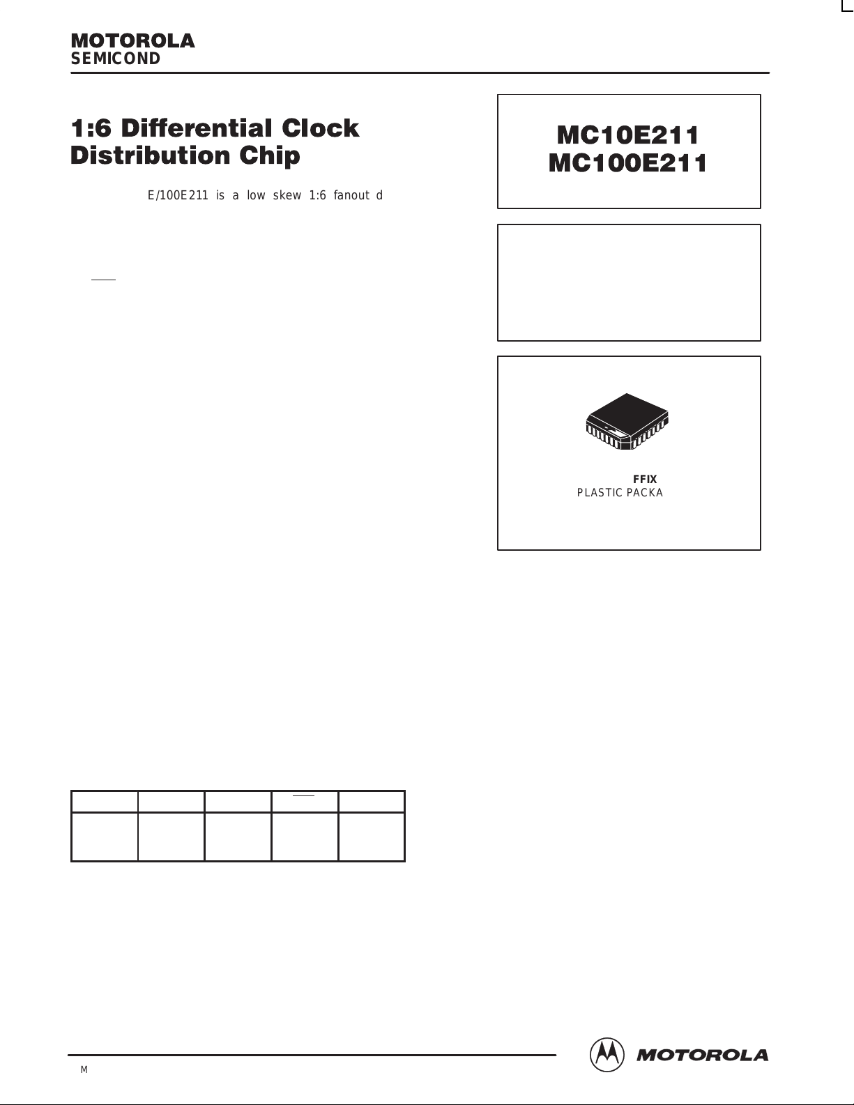
Both a common enable and individual output enables are provided. When asserted the positive output will go LOW on the next
negative transition of the CLK (or SCLK) input. The enabling function is synchronous so that the outputs will only be
enabled/disabled when the outputs are already in the LOW state. In this way the problem of runt pulse generation during the
disable operation is avoided. Note that the internal flip flop is clocked on the falling edge of the input clock edge, therefore all
associated specifications are referenced to the negative edge of the CLK input.
The output transitions of the E211 are faster than the standard ECLinPS edge rates. This feature provides a means of
distributing higher frequency signals than capable with the E111 device. Because of these edge rates and the tight skew limits
guaranteed in the specification, there are certain termination guidelines which must be followed. For more details on the
recommended termination schemes please refer to the applications information section of this data sheet.
FUNCTION TABLE
CLK SCLK SEL ENx Q
H/L
X
Z*
* Z = Negative transition of CLK or SCLK
X
H/L
Z*
L
H
X
L
L
H
CLK
SCLK
L
ECLinPS is a trademark of Motorola Inc.
5/95
Motorola, Inc. 1996
2–1
REV 3
MC10E211 MC100E211
EN3
SEL
SCLK
V
CLK
CLK
V
BB
EE
EN0
EN4 EN5 V
25
26
27
28
1
2
3
4
5
CEN
24
6
EN2
Q5 Q5 Q4 Q4
CC0
22
23
7
8
EN1
EN0
Pinout: 28-Lead PLCC (Top View)
21
CC0
19
20
18
Q3
17
Q3
16
V
CC
Q2
15
14
Q2
Q1
13
12
Q1
11109
Q0
Q0V
Q0
Q0
QD
CLK
CLK
SCLK
SEL
EN1-4
CEN
EN5
V
BB
0
1
BITS 1-4
Q1-4
Q1-4
QD
Q5
Q5
QD
Logic Diagram
MOTOROLA ECLinPS and ECLinPS Lite
2–2
DL140 — Rev 4
MC10E211 MC100E211
DC CHARACTERISTICS (VEE = VEE(min) to VEE(max); VCC = V
0°C 25°C 85°C
Characteristic Symbol Min Typ Max Min Typ Max Min Typ Max Unit Condition
Output Reference Voltage
10E
100E
Input High Current I
Power Supply Current
10E
100E
AC CHARACTERISTICS (V
Characteristic Symbol Min Typ Max Min Typ Max Min Typ Max Unit Condition
Propagation Delay to Output
CLK to Q (Diff)
CLK to Q (SE)
SCLK to Q
SEL to Q
Disable Time
CLK or SCLK to Q
Part–to–Part Skew
CLK (Diff) to Q
CLK (SE), SCLK to Q
Within-Device Skew
Setup Time
EN
x to CLK
to CLK
CEN
Hold Time
CLK to EN
Minimum Input Swing (CLK) V
Com. Mode Range (CLK) V
Rise/Fall Times
20 – 80%
1. Within-Device skew is defined for identical transitions on similar paths through a device.
2. Setup, Hold and Disable times are all relative to a falling edge on CLK or SCLK.
3. Minimum input swing for which AC parameters are guaranteed. Full DC ECL output swings will be generated with only 50mV input swings.
4. The range in which the high level of the input swing must fall while meeting the VPP spec. The lower end of the range is VEE dependent and
can be calculated as VEE + 2.4V.
x, CEN
V
BB
–1.38
–1.38
IH
I
EE
= VEE(min) to VEE(max); VCC = V
EE
t
PLH
t
PHL
t
PHL
t
skew
t
s
t
h
PP
CMR
t
r
t
f
119
119
0°C 25°C 85°C
795
930
745
930
650
900
745
970
600 800 600 800 600 800
50
200
–100
200
900 600 900 160 900 600
0.25 1.0 0.25 1.0 0.25 1.0 V 3
–0.4 Note –0.4 Note –0.4 Note V 4
150 400 150 400 150 400
0
–1.27
–1.35
–1.26
–1.38
150 150 150 µA
160
160
CCO
1065
1115
1085
1195
805
755
650
755
270
370
75
200
200
= GND)
CCO
119
119
= GND)
940
940
910
980
50
–100
–1.25
–1.31
–1.26
–1.38
160
160
1075
1125
1095
1205
0
825
775
650
775
270
370
75
200
200
119
137
960
960
930
1000
–100
0
–1.19
–1.26
160
164
1095
1145
1115
1225
270
370
75
V
mA
ps
ps
2
ps
1
ps
2
ps
2
ps
DL140 — Rev 4
2–3 MOTOROLAECLinPS and ECLinPS Lite

MC10E211 MC100E211
APPLICATIONS INFORMATION
General Description
The MC10E/100E211 is a 1:6 fanout tree designed
explicitly for low skew high speed clock distribution. The
device was targeted to work in conjunction with the E111
device to provide another level of flexibility in the design and
implementation of clock distribution trees. The individual
synchronous enable controls and multiplexed clock inputs
make the device ideal as the first level distribution unit in a
distribution tree. The device provides the ability to distribute a
lower speed scan or test clock along with the high speed
system clock to ease the design of system diagnostics and
self test procedures. The individual enables could be used to
allow for the disabling of individual cards on a backplane in
fault tolerant designs.
Because of lower fanout and larger skews the E211 will
not likely be used as an alternative to the E1 11 for the bulk of
the clock fanout generation. Figure 1 shows a typical
application combining the two devices to take advantage of
the strengths of each.
E211
Q0
Q5
E111
BACKPLANE
E111
Q0
Q8
Q0
Q8
Figure 1. Standard E211 Application
Using the E211 in PECL Designs
The E21 1 device can be utilized very effectively in designs
utilizing only a +5V power supply . Since the internal switching
reference levels are biased off of the VCC supply the input
thresholds for the single-ended inputs will vary with VCC. As a
result the single-ended inputs should be driven by a device
on the same board as the E21 1. Driving these inputs across a
backplane where significant differences between the VCC’s of
the transmitter and receiver can occur can lead to AC
performance and/or significant noise margin degradations.
Because the differential I/O does not use a switching
reference, and due to the CMR range of the E211, even
under worst case VCC situations between cards there will be
no AC performance or noise margin loss for the differential
CLK inputs.
For situations where TTL clocks are required the E21 1 can
be interfaced with the H641 or H643 ECL to TTL Clock
Distribution Chips from Motorola. The H641 is a single supply
1:9 PECL to TTL device while the H643 is a 1:8 dual supply
standard ECL to TTL device. By combining the superior skew
performance of the E211, or E111, with the low skew
translating capabilities of the H641 and H643 very low skew
TTL clock distribution networks can be realized.
Handling Open Inputs and Outputs
All of the input pins of the E211 have a 50kΩ to 75kΩ
pulldown resistor to pull the input to VEE when left open. This
feature can cause a problem if the differential clock inputs are
left open as the input gate current source transistor will
become saturated. Under these conditions the outputs of the
CLK input buffer will go to an undefined state. It is
recommended, if possible,that the SCLK input should be
selected any time the differential CLK inputs are allowed to
float. The SCLK buffer, under open input conditions, will
maintain a defined output state and thus the Q outputs of the
device will be in a defined state (Q = LOW). Note that if all of
the inputs are left open the differential CLK input will be
selected and the state of the Q outputs will be undefined.
With the simultaneous switching characteristics and the
tight skew specifications of the E211 the handling of the
unused outputs becomes critical. To minimize the noise
generated on the die all outputs should be terminated in
pairs, ie. both the true and compliment outputs should be
terminated even if only one of the outputs will be used in the
system. With both complimentary pairs terminated the
current in the VCC pins will remain essentially constant and
thus inductance induced voltage glitches on VCC will not
occur. VCC glitches will result in distorted output waveforms
and degradations in the skew performance of the device.
The package parasitics of the 28-lead PLCC cause the
signals on a given pin to be influenced by signals on adjacent
pins. The E211 is characterized and tested with all of the
outputs switching, therefore the numbers in the data book are
guaranteed only for this situation. If all of the outputs of the
E21 1 are not needed and there is a desire to save power the
unused output pairs can be left unterminated. Unterminated
outputs can influence the propagation delay on adjacent pins
by 15ps - 20ps. Therefore under these conditions this 15ps 20ps needs to be added to the overall skew of the device.
Pins which are separated by a package corner are not
considered adjacent pins in the context of propagation delay
influence. Therefore as long as all of the outputs on a single
side of the package are terminated the specification limits in
the data sheet will apply.
MOTOROLA ECLinPS and ECLinPS Lite
2–4
DL140 — Rev 4

APPLICATIONS INFORMATION
MC10E211 MC100E211
Differential versus Single-Ended Use
As can be seen from the data sheet, to minimize the skew
of the E21 1 the device must be used in the dif ferential mode.
In the single-ended mode the propagation delays are
dependent on the relative position of the VBB switching
reference. Any VBB offset from the center of the input swing
will add delay to either the T
PLH
or T
and subtract delay
PHL
from the other. This increase and decrease in delay will lead
to an increase in the duty cycle skew and thus part-to-part
skew. The within-device skew will be independent of the V
BB
and therefore will be the same regardless of whether the
device is driven differentially or single-endedly.
For applications where part-to-part skew or duty cycle
skew are not important the advantages of single-ended clock
distribution may lead to its use. Using single-ended
interconnect will reduce the number of signal traces to be
routed, but remember that all of the complimentary outputs
still need to be terminated therefore there will be no reduction
in the termination components required. T o use the E21 1 with
a single-ended input the arrangement pictured in Figure 2b
should be used. If the input to the differential CLK inputs are
AC coupled as pictured in Figure 2a the dependence on a
centered VBB reference is removed. The situation pictured
will ensure that the input is centered around the bias set by
the VBB. As a result when AC coupled the AC specification
limits for a differential input can be used. For more
information on AC coupling please refer to the interfacing
section of the design guide in the ECLinPS data book.
pulse. On initial power up the enable flip flops will randomly
attain a stable state, therefore precautions should be taken
on initial power up to ensure the E21 1 is in the desired state.
IN
0.001µF
IN
50Ω
0.01µF
V
BB
Figure 2a. AC Coupled Input
IN
IN
Using the Enable Pins
Both the common enable (CEN
enables (ENx
) are synchronous to the CLK or SCLK input
) and the individual
depending on which is selected. The active low signals are
clocked into the enable flip flops on the negative edges of the
E211 clock inputs. In this way the devices will only be
disabled when the outputs are already in the LOW state. The
internal propagation delays are such that the delay to the
output through the distribution buffers is less than that
through the enable flip flops. This will ensure that the
disabling of the device will not slice any time off the clock
0.01µF
V
BB
Figure 2b. Single-Ended Input
DL140 — Rev 4
2–5 MOTOROLAECLinPS and ECLinPS Lite

MC10E211 MC100E211
-N-
-L-
28 1
OUTLINE DIMENSIONS
FN SUFFIX
PLASTIC PLCC PACKAGE
CASE 776–02
ISSUE D
SNSM
G1
–M
SNSM
–M
0.010 (0.250) T L
–M
SNSS
0.007 (0.180) T L
Y BRK
B
0.007 (0.180) T L
U
D
Z
-M-
D
W
V
X
VIEW D-D
Z
C
G
G1
0.010 (0.250) T L
0.007 (0.180) T L
A
0.007 (0.180) T L
R
E
0.004 (0.100)
J
PLANE
SEATING
-T-
VIEW S
SNSS
–M
NOTES:
1. DATUMS -L-, -M-, AND -N- DETERMINED
WHERE TOP OF LEAD SHOULDER EXITS
PLASTIC BODY AT MOLD PARTING LINE.
2. DIM G1, TRUE POSITION TO BE MEASURED
AT DATUM -T-, SEATING PLANE.
3. DIM R AND U DO NOT INCLUDE MOLD FLASH.
ALLOWABLE MOLD FLASH IS 0.010 (0.250)
PER SIDE.
4. DIMENSIONING AND TOLERANCING PER ANSI
Y14.5M, 1982.
5. CONTROLLING DIMENSION: INCH.
6. THE PACKAGE TOP MAY BE SMALLER THAN
THE PACKAGE BOTTOM BY UP TO 0.012
(0.300). DIMENSIONS R AND U ARE
DETERMINED AT THE OUTERMOST
EXTREMES OF THE PLASTIC BODY
EXCLUSIVE OF MOLD FLASH, TIE BAR
BURRS, GATE BURRS AND INTERLEAD
FLASH, BUT INCLUDING ANY MISMATCH
BETWEEN THE TOP AND BOTTOM OF THE
PLASTIC BODY.
7. DIMENSION H DOES NOT INCLUDE DAMBAR
PROTRUSION OR INTRUSION. THE DAMBAR
PROTRUSION(S) SHALL NOT CAUSE THE H
DIMENSION TO BE GREATER THAN 0.037
(0.940). THE DAMBAR INTRUSION(S) SHALL
NOT CAUSE THE H DIMENSION TO BE
SMALLER THAN 0.025 (0.635).
–M
–M
SNSM
SNSM
H
0.007 (0.180) T L
–M
SNSM
K1
K
SNSM
0.007 (0.180) T L
F
–M
VIEW S
INCHES MILLIMETERS
MIN MINMAX MAX
DIM
A
0.485
B
0.485
C
0.165
E
0.090
F
0.013
G
0.050 BSC
H
0.026
J
0.020
K
0.025
R
0.450
U
0.450
V
0.042
W
0.042
X
0.042
Y
—
Z
2°
G1
0.410
K1
0.040
0.495
0.495
0.180
0.110
0.019
0.032
0.456
0.456
0.048
0.048
0.056
0.020
10°
0.430
12.32
12.57
12.32
12.57
4.20
4.57
2.29
2.79
0.33
0.48
1.27 BSC
0.66
0.81
0.51
0.64
11.43
11.43
1.07
1.07
1.07
10.42
1.02
—
—
11.58
11.58
1.21
1.21
1.42
—
0.50
2°
10°
10.92
—
—
—
—
MOTOROLA ECLinPS and ECLinPS Lite
2–6
DL140 — Rev 4

MC10E211 MC100E211
Motorola reserves the right to make changes without further notice to any products herein. Motorola makes no warranty , representation or guarantee regarding
the suitability of its products for any particular purpose, nor does Motorola assume any liability arising out of the application or use of any product or circuit, and
specifically disclaims any and all liability, including without limitation consequential or incidental damages. “T ypical” parameters which may be provided in Motorola
data sheets and/or specifications can and do vary in different applications and actual performance may vary over time. All operating parameters, including “Typicals”
must be validated for each customer application by customer’s technical experts. Motorola does not convey any license under its patent rights nor the rights of
others. Motorola products are not designed, intended, or authorized for use as components in systems intended for surgical implant into the body, or other
applications intended to support or sustain life, or for any other application in which the failure of the Motorola product could create a situation where personal injury
or death may occur. Should Buyer purchase or use Motorola products for any such unintended or unauthorized application, Buyer shall indemnify and hold Motorola
and its officers, employees, subsidiaries, affiliates, and distributors harmless against all claims, costs, damages, and expenses, and reasonable attorney fees
arising out of, directly or indirectly, any claim of personal injury or death associated with such unintended or unauthorized use, even if such claim alleges that
Motorola was negligent regarding the design or manufacture of the part. Motorola and are registered trademarks of Motorola, Inc. Motorola, Inc. is an Equal
Opportunity/Affirmative Action Employer.
How to reach us:
USA/EUROPE/Locations Not Listed: Motorola Literature Distribution; JAPAN: Nippon Motorola Ltd.; Tatsumi–SPD–JLDC, 6F Seibu–Butsuryu–Center,
P.O. Box 20912; Phoenix, Arizona 85036. 1–800–441–2447 or 602–303–5454 3–14–2 Tatsumi Koto–Ku, Tokyo 135, Japan. 03–81–3521–8315
MFAX: RMF AX0@email.sps.mot.com – T OUCHTONE 602–244–6609 ASIA/PACIFIC: Motorola Semiconductors H.K. Ltd.; 8B Tai Ping Industrial Park,
INTERNET: http://Design–NET .com 51 Ting Kok Road, Tai Po, N.T., Hong Kong. 852–26629298
MC10E211/D
DL140 — Rev 4
◊
2–7 MOTOROLAECLinPS and ECLinPS Lite
*MC10E211/D*
 Loading...