

SEMICONDUCTOR TECHNICAL DATA
2–1
REV 2
Motorola, Inc. 1996
12/93
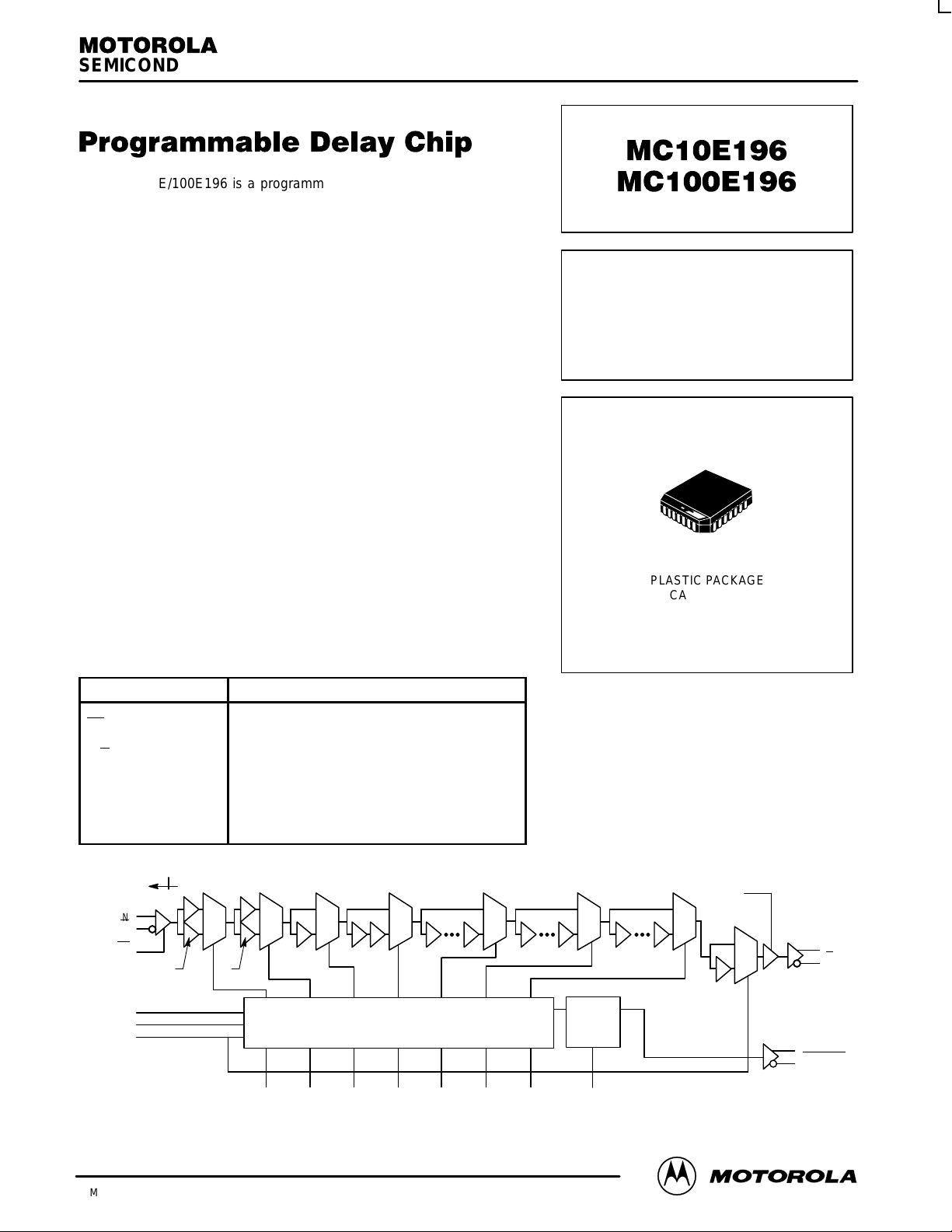
The MC10E/100E196 is a programmable delay chip (PDC) designed
primarily for very accurate differential ECL input edge placement
applications.
The delay section consists of a chain of gates and a linear ramp delay
adjust organized as shown in the logic symbol. The first two delay
elements feature gates that have been modified to have delays 1.25 and
1.5 times the basic gate delay of approximately 80 ps. These two
elements provide the E196 with a digitally-selectable resolution of
approximately 20 ps. The required device delay is selected by the seven
address inputs D[0:6], which are latched on chip by a high signal on the
latch enable (LEN) control.
The FTUNE input takes an analog voltage and applies it to an internal
linear ramp for reducing the 20 ps resolution still further. The FTUNE input
is what differentiates the E196 from the E195.
An eighth latched input, D7, is provided for cascading multiple PDC’s
for increased programmable range. The cascade logic allows full control
of multiple PDC’s, at the expense of only a single added line to the data
bus for each additional PDC, without the need for any external gating.
• 2.0ns Worst Case Delay Range
• ≈20ps/Delay Step Resolution
• Linear Input for Tighter Resolution
• >1.0GHz Bandwidth
• On Chip Cascade Circuitry
• Extended 100E V
EE
Range of –4.2 to –5.46V
• 75KΩ Input Pulldown Resistors
PIN NAMES
Pin Function
IN/IN
EN
D[0:7]
Q/Q
LEN
SET MIN
SET MAX
CASCADE
FTUNE
Signal Input
Input Enable
Mux Select Inputs
Signal Output
Latch Enable
Min Delay Set
Max Delay Set
Cascade Signal
Linear Voltage Input
1
LOGIC DIAGRAM – SIMPLIFIED
V
BB
IN
IN
EN
LEN
SET MIN
SET MAX
110
1
0
1
0
1
0
1
0
1
0
1
0
1 1 1
101
Q
Q
CASCADE
CASCADE
CASCADE
7 BIT LATCH
LEN Q
LATCH
D
4 GATES 8 GATES 16 GATES
* 1.25
* 1.5
D0 D1 D2 D3 D4 D5 D6 D7
* DELAYS ARE 25% OR 50% LONGER THAN
* STANDARD (STANDARD
≈
80 PS)
LINEAR
RAMP
FTUNE
PROGRAMMABLE
DELAY CHIP
FN SUFFIX
PLASTIC PACKAGE
CASE 776-02
MC10E196 MC100E196
MOTOROLA ECLinPS and ECLinPS Lite
DL140 — Rev 4
2–2
D2
D3 D4 D5 D6 D7 NC
NC NC EN
SET MIN
SET MAX
CASCADE
CASCADE
FTUNE
NC
V
CC
V
CCO
Q
Q
V
CCO
D1
D0
LEN
V
EE
IN
IN
V
BB
25 24 23 22 21 20 19
26
27
28
1
2
3
4
18
17
16
15
14
13
12
5 6 7 8 9 10 11
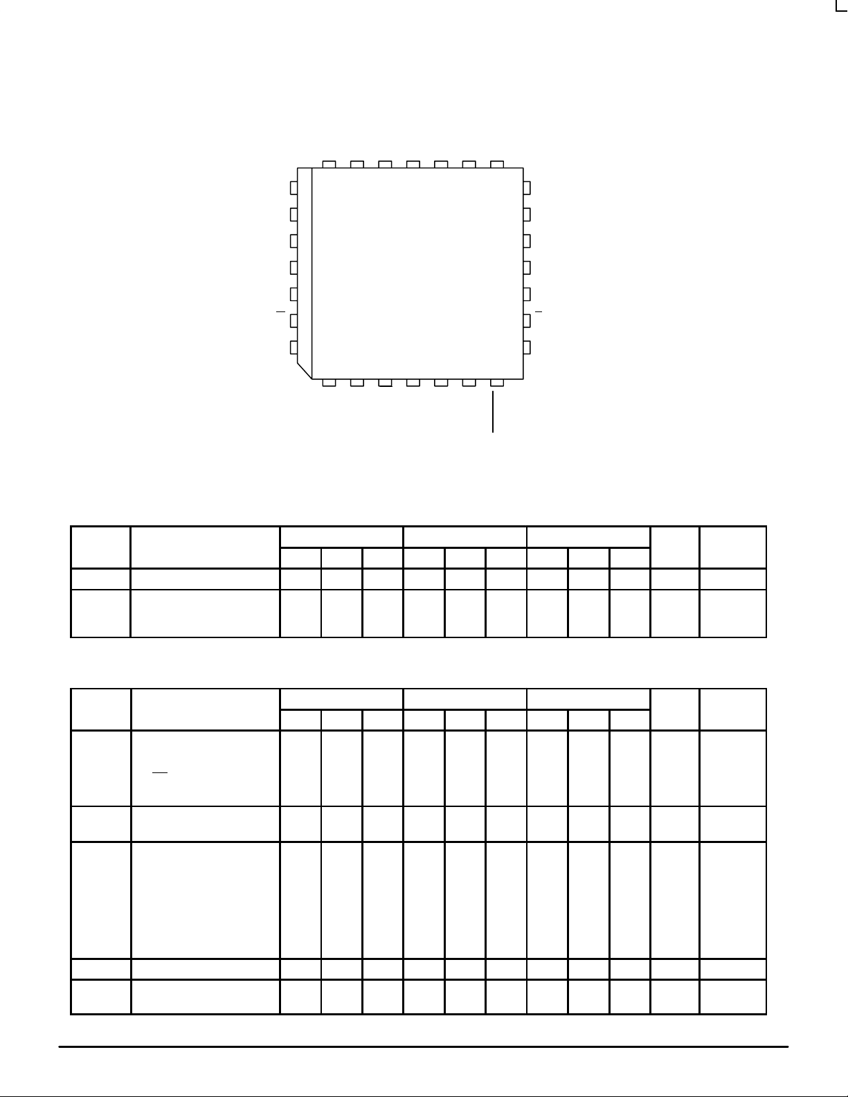
Pinout: 28-Lead PLCC (Top View)
DC CHARACTERISTICS (VEE = VEE(min) to VEE(max); VCC = V
CCO
= GND)
0°C 25°C 85°C
Symbol Characteristic Min Typ Max Min Typ Max Min Typ Max Unit Condition
I
IH
Input HIGH Current 150 150 150 µA
I
EE
Power Supply Current
10E
100E
130
130
156
156
130
130
156
156
130
150
156
179
mA
AC CHARACTERISTICS (VEE = VEE(min) to VEE(max); VCC = V
CCO
= GND)
0°C 25°C 85°C
Symbol Characteristic Min Typ Max Min Typ Max Min Typ Max Unit Notes
t
PLH
t
PHL
Propagation Delay
IN to Q; Tap = 0
IN to Q; Tap = 127
EN
to Q; Tap = 0
D7 to CASCADE
1210
3320
1250
300
1360
3570
1450
450
1510
3820
1650
700
1240
3380
1275
300
1390
3630
1475
450
1540
3880
1675
700
1440
3920
1350
300
1590
4270
1650
450
1765
4720
1950
700
ps
t
RANGE
Programmable Range
tPD (max) – tPD (min)
2000 2175 2050 2240 2375 2580
ps
∆t Step Delay
D0 High
D1 High
D2 High
D3 High
D4 High
D5 High
D6 High
55
115
250
505
1000
17
34
68
136
272
544
1088
105
180
325
620
1190
55
115
250
515
1030
17.5
35
70
140
280
560
1120
105
180
325
620
1220
65
140
305
620
1240
21
42
84
168
336
672
1344
120
205
380
740
1450
ps 6
Lin Linearity D1 D0 D1 D0 D1 D0 7
t
SKEW
Duty Cycle Skew
t
PHL–tPLH
±30 ±30 ±30
ps
1
MC10E196 MC100E196
2–3 MOTOROLAECLinPS and ECLinPS Lite
DL140 — Rev 4
AC CHARACTERISTICS (continued) (VEE = VEE(min) to VEE(max); VCC = V
CCO
= GND)
0°C 25°C 85°C
Symbol Characteristic Min Typ Max Min Typ Max Min Typ Max Unit Notes
t
s
Setup Time
D to LEN
D to IN
EN
to IN
200
800
200
0 200
800
200
0 200
800
200
0
ps
2
3
t
h
Hold Time
LEN to D
IN to EN
5000250 5000250 5000250
ps
4
t
R
Release Time
EN
to IN
SET MAX to LEN
SET MIN to LEN
300
800
800
300
800
800
300
800
800
ps
5
t
jit
Jitter <5.0 <5.0 <5.0 ps 8
t
r
t
f
Output Rise/Fall Time
20–80% (Q)
20–80% (CASCADE)
125
300
225
450
325
650
125
300
225
450
325
650
125
300
225
450
325
650
ps
1. Duty cycle skew guaranteed only for differential operation measured from the cross point of the input to the cross point of the output.
2. This setup time defines the amount of time prior to the input signal the delay tap of the device must be set.
3. This setup time is the minimum time that EN
must be asserted prior to the next transition of IN/IN to prevent an output response greater than
±75 mV to that IN/IN
transition.
4. This hold time is the minimum time that EN
must remain asserted after a negative going IN or positive going IN to prevent an output response
greater than ±75 mV to that IN/IN transition.
5. This release time is the minimum time that EN
must be deasserted prior to the next IN/IN transition to ensure an output response that meets
the specified IN to Q propagation delay and transition times.
6. Specification limits represent the amount of delay added with the assertion of each individual delay control pin. The various combinations of
asserted delay control inputs will typically realize D0 resolution steps across the specified programmable range.
7. The linearity specification guarantees to which delay control input the programmable steps will be monotonic (i.e. increasing delay steps for
increasing binary counts on the control inputs Dn). Typically the device will be monotonic to the D0 input, however under worst case conditions
and process variation, delays could decrease slightly with increasing binary counts when the D0 input is the LSB. With the D1 input as the LSB
the device is guaranteed to be monotonic over all specified environmental conditions and process variation.
8. The jitter of the device is less than what can be measured without resorting to very tedious and specialized measurement techniques.
ANALOG INPUT CHARACTERISTICS
Ftune = VCC to V
EE
140
120
100
80
60
40
20
0
–4.5 –3.5 –2.5 –1.5 –0.5
PROPAGATION DELAY (ps)
Propagation Delay versus Ftune Voltage
(100E196)
FTUNE VOLTAGE (V)
100
90
80
70
60
50
40
30
20
10
0
–5 –4 –3 –2 –1 0
PROPAGATION DELAY (ps)
Propagation Delay versus Ftune Voltage
(10E196)
FTUNE VOLTAGE (V)

MC10E196 MC100E196
MOTOROLA ECLinPS and ECLinPS Lite
DL140 — Rev 4
2–4
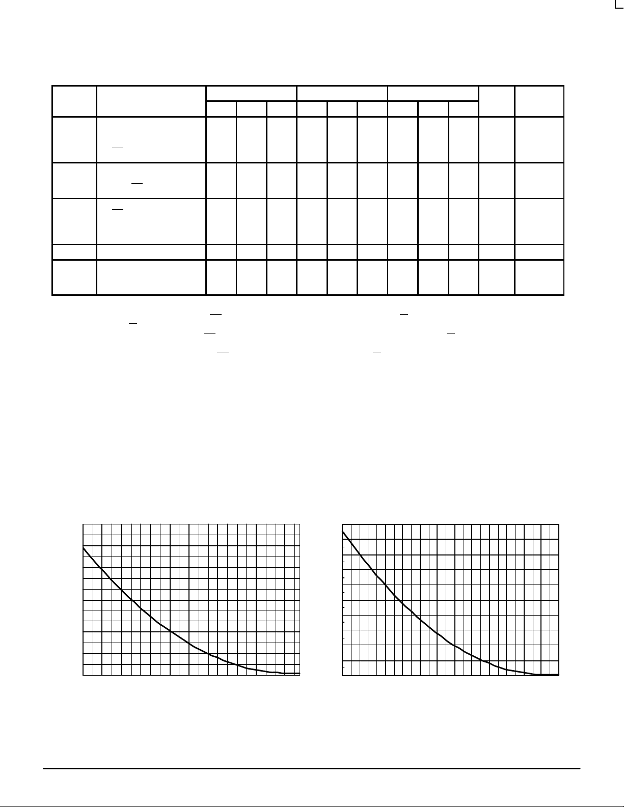
USING THE FTUNE ANALOG INPUT
The analog FTUNE pin on the E196 device is intended to
enhance the 20 ps resolution capabilities of the fully digital
E195. The level of resolution obtained is dependent on the
number of increments applied to the appropriate range on the
FTUNE pin.
To provide another level of resolution the FTUNE pin must
be capable of adjusting the delay by greater than the 20 ps
digital resolution. From the provided graphs one sees that this
requirement is easily achieved as over the entire FTUNE
voltage range a 100 ps delay can be achieved. This extra
analog range ensures that the FTUNE pin will be capable even
under worst case conditions of covering the digital
resolution.Typically the analog input will be driven by an
external DAC to provide a digital control with very fine analog
output steps. The final resolution of the device will be
dependent on the width of the DAC chosen.
To determine the voltage range necessary for the FTUNE
input, the graphs provided should be used. As an example if a
range of 40 ps is selected to cover worst case conditions and
ensure coverage of the digital range, from the 100E196 graph
a voltage range of –3.25 V to –4.0 V would be necessary on the
FTUNE pin. Obviously there are numerous voltage ranges
which can be used to cover a given delay range, users are
given the flexibility to determine which one best fits their
designs.
Cascading Multiple E196’s
To increase the programmable range of the E195 internal
cascade circuitry has been included. This circuitry allows for
the cascading of multiple E195’s without the need for any
external gating. Furthermore this capability requires only one
more address line per added E195. Obviously cascading
multiple PDC’s will result in a larger programmable range,
however, this increase is at the expense of a longer minimum
delay.
Figure 1 illustrates the interconnect scheme for cascading
two E195’s. As can be seen, this scheme can easily be
expanded for larger E195 chains. The D7 input of the E195 is
the cascade control pin. With the interconnect scheme of
Figure 1 when D7 is asserted it signals the need for a larger
programmable range than is achievable with a single device.
An expansion of the latch section of the block diagram is
pictured below. Use of this diagram will simplify the
explanation of how the cascade circuitry works. When D7 of
chip #1 above is low the cascade output will also be low while
the cascade bar output will be a logical high. In this condition
the SET MIN pin of chip #2 will be asserted and thus all of the
latches of chip #2 will be reset and the device will be set at its
minimum delay. Since the RESET and SET inputs of the
latches are overriding any changes on the A0–A6 address bus
will not affect the operation of chip #2.
Chip #1 on the other hand will have both SET MIN and SET
MAX de-asserted so that its delay will be controlled entirely by
the address bus A0–A6. If the delay needed is greater than
can be achieved with 31.75 gate delays (1111111 on the
A0–A6 address bus) D7 will be asserted to signal the need to
cascade the delay to the next E195 device. When D7 is
asserted the SET MIN pin of chip #2 will be de-asserted and
the delay will be controlled by the A0–A6 address bus. Chip #1
on the other hand will have its SET MAX pin asserted
resulting in the device delay to be independent of the A0–A6
address bus.
When the SET MAX pin of chip #1 is asserted the D0 and D1
latches will be reset while the rest of the latches will be set. In
addition, to maintain monotonicity an additional gate delay is
selected in the cascade circuitry . As a result when D7 of chip
#1 is asserted the delay increases from 31.75 gates to 32
gates. A 32 gate delay is the maximum delay setting for
the E195.
When cascading multiple PDC’s it will prove more cost
effective to use a single E196 for the MSB of the chain while
using E195 for the lower order bits. This is due to the fact that
only one fine tune input is needed to further reduce the delay
step resolution.
ADDRESS BUS (A0–A6)
A7
INPUT
D1
D0
LEN
V
EE
IN
IN
V
BB
D2D3D4D5D6
D7
EN
SET MIN
SET MAX
CASCADE
CASCADE
V
CC
V
CC0
Q
Q
V
CC0
D1
D0
LEN
V
EE
IN
IN
V
BB
EN
SET MIN
SET MAX
CASCADE
CASCADE
V
CC
V
CC0
Q
Q
V
CC0
OUTPUT
D2D3D4D5D6
D7
E196
Chip #1
E196
Chip #2
Figure 1. Cascading Interconnect Architecture
FTUNE
LINEAR
INPUT
FTUNE

MC10E196 MC100E196
2–5 MOTOROLAECLinPS and ECLinPS Lite
DL140 — Rev 4
SET MIN
SET MAX
TO SELECT MULTIPLEXERS
BIT 0 BIT 1 BIT 2 BIT 3 BIT 4 BIT 5 BIT 6 BIT 7
D0 Q0
LEN
Reset Reset
D1 Q1 D2 Q2 D3 Q3 D4 Q4 D5 Q5
D6 Q6 D7 Q7
LEN LEN LEN LEN LEN LEN LEN
CASCADE
CASCADE
Figure 2. Expansion of the Latch Section of the E195 Block Diagram
Reset Reset Reset Reset Reset Reset Reset Reset Reset Reset
Reset Reset Reset Reset

MC10E196 MC100E196
MOTOROLA ECLinPS and ECLinPS Lite
DL140 — Rev 4
2–6
OUTLINE DIMENSIONS
FN SUFFIX
PLASTIC PLCC PACKAGE
CASE 776–02
ISSUE D
0.007 (0.180) T L
–M
SNSM
0.007 (0.180) T L
–M
SNSM
0.007 (0.180) T L
–M
SNSM
0.010 (0.250) T L
–M
SNSS
0.007 (0.180) T L
–M
SNSM
0.010 (0.250) T L
–M
SNSS
0.007 (0.180) T L
–M
SNSM
0.007 (0.180) T L
–M
SNSM
0.004 (0.100)
SEATING
PLANE
-T-
12.32
12.32
4.20
2.29
0.33
0.66
0.51
0.64
11.43
11.43
1.07
1.07
1.07
—
2
°
10.42
1.02
12.57
12.57
4.57
2.79
0.48
0.81
—
—
11.58
11.58
1.21
1.21
1.42
0.50
10
°
10.92
—
1.27 BSC
A
B
C
E
F
G
H
J
K
R
U
V
W
X
Y
Z
G1
K1
MIN MINMAX MAX
INCHES MILLIMETERS
DIM
NOTES:
1. DATUMS -L-, -M-, AND -N- DETERMINED
WHERE TOP OF LEAD SHOULDER EXITS
PLASTIC BODY AT MOLD PARTING LINE.
2. DIM G1, TRUE POSITION TO BE MEASURED
AT DATUM -T-, SEATING PLANE.
3. DIM R AND U DO NOT INCLUDE MOLD FLASH.
ALLOWABLE MOLD FLASH IS 0.010 (0.250)
PER SIDE.
4. DIMENSIONING AND TOLERANCING PER ANSI
Y14.5M, 1982.
5. CONTROLLING DIMENSION: INCH.
6. THE PACKAGE TOP MAY BE SMALLER THAN
THE PACKAGE BOTTOM BY UP TO 0.012
(0.300). DIMENSIONS R AND U ARE
DETERMINED AT THE OUTERMOST
EXTREMES OF THE PLASTIC BODY
EXCLUSIVE OF MOLD FLASH, TIE BAR
BURRS, GATE BURRS AND INTERLEAD
FLASH, BUT INCLUDING ANY MISMATCH
BETWEEN THE TOP AND BOTTOM OF THE
PLASTIC BODY.
7. DIMENSION H DOES NOT INCLUDE DAMBAR
PROTRUSION OR INTRUSION. THE DAMBAR
PROTRUSION(S) SHALL NOT CAUSE THE H
DIMENSION TO BE GREATER THAN 0.037
(0.940). THE DAMBAR INTRUSION(S) SHALL
NOT CAUSE THE H DIMENSION TO BE
SMALLER THAN 0.025 (0.635).
VIEW S
B
U
Z
G1
X
VIEW D-D
H
K
F
VIEW S
G
C
Z
A
R
E
J
0.485
0.485
0.165
0.090
0.013
0.026
0.020
0.025
0.450
0.450
0.042
0.042
0.042
—
2
°
0.410
0.040
0.495
0.495
0.180
0.110
0.019
0.032
—
—
0.456
0.456
0.048
0.048
0.056
0.020
10
°
0.430
—
0.050 BSC
-N-
Y BRK
D
D
W
-M-
-L-
28 1
V
G1
K1

MC10E196 MC100E196
2–7 MOTOROLAECLinPS and ECLinPS Lite
DL140 — Rev 4
Motorola reserves the right to make changes without further notice to any products herein. Motorola makes no warranty , representation or guarantee regarding
the suitability of its products for any particular purpose, nor does Motorola assume any liability arising out of the application or use of any product or circuit, and
specifically disclaims any and all liability , including without limitation consequential or incidental damages. “Typical” parameters which may be provided in Motorola
data sheets and/or specifications can and do vary in different applications and actual performance may vary over time. All operating parameters, including “Typicals”
must be validated for each customer application by customer’s technical experts. Motorola does not convey any license under its patent rights nor the rights of
others. Motorola products are not designed, intended, or authorized for use as components in systems intended for surgical implant into the body, or other
applications intended to support or sustain life, or for any other application in which the failure of the Motorola product could create a situation where personal injury
or death may occur. Should Buyer purchase or use Motorola products for any such unintended or unauthorized application, Buyer shall indemnify and hold Motorola
and its officers, employees, subsidiaries, affiliates, and distributors harmless against all claims, costs, damages, and expenses, and reasonable attorney fees
arising out of, directly or indirectly, any claim of personal injury or death associated with such unintended or unauthorized use, even if such claim alleges that
Motorola was negligent regarding the design or manufacture of the part. Motorola and are registered trademarks of Motorola, Inc. Motorola, Inc. is an Equal
Opportunity/Affirmative Action Employer.
How to reach us:
USA/EUROPE/Locations Not Listed: Motorola Literature Distribution; JAPAN: Nippon Motorola Ltd.; Tatsumi–SPD–JLDC, 6F Seibu–Butsuryu–Center,
P.O. Box 20912; Phoenix, Arizona 85036. 1–800–441–2447 or 602–303–5454 3–14–2 Tatsumi Koto–Ku, Tokyo 135, Japan. 03–81–3521–8315
MFAX: RMFAX0@email.sps.mot.com – TOUCHTONE 602–244–6609 ASIA/PACIFIC: Motorola Semiconductors H.K. Ltd.; 8B Tai Ping Industrial Park,
INTERNET: http://Design–NET.com 51 Ting Kok Road, Tai Po, N.T., Hong Kong. 852–26629298
MC10E196/D
*MC10E196/D*
◊

WWW.ALLDATASHEET.COM
Copyright © Each Manufacturing Company.
All Datasheets cannot be modified without permission.
This datasheet has been download from :
www.AllDataSheet.com
100% Free DataSheet Search Site.
Free Download.
No Register.
Fast Search System.
www.AllDataSheet.com
 Loading...