

MOTOROLA MC10E195FNR2, MC100E195FNR2 Datasheet

SEMICONDUCTOR TECHNICAL DATA
Order this document
by MC10E195/D
The MC10E/100E195 is a programmable delay chip (PDC) designed
primarily for clock de-skewing and timing adjustment. It provides variable
delay of a differential ECL input transition.
The delay section consists of a chain of gates organized as shown in
the logic symbol. The first two delay elements feature gates that have
been modified to have delays 1.25 and 1.5 times the basic gate delay of
approximately 80 ps. These two elements provide the E195 with a
digitally-selectable resolution of approximately 20 ps. The required
device delay is selected by the seven address inputs D[0:6], which are
latched on chip by a high signal on the latch enable (LEN) control.
Because the delay programmability of the E195 is achieved by purely
differential ECL gate delays the device will operate at frequencies of >1.0
GHz while maintaining over 600 mV of output swing.
The E195 thus offers very fine resolution, at very high frequencies, that
is selectable entirely from a digital input allowing for very accurate system
clock timing.
An eighth latched input, D7, is provided for cascading multiple PDC’s
for increased programmable range. The cascade logic allows full control
of multiple PDC’s, at the expense of only a single added line to the data
bus for each additional PDC, without the need for any external gating.
• 2.0ns Worst Case Delay Range
• ≈20ps/Delay Step Resolution
• >1.0GHz Bandwidth
• On Chip Cascade Circuitry
• Extended 100E V
• 75KΩ Input Pulldown Resistors
PIN NAMES
Pin Function
IN/IN
EN
D[0:7]
Q/Q
LEN
SET MIN
SET MAX
CASCADE
Range of –4.2 to –5.46V
EE
Signal Input
Input Enable
Mux Select Inputs
Signal Output
Latch Enable
Min Delay Set
Max Delay Set
Cascade Signal
PROGRAMMABLE
DELAY CHIP
FN SUFFIX
PLASTIC PACKAGE
CASE 776-02
D2
D3 D4 D5 D6 D7 NC
25 24 23 22 21 20 19
D1
26
D0
27
LEN
28
V
EE
1
IN
2
IN
3
V
4
BB
567891011
NC NC EN
Pinout:
28-Lead PLCC
(Top View)
SET MIN
SET MAX
18
NC
17
NC
16
V
CC
15
V
CCO
14
Q
13
Q
12
V
CCO
CASCADE
CASCADE
V
BB
1
* 1.25
110
* 1.5
IN
IN
EN
LEN
SET MIN
SET MAX
* DELAYS ARE 25% OR 50% LONGER THAN
* STANDARD (STANDARD ≈ 80 PS)
04/99
0
1
D0 D1 D2 D3 D4 D5 D6 D7
Motorola, Inc. 1999
LOGIC DIAGRAM – SIMPLIFIED
0
1
111
2–1
0
1
7 BIT LATCH
4 GATES 8 GATES 16 GATES
0
1
0
1
LEN Q
LATCH
D
REV 3
0
1
CASCADE
0
1
1
Q
Q
CASCADE
CASCADE
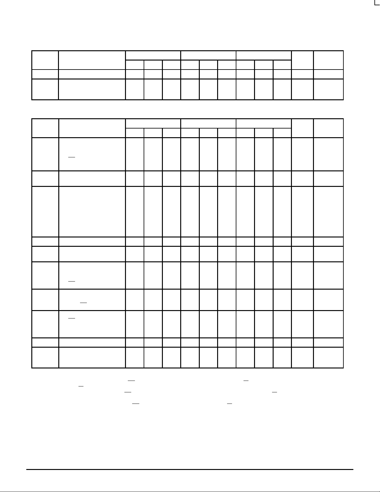
MC10E195 MC100E195
DC CHARACTERISTICS (VEE = VEE(min) to VEE(max); VCC = V
0°C 25°C 85°C
Symbol Characteristic Min Typ Max Min Typ Max Min Typ Max Unit Condition
I
I
IH
EE
Input HIGH Current 150 150 150 µA
Power Supply Current
10E
100E
130
130
156
156
AC CHARACTERISTICS (VEE = VEE(min) to VEE(max); VCC = V
0°C 25°C 85°C
Symbol Characteristic Min Typ Max Min Typ Max Min Typ Max Unit Notes
t
PLH
t
PHL
t
RANGE
∆t Step Delay
Lin Linearity D1 D0 D1 D0 D1 D0 7
t
SKEW
t
s
t
h
t
R
t
jit
t
r
t
f
1. Duty cycle skew guaranteed only for differential operation measured from the cross point of the input to the cross point of the output.
2. This setup time defines the amount of time prior to the input signal the delay tap of the device must be set.
3. This setup time is the minimum time that EN
±75 mV to that IN/IN
4. This hold time is the minimum time that EN
greater than ±75 mV to that IN/IN transition.
5. This release time is the minimum time that EN
the specified IN to Q propagation delay and transition times.
6. Specification limits represent the amount of delay added with the assertion of each individual delay control pin. The various combinations of
asserted delay control inputs will typically realize D0 resolution steps across the specified programmable range.
7. The linearity specification guarantees to which delay control input the programmable steps will be monotonic (i.e. increasing delay steps for
increasing binary counts on the control inputs Dn). Typically the device will be monotonic to the D0 input, however under worst case conditions
and process variation, delays could decrease slightly with increasing binary counts when the D0 input is the LSB. With the D1 input as the LSB
the device is guaranteed to be monotonic over all specified environmental conditions and process variation.
8. The jitter of the device is less than what can be measured without resorting to very tedious and specialized measurement techniques.
Propagation Delay
IN to Q; Tap = 0
IN to Q; Tap = 127
EN
to Q; Tap = 0
D7 to CASCADE
Programmable Range
tPD (max) – tPD (min)
D0 High
D1 High
D2 High
D3 High
D4 High
D5 High
D6 High
Duty Cycle Skew
t
PHL–tPLH
Setup Time
D to LEN
D to IN
EN
to IN
Hold Time
LEN to D
IN to EN
Release Time
EN
to IN
SET MAX to LEN
SET MIN to LEN
Jitter <5.0 <5.0 <5.0 ps 8
Output Rise/Fall Time
20–80% (Q)
20–80% (CASCADE)
transition.
1210
1360
1510
3200
3570
1250
1450
300
450
2000 2175 2050 2240 2375 2580
17
55
115
250
505
1000
200
800
200
5000250 5000250 5000250
300
800
800
125
300
must remain asserted after a negative going IN or positive going IN to prevent an output response
34
68
136
272
544
1088
±30 ±30 ±30
0 200
225
450
must be asserted prior to the next transition of IN/IN to prevent an output response greater than
must be deasserted prior to the next IN/IN transition to ensure an output response that meets
3970
1650
700
105
180
325
620
1190
325
650
1240
3270
1275
300
55
115
250
515
1030
800
200
300
800
800
125
300
= GND)
CCO
130
130
CCO
1390
3630
1475
450
17.5
140
280
560
1120
225
450
156
156
= GND)
1540
4030
1675
700
35
70
105
180
325
620
1220
0 200
325
650
1440
3885
1350
300
65
140
305
620
1240
800
200
300
800
800
125
300
130
150
1590
4270
1650
450
21
42
84
168
336
672
1344
0
225
450
156
mA
179
ps
1765
4710
1950
700
ps
ps 6
120
205
380
740
1450
ps
1
ps
2
3
ps
4
ps
5
ps
325
650
MOTOROLA ECLinPS and ECLinPS Lite
2–2
DL140 — Rev 4
 Loading...