


HFBR-5113FDA
HP HFBR-5113FDA, HFBR-5112FDS, HFBR-5112FDN, HFBR-5112FDM, HFBR-5112FDB Datasheet
...
92
Low Cost, Industry Standard
FDDI MIC Transceivers
Technical Data
HFBR-5111 (2x11)
HFBR-5112 (Narrow 1x13)
HFBR-5113 (Standard 1x13)
Features
• Full Compliance with the
FDDI PMD Standard
• Full Compliance with the
Optical Performance
Requirements of the ATM
100 Mbps Physical Layer
• Full Compliance with the
Optical Performance
Requirements of the Fast
Ethernet Physical Layer
• Multisourced Package Style
with:
- 2x11 or 1x13 Pin
Configuration
- MIC Receptacle
- Field Changeable Keying
• Wave Solder and Aqueous
Wash Process Compatible
Package
• Internal Shielding for Low
EMI Emissions and High
EMI Immunity
• Single +5V Power Supply
• Shifted ECL Logic Interface
Directly Compatible with
FDDI PHY Circuits
• Manufactured in an ISO
9001 Certified Facility
Applications
• FDDI Concentrators,
Bridges, Routers, and
Network Interface Cards
• 100 Mbps ATM Interfaces
• Fast Ethernet Interfaces
• Point-to-Point Data
Communications
• Replaces DLX2012-FD and
DLX2020-FD Model
Transceivers
Description
The HFBR-511X family of trans-
ceivers from Hewlett-Packard
consists of high performance,
cost effective modules for optical
data communication applications
at the 100 Mbps/125 MBd rate.
The transceivers feature full
compliance with the Fiber
Distributed Data Interface (FDDI)
Physical Media Dependent (PMD)
standard. This standard has been
approved as an International
Standard, ISO/IEC 9314-3, and
an American National Standard,
ANSI X3.166 - 1990. The HFBR-
5111 represents the 2x11
package style. The “2x11”
denotes two rows of eleven pins.
The HFBR-5112 and HFBR-5113
represent the Narrow and
Standard 1x13 package styles,
respectively. The “1x13” denotes
one row of thirteen pins.
The modules are designed for 50
or 62.5 µm core multimode
optical fiber and operate at a
nominal wavelength of 1300 nm.
Each transceiver incorporates
our high-performance, reliable,
long-wavelength optical devices
and proven circuit technology to
give long life and consistent
performance.
The transceivers are optimized
for 125 MBd operation but can be
used over a wide range of signal
rates. The transceivers are
guaranteed to meet FDDI PMD
specifications when used within
the operating conditions specified
in this document.
These HFBR-511X Series trans-
ceivers are also useful for both
ATM 100 Mbps interfaces and
Fast Ethernet 100 Base-FX
interfaces. The ATM Forum User-
Network Interface (UNI)
Standard, Version 3.0, defines the
Physical Layer for 100 Mbps
Multimode Fiber Interface for
ATM in Section 2.3 to be the
5964-9019E (2/96)
93
FDDI PMD standard. Likewise,
the Fast Ethernet Alliance defines
the Physical Layer for the 100
Base-FX Version of IEEE 802.3u
to be the FDDI PMD standard.
Hewlett-Packard also provides
several other FDDI products
compliant with the FDDI Low
Cost Fiber (LCF) -PMD and
Single Mode (SM) -PMD
standards. These products are
available with ST, SC, and FC
connector styles. They are
available in the 1x9 transceiver
and 14- and 16-pin transmitter/
receiver package styles for those
designs that require these
alternate configurations. Contact
your Hewlett-Packard sales
representative for information on
these alternative FDDI products.
Transmitter Section
The transmitter section of the
HFBR-511X Series utilizes a 1300
nm surface emitting InGaAsP
LED. The LED is packaged in the
optical subassembly portion of
the transmitter section. It is dc-
coupled to a custom IC which
converts differential-input, PECL
logic signals, ECL referenced
(shifted) to a +5 V power supply,
into an analog LED drive current.
Receiver Section
The receiver section of the
HFBR-511X Series utilizes an
InGaAs PIN photodiode coupled
to a custom silicon transimped-
ance preamplifier IC. They are
packaged in the optical sub-
assembly portion of the receiver.
The PIN/preamplifier combina-
tion is ac-coupled to a custom
quantizer IC which provides the
final pulse shaping for the logic
output and the Signal Detect
function. Both the Data and
Signal Detect outputs are
differential. Also, both Data and
Signal Detect outputs are PECL
compatible, ECL referenced
(shifted) to a +5 V power supply.
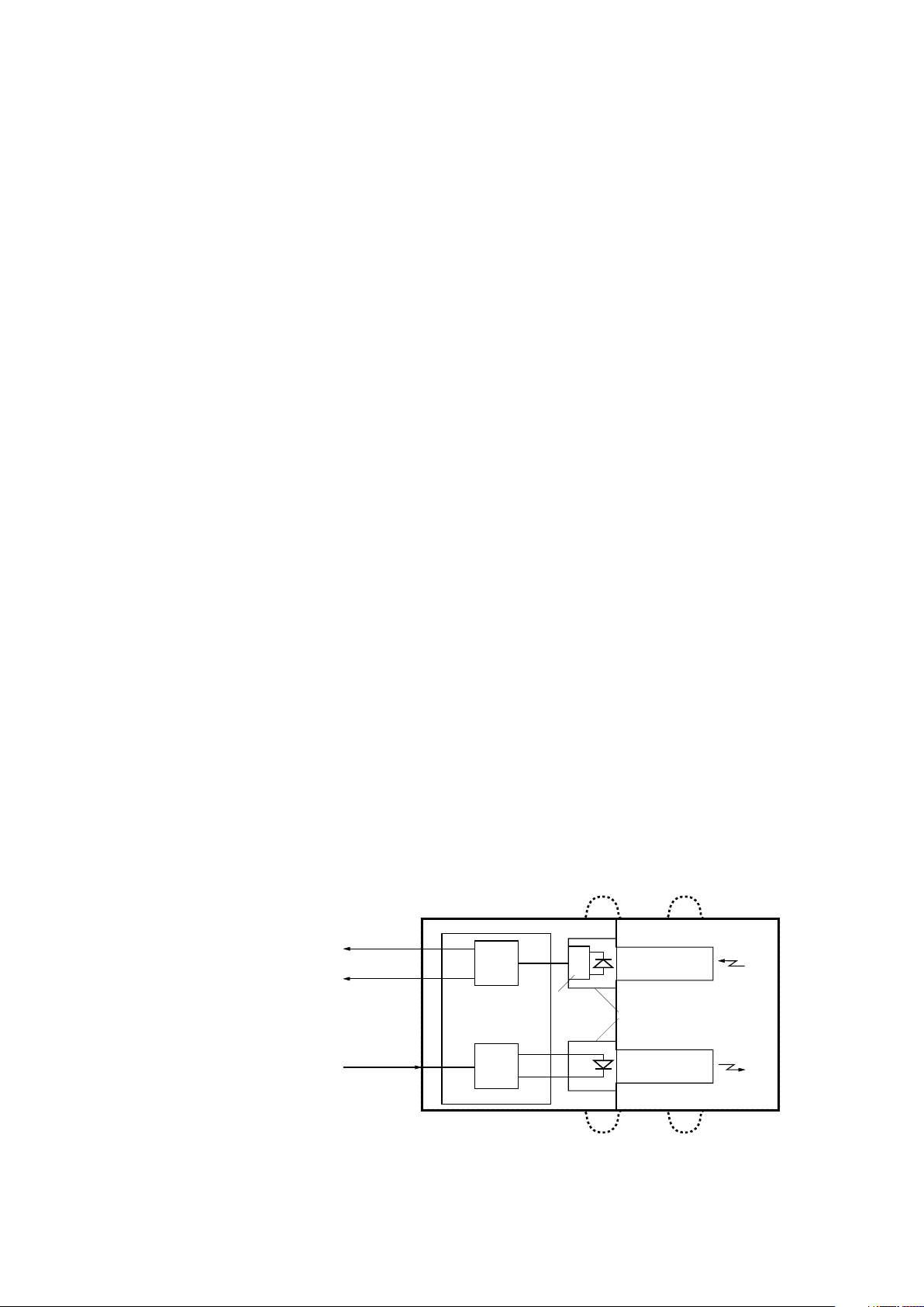
Package
The overall package concept for
the HP transceiver consists of the
following basic elements: two
optical subassemblies, an
electrical subassembly, and the
housing with full compliance to
the FDDI PMD standard. A block
diagram is illustrated in Figure 1.
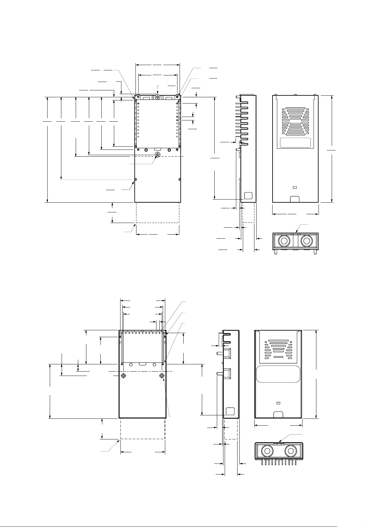
The package outline drawings
and pin-outs are shown in Figures
2 and 3. These are compliant with
the industry standard 2x11 and
1x13 pin configurations.
The optical subassemblies utilize
a high-volume assembly process
together with low-cost lens
elements which result in a cost-
effective building block.
The electrical subassemblies
consist of a high-volume, multi-
layer printed circuit board on
which the IC chips and various
surface-mounted passive circuit
elements are attached.
Each transceiver package
includes internal shields for the
electrical and optical subassem-
blies to ensure low EMI emissions
and high immunity to external
EMI fields.
The outer housings including the
MIC receptacles are molded of
filled non-conductive plastic to
provide mechanical strength and
electrical isolation. The solder
posts of each package design are
isolated from the circuit design of
the transceiver and do not require
connection to a ground plane on
the circuit board.
Each transceiver is attached to its
printed circuit boards with the
2x11 or 1x13 signal pins and the
solder posts which exit the
bottom of the housing. The solder
posts provide the primary
mechanical strength to withstand
the loads imposed on the
transceiver when mating with
MIC-connectored fiber cables.
Application Information
The Applications Engineering
group of the Optical Communica-
tion Division is available to assist
you with the technical under
Figure 1. HFBR-5111/-5112/-5113 Block Diagram.
DATA OUT
SIGNAL
DETECT OUT
DATA IN
ELECTRICAL SUBASSEMBLY
QUANTIZER IC
DRIVER IC
TOP VIEW
PIN PHOTODIODE
OPTICAL
SUBASSEMBLIES
LED
PREAMP
IC
DIFFERENTIAL
DIFFERENTIAL
DIFFERENTIAL
MEDIA INTERFACE CONNECTOR
RECEPTACLE
94
H
39.94
(1.533)
LATCH
POINTS
33.02
(1.300)
MAX.
2.54
(0.100)
TYP.
34.46 (1.357)
29.00 (1.142)
13X ∅
LEADS
0.48
(0.019)
2X ∅
1.00
(0.039)
2X ∅
SOLDER POSTS
1.52
(0.060)
22.86
(0.900)
19.99
(0.787)
24.86
(0.979)
OPTICAL
REFERENCE
PLANE
5.79
(0.228)
9.14
(0.360)
41.30
(1.626)
16.00
(0.630)
MAX.
2X ∅
3.00
(0.118)
PLUG – REF.
66.16
(2.605)
MAX.
35.80
(1.409)
MAX.
2.95
(0.116)
3.68
(0.145)
0.80
(0.031)
11.87
(0.467)
9.40
(0.370)
MAX.
MAX.
FDDI KEY
LOCATION
PART NUMBER
DATE CODE
COUNTRY OF ORIGIN
30.48 (1.200)
ø
NOTES:
1. ALL DIMENSIONS ARE MILLIMETERS OVER INCHES.
2. ALL DIMENSIONS ARE NOMINAL UNLESS OTHERWISE SPECIFIED.
3. THE LEADS ARE TIN-LEAD PLATED PHOSPHOR BRONZE.
4. THE POSTS ARE TIN-LEAD PLATED BRASS.
5. THE HOUSING IS GLASS FIBER FILLED BLACK POLYETHERIMIDE.
6. THE MODULE IS SHOWN WITHOUT THE FIELD KEY INSTALLED.
H
PART NUMBER
DATE CODE
COUNTRY OF ORIGIN
35.80
1.409
MAX.
82.5
3.248
MAX.
2.54
0.100
TYP.
5.08
0.200
78.87
3.105
LATCH
POINTS
2.95
0.116
2.95
0.116
0.85
0.034
11.87
0.467
9.40
0.370
MAX.
MAX.
FDDI KEY
LOCATION
33.02
1.300
MAX.
35.56
1.400
40.64
1.600
44.45
1.750
45.72
1.800
OPTICAL
REFERENCE
PLANE
81.32
3.202
63.5
2.500
1.52
0.060
SQ.2X
16.00
0.630
MAX.
PLUG – REF.
ACCEPTS SELF TAPPING
2X – M2X0.4 SCREW FOR
OPTIONAL MOUNTING
1.91
0.075
MAX.
2.54
0.100
1.22
0.050
X4X
1.52
0.060
3.80
0.150
2X
34.34
1.352
30.48
1.200
ø
1.50
0.060
4X SOLDER POSTS
ø
0.48
0.019
22X LEADS
Figure 2(a). HFBR-5111 Outline Drawing.
Figure 2(b). HFBR-5112 Outline Drawing.
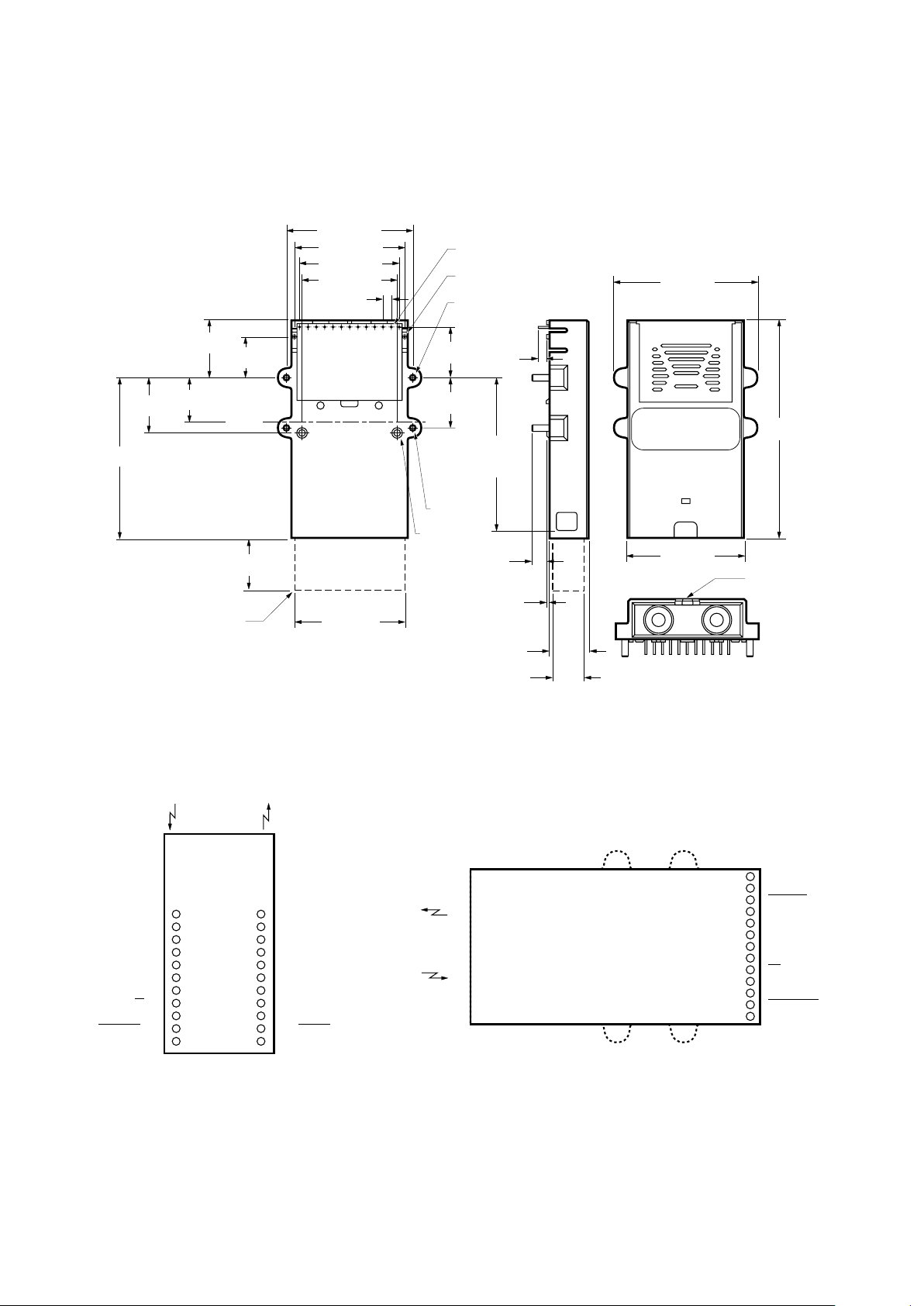
95
Figure 2(c). HFBR-5113 Outline Drawing.
H
46.56
(1.833)
LATCH
POINTS
33.02
(1.300)
MAX.
2.54
(0.100)
TYP.
38.10 (1.500)
34.46 (1.357)
29.00 (1.142)
13X ∅
LEADS
0.48
(0.019)
2X ∅
1.00
(0.039)
4X ∅
SOLDER POSTS
2.00
(0.079)
15.24
(0.600)
15.24
(0.600)
12.37
(0.487)
17.24
(0.679)
OPTICAL
REFERENCE
PLANE
13.41
(0.528)
16.76
(0.660)
48.92
(1.926)
16.00
(0.630)
MAX.
4X R
2.80
(0.110)
2X ∅
3.00
(0.118)
PLUG – REF.
66.16
(2.605)
MAX.
43.80
(1.724)
MAX.
35.80
(1.409)
MAX.
2.95
(0.116)
4.50
(0.177)
0.80
(0.031)
11.87
(0.467)
9.40
(0.370)
MAX.
MAX.
NOTES:
1. ALL DIMENSIONS ARE MILLIMETERS OVER (INCHES).
2. ALL DIMENSIONS ARE NOMINAL UNLESS OTHERWISE SPECIFIED.
3. THE LEADS ARE TIN-LEAD PLATED PHOSPHOR BRONZE.
4. THE POSTS ARE TIN-LEAD PLATED BRASS.
5. THE HOUSING IS GLASS FIBER FILLED BLACK POLYETHERIMIDE.
6. THE MODULE IS SHOWN WITHOUT THE FIELD KEY INSTALLED.
FDDI KEY
LOCATION
PART NUMBER
DATE CODE
COUNTRY OF ORIGIN
30.48 (1.200)
GND 1
NC 2
V
CC
3
V
CC
4
GND 5
GND 6
SD 7
SD 8
V
CC
9
DATA OUT 10
DATA OUT 11
22 GND
21 V
CC
20 V
CC
19 V
CC
18 V
CC
17 GND
16 GND
15 GND
14 V
BB
13 DATA IN
12 DATA IN
TOP VIEW
Figure 3. Pin Assignments.
(a) HFBR-5111
(b) HFBR-5112/-5113
TOP VIEW
GND
V
B
DATA IN
DATA IN
TX V
CC
GND
GND
RX V
CC
SD
SD
DATA OUT
DATA OUT
GND
13
1
96
Hewlett-Packard LED technology
has produced 1300 nm LED
devices with lower aging charac-
teristics than normally associated
with these technologies in the
industry. The industry convention
is 1.5 dB aging for 1300 nm
LEDs, however HP 1300 nm
LEDs will experience less than 1
dB of aging over normal commer-
cial equipment mission life
periods. Contact your Hewlett-
Packard sales representative for
additional details.
Figure 4 was generated with a
Hewlett-Packard fiber-optic link
model containing the current
industry conventions for fiber
cable specifications and the FDDI
PMD optical parameters. These
parameters are reflected in the
guaranteed performance of the
transceiver specifications in this
data sheet. This same model has
been used extensively in the ANSI
and IEEE committees, including
the ANSI X3T9.5 committee, to
establish the optical performance
requirements for various fiber-
optic interface standards. The
cable parameters used come from
the ISO/IEC JTC1/SC 25/WG3
Generic Cabling for Customer
Premises per DIS 11801
document and the EIA/TIA-568-A
Commercial Building Telecom-
munications Cabling Standard per
SP-2840.
Transceiver Signaling
Operating Rate Range and
BER Performance
For purposes of definition, the
symbol rate (Baud), also called
signaling rate, is the reciprocal of
the symbol time. Data rate (bits/
sec) is the symbol rate divided by
the encoding factor used to
encode the data (symbols/bit).
When used in FDDI 100 Mbps
applications, the performance of
the 1300 nm transceivers is
guaranteed over the signaling
rate of 10 MBd to 125 MBd to the
full conditions listed in the
individual product specification
tables.
The transceivers may be used for
other applications at signaling
rates outside of the 10 MBd to
125 MBd range with some
penalty in the link optical power
budget primarily caused by a
reduction of receiver sensitivity.
Figure 5 gives an indication of
the typical performance of these
1300 nm products at different
rates.
These transceivers can also be
used for applications which
require different bit error rate
(BER) performance. Figure 6
illustrates the typical trade-off
between link BER and the
receiver’s input optical power
level.
Figure 5. Transceiver Relative
Optical Power Budget at Constant
BER vs. Signaling Rate.
TRANSCEIVER RELATIVE OPTICAL POWER
BUDGET AT CONSTANT BER – dB
0 200
3.0
0
SIGNAL RATE (MBd)
25 75 100 125
2.5
2.0
1.5
1.0
175
0.5
50 150
CONDITIONS:
1. PRBS 2
7
-1
2. DATA SAMPLED AT CENTER OF DATA SYMBOL.
3. BER = 10
-6
4. T
A
= 25° C
5. V
CC
= 5 V
dc
6. INPUT OPTICAL RISE/FALL TIMES = 1.0/2.1 ns.
standing and design trade-offs
associated with this transceiver.
You can contact them through
your Hewlett-Packard sales
representative.
The following information is
provided to answer some of the
most common questions about
the use of these parts.
Transceiver Optical Power
Budget versus Link Length
The Optical Power Budget (OPB)
is the available optical power for
a fiber-optic link to accommodate
fiber cable losses plus losses due
to in-line connectors, splices,
optical switches, and to provide
margin for link aging and
unplanned losses due to cable
plant reconfiguration or repair.
Figure 4 illustrates the predicted
OPB associated with the trans-
ceivers specified in this data
sheet at the Beginning of Life
(BOL). This curve represents the
attenuation and chromatic plus
modal dispersion losses
associated with the 62.5/125 µm
and 50/125 µm fiber cables only.
The area under the curve
represents the remaining OPB at
any link length, which is available
for overcoming non-fiber cable
related losses.
Figure 4. Optical Power Budget at
BOL vs. Fiber Optic Cable Length.
OPB – OPTICAL POWER BUDGET – dB
0 4.0
14
0
FIBER OPTIC CABLE LENGTH – km
0.5 1.5 2.0 2.5
12
10
8
4
3.5
2
1.0 3.0
6
62.5/125 µm
50/125 µm
 Loading...