


 Loading...
100VG-AnyLAN Multimode
Fiber Transceivers in Low Cost
1x9 Package Style
Technical Data
Features
•Full Compliance with the Optical Performance Requirements of the IEEE 802.12
•Multisourced 1x9 Package Style with Choice of Duplex SC or ST® Receptacles
•Wave Solder and Aqueous Wash Process Compatible
•Manufactured in an ISO 9002 Certified Facility
•820 nm and 1300 nm LED Based Transceivers
Applications
•Multimode Fiber Backbone Links
•Multimode Fiber Wiring Closet to Desktop Links
Description
The HFBR-5106 and HFBR-5107 series transceivers from HewlettPackard provide system designers with products to implement a range of multimode fiber 100VG-AnyLAN physical layer solutions. The transceivers are all supplied in the new industry standard 1x9 SIP package style with a choice of duplex SC or ST® connector interface.
100VG-AnyLAN Backbone
Links
The HFBR-5106/-5106T are 1300 nm products with optical performance compliant with the 100VG-AnyLAN PMD developed by IEEE 802.12. These transceivers are suitable for link lengths up to 2 km.
Alternative 800 nm, Lower Cost 500 m Desktop Links
The HFBR-5107 is a lower cost 800 nm alternative to the HFBR5106 for 100VG-AnyLAN links from the wiring closet to the desktop. It complies with the performance requirements of 802.12 as implemented by Hewlett-Packard at 800 nm wavelength. This transceiver will transfer the full range of 100VG-AnyLan Signals at the required 1x10⁻⁸ Bit Error Rate over distances up to 500 meters using 62.5/125 μm multimode fiber cables. This product is intended for use in cost sensitive applications where the benefits of fiber optic links are important.
Transmitter Sections
The transmitter sections of the HFBR-5106 utilize 1300 nm
HFBR-5106/5106T 1300 nm
HFBR-5107/5107T 820 nm
Surface Emitting InGaAsP LEDs and the HFBR-5107 uses a low cost 820 nm AlGaAs LED. These LEDs are packaged in the optical subassembly portion of the transmitter section. They are driven by a custom silicon IC which converts differential PECL logic signals, ECL referenced (shifted) to a +5 Volt supply, into an analog LED drive current.
Receiver Sections
The receiver section of the HFBR-5106 utilizes InGaAs PIN photodiodes coupled to a custom silicon transimpedance preamplifier IC. The HFBR-5107 series uses the same preamplifier IC in conjunction with an inexpensive silicon PIN photodiode. These are packaged in the optical subassembly portion of the receiver.
150 |
5965-7785E (4/97) |

These PlN/preamplifier combinations are coupled to a custom quantizer IC which provides the final pulse shaping for the logic output and Signal Detect function. The data output is differential. The signal detect output is single-ended. Both data and signal detect outputs are PECL compatible, ECL referenced (shifted) to a +5 Volt power supply.
Package
The overall package concept for the HP transceivers consists of the following basic elements; two optical subassemblies, an electrical subassembly, and the housing with integral duplex SC connector receptacles. This is illustrated in Figure 1.
The package outline and pinout are shown in Figures 2 and 3. The details of this package outline and pinout are compliant with the multisource definition of the 1x9 SIP. The low profile of the HewlettPackard transceiver design complies with the maximum height allowed for the duplex SC connector over the entire length of the package.
The optical subassemblies utilize a high volume process together
with low cost lens elements which result in a cost effective transceiver.
The electrical subassembly consists of a high volume multi-layer printed circuit board on which the IC chips and various surface mount passive circuit elements are attached.
The package includes internal shields for the electrical and optical subassemblies to ensure low EMI and high immunity to electromagnetic fields.
The outer housing, including the duplex SC connector receptacle, is molded of filled non-conductive plastic to provide mechanical strength and electrical isolation. The solder posts of the HewlettPackard design are isolated from the circuit design of the transceiver and do not require connection to a ground plane on the circuit board.
The transceiver is attached to a printed circuit board with the nine signal pins and the two solder posts which exit the bottom of the housing. The two solder posts provide the primary mechanical strength to withstand the loads imposed on the duplex
|
ELECTRICAL SUBASSEMBLY |
DUPLEX SC |
|
DIFFERENTIAL |
|
|
RECEPTACLE |
DATA OUT |
|
|
PIN |
SINGLE-ENDED |
|
|
PHOTODIODE |
SIGNAL |
QUANTIZER IC |
|
|
DETECT OUT |
PREAMP |
|
|
|
|
||
|
|
IC |
OPTICAL |
|
|
|
SUBASSEMBLIES |
DIFFERENTIAL |
|
|
LED |
DATA IN |
|
|
|
|
|
|
|
|
DRIVER IC |
|
|
TOP VIEW
Figure 1. Block Diagram.
or simplex SC connectored fiber cables.
Application Information
The Application Engineering group in the Hewlett-Packard Optical Communications Division is available to assist you with the technical understanding and design trade-offs associated with these transceivers. You can contact them through your Hewlett-Packard sales representative.
The following information is provided to answer some of the most common questions about the use of these parts.
Transceiver Optical
Power
Budget versus Link Length
Optical Power Budget (OPB) is the available optical power for a fiber optic link to accommodate fiber cable losses plus losses due to inline connectors, splices, optical switches, and to provide margin for link aging and unplanned losses due to cable plant reconfiguration or repair.
Figure 4 illustrates the predicted OPB associated with the two transceivers specified in this data sheet at the Beginning of Life (BOL). These curves represent the attenuation and chromatic plus modal dispersion losses associated with the 62.5/125 μm and 50/125 μm fiber cables only. The area under the curve represents the remaining OPB at any link length, which is available for overcoming non-fiber cable related losses.
Hewlett-Packard LED technology has produced 800 nm LED and 1300 nm LED devices with lower aging characteristics than
151

|
ELECTRICAL SUBASSEMBLY |
DUPLEX ST |
|
DIFFERENTIAL |
|
|
RECEPTACLE |
DATA OUT |
|
|
PIN PHOTODIODE |
SINGLE-ENDED |
|
|
|
|
|
|
|
SIGNAL |
QUANTIZER IC |
|
|
DETECT OUT |
PREAMP |
|
|
|
OPTICAL |
||
|
|
IC |
|
|
|
|
SUBASSEMBLIES |
DIFFERENTIAL |
|
|
LED |
DATA IN |
|
|
|
|
|
|
|
|
DRIVER IC |
|
|
|
TOP VIEW |
|
|
Figure 1a. ST Block Diagram.
39.12 |
MAX. |
|
12.70 |
(1.540) |
|
(0.500) |
|
|
|
AREA |
|
25.40 |
|
RESERVED |
12.70 |
|
FOR |
||
(1.000)MAX. |
|
PROCESS |
(0.500) |
|
|
PLUG |
|
HFBR-510X
DATE CODE (YYWW)
COUNTRY OF ORIGIN
|
|
|
|
+ 0.08 |
|
|
10.35 MAX. |
|
|
||||||
|
|
|
0.75 |
|
|
(0.407) |
|
|
|
||||||
|
|
|
|
|
|
|
|
||||||||
3.30 |
± 0.38 |
|
- 0.05 |
|
|
|
|||||||||
|
|
|
|
|
|
|
|
||||||||
|
|
|
|
|
|
|
|||||||||
(0.030 + 0.003 |
) |
|
|
|
|
|
|
||||||||
|
|
|
|
|
|
||||||||||
(0.130 |
± 0.015) |
|
|
|
|
|
|
||||||||
|
- 0.002 |
|
|
|
|
|
|
||||||||
|
|
|
|
|
|
|
|
|
|
|
|
|
|
|
|
|
|
|
|
|
|
|
|
|
|
|
|
|
|
|
|
|
|
|
|
|
|
|
|
|
|
|
|
|
|
|
|
|
|
|
|
|
|
|
|
|
|
|
|
|
|
|
|
|
|
|
|
|
|
|
|
|
|
|
|
|
|
|
|
|
|
|
|
|
|
|
|
|
|
|
|
|
|
|
|
|
|
|
2.92 |
|
18.52 |
+ 0.25 |
|
|
|
|
|
(0.115) |
|
|
|
||
|
|
ø 0.46 |
|
(0.729) |
1.27 - 0.05 |
|
|
|
|
|
(9x) |
|
4.14 |
(0.050 + 0.010) |
|
||
|
|
(0.018) |
|
|
(0.163) |
- 0.002 |
|
|
|
|
NOTE 1 |
|
|
NOTE 1 |
|
|
|
23.55 |
20.32 |
[8x(2.54/.100)] |
16.70 |
|
|
17.32 |
20.32 |
23.32 |
(0.927) |
(0.800) |
(0.657) |
|
|
(0.682) |
(0.800) |
(0.918) |
|
|
|
|
0.87 |
|
|
|
|
|
|
|
|
(0.034) |
23.24 |
15.88 |
|
|
|
|
|
|
|
(0.915) |
(0.625) |
|
|
|
NOTE 1: THE SOLDER POSTS AND ELECTRICAL PINS ARE PHOSPHOR BRONZE WITH TIN LEAD OVER NICKEL PLATING.
DIMENSIONS ARE IN MILLIMETERS (INCHES).
Figure 2. Package Outline Drawing.
152

|
|
|
42 |
MAX. |
|
|
|
(1.654) |
|
|
|
|
24.8 |
5.99 |
|
|
|
(0.976) |
(0.236) |
|
25.4 |
MAX. |
|
|
|
(1.000) |
|
|
|
HFBR--510XT5106T |
|
|
|
|
DATE CODE(YYYWWW) |
|
|
|
|
SINGAPORECOUNTRY OF ORIGIN |
|
|
+ 0.08 |
|
|
|
|
|
|
|
|
|
|
0.5 - 0.05 |
|
|
|
|
(0.020)(+ 0.003 ( |
|
12.0 |
MAX. |
|
- 0.002 |
|
(0.471) |
|
|
|
|
3.2 |
|
|
|
|
(0.126) |
|
|
3.3 ± 0.38 |
|
|
|
|
|
|
|
|
20.32 ± 0.38 |
(0.130) (± 0.015) |
|
|
|
|
|
|
φ 0.46 |
|
(± 0.015) |
|
|
|
φ 2.6 |
|
|
|
(0.022) |
+ 0.25 |
||
|
NOTE 1 |
(0.102) |
||
|
- 0.05 |
|||
|
|
|
|
|
20.32 |
[(8x (2.54/0.100)] |
|
|
(+- 0.0020.010 |
17.4 |
|
20.32 |
||
(0.800) |
(0.685) |
|
||
|
|
(0.800) |
||
22.86 |
21.4 |
|
|
|
(0.900) |
(0.843) |
|
|
|
3.6 |
|
|
(0.142) |
|
|
1.3 |
|
|
(0.051) |
23.38 |
18.62 |
|
||
|
(0.921) |
(0.733) |
12.7
(0.500)
(
NOTE 1: PHOSPHOR BRONZE IS THE BASE MATERIAL FOR THE POSTS & PINS WITH TIN LEAD OVER NICKEL PLATING.
DIMENSIONS IN MILLIMETERS (INCHES).
Figure 2a. ST Package Outline Drawing.
1 = VEE
2 = RD N/C
3 = RD
4 = SD
5 = VCC
6 = VCC
7 = TD
8 = TD
N/C
9 = VEE
TOP VIEW
Figure 3. Pin Out Diagram.
153
normally associated with these technologies in the industry. The Industry convention is 3 dB aging for 800 nm and 1.5 dB for 1300 nm LEDs. The HP LEDs will normally experience less than
1 dB of aging over normal commercial equipment mission life periods. Contact your Hewlett-Packard sales representatives for additional details.
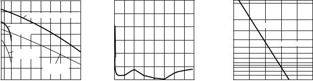
Figure 4 was generated with a Hewlett-Packard fiber optic link module containing the current industry conventions for fiber cable specifications and the 100VG-AnyLAN Optical Parameters. These parameters are reflected in the guaranteed performance of the transceiver specifications in this data sheet. This same model has been used extensively in the ANSI X3T and IEEE committees, including the ANSI X3T12 committee, to establish the optical performance requirements for various fiber optic interface standards. The cable parameters used come from the ISO/IEC JTCI/SC 25/WG3 Generic Cabling for Customer
Premises per DIS 11801 document and the EIA/TIA568-A Commercial Building Telecommunications Cabling Standard per SP-2840.
Transceiver Signaling
Operating Rate Range
and BER Performance
For purposes of definition, the symbol (Baud) rate, also called signaling rate, is the reciprocal of the shortest symbol time. Data rate (bits/sec) is the symbol rate divided by the encoding factor used to encode the data (symbols/bit).
When used in 100VG AnyLAN 100 Mbps applications, the performance of the 1300 nm transceiver is guaranteed over the signaling rate of 10 MBd to
120 MBd to the full conditions listed in the individual product specification tables.
The transceivers may be used for other applications at signaling rates outside of the 10 MBd to 120 MBd range with some penalty in the link optical power
budget primarily caused by a reduction of receiver sensitivity. Figure 5 gives an indication of the typical performance of these 1300 nm products at different rates.
These transceivers can also be used for applications which require different Bit Error Rate (BER) performance. Figure 6 illustrates the typical trade-off between link BER and the receivers input optical power level.
Table 1 lists the hub control signals defined in IEEE 802.12, section 18.5.4.1. These signal rates are below 10 MBd but they are transported with adequate accuracy for hub access control.
Transceiver Jitter
Performance
The Hewlett-Packard 1300 nm transceivers are designed to operate per the system interface jitter specifications listed in Table 27 of section 18.9. of the IEEE 802.12 (100VG-AnyLAN standards).
|
14 |
|
|
|
|
|
|
|
|
BUDGET |
3.0 |
|
|
|
|
|
|
|
|
BUDGETPOWEROPTICAL(dB) |
12 |
|
|
HFBR-5106, 62.5/125 µm |
|
OPTICALRELATIVETRANSCEIVERPOWER |
2.5 |
|
|
|
|
|
|
|
|
||||
|
|
|
|
|
|
|
|
|
|
|
|
||||||||
|
|
|
|
BERCONSTANTAT(dB) |
|
|
|
|
|
|
|
RATEERRORBIT |
|||||||
10 |
HFBR-5107, |
|
|
|
|
|
|
|
|
|
|
|
|
||||||
|
|
|
|
|
|
|
2.0 |
|
|
|
|
|
|
|
|
||||
|
|
|
|
|
|
|
|
|
|
|
|
|
|
|
|
||||
|
8 |
62.5/125 µm |
|
|
|
|
|
|
|
|
|
|
|
|
|
|
|
||
|
|
|
|
|
|
|
|
|
|
|
|
|
|
|
|
|
|
|
|
|
|
|
|
|
|
|
|
|
|
|
1.5 |
|
|
|
|
|
|
|
|
|
6 |
|
|
|
|
|
|
|
|
|
|
|
|
|
|
|
|
|
|
|
|
HFBR-5107, |
|
|
|
|
|
1.0 |
|
|
|
|
|
|
|
|
|||
|
4 |
50/125 µm |
|
|
|
|
|
|
|
|
|
|
|
|
|
|
|||
|
|
|
|
|
|
|
|
|
|
|
|
|
|
|
|
||||
|
2 |
|
|
|
HFBR-5106, |
|
|
0.5 |
|
|
|
|
|
|
|
|
|||
|
|
|
|
50/125 µm |
|
|
|
|
|
|
|
|
|
|
|
|
|||
|
|
|
|
|
|
|
|
|
|
|
|
|
|
|
|
|
|||
|
0 |
|
1.0 |
1.5 |
2.0 |
2.5 |
3.0 |
3.5 |
4.0 |
|
0 |
25 |
50 |
75 |
100 |
125 |
150 |
175 |
200 |
|
0.15 0.5 |
|
0 |
||||||||||||||||
|
|
FIBER OPTIC CABLE LENGTH (km) |
|
|
|
SIGNAL RATE (MBd) |
|
|
|||||||||||
Figure 4. Optical Power Budget at |
CONDITIONS: |
|
1. PRBS 27-1 |
||
BOL vs. Fiber Optic Cable Length. |
2. DATA SAMPLED AT CENTER OF |
|
|
|
DATA SYMBOL. |
|
3. BER = 10-6 |
|
|
4. |
TA = 25° C |
|
5. |
VCC = 5 Vdc |
|
6. |
INPUT OPTICAL RISE/FALL TIMES = 1.0/2.1 ns. |
1 x 10⁻²
1 x 10⁻³
HFBR-510X
1 x 10-4
1 x 10⁻⁵
CENTER OF SYMBOL
1 x 10⁻⁶
1 x 10⁻⁷
1x 10⁻⁸
2.5x 10⁻¹⁰
1 x 10-11
1 x 10-12
-6 |
-4 |
-2 |
0 |
2 |
4 |
RELATIVE INPUT OPTICAL POWER – dB
CONDITIONS:
1.125 MBd
2.PRBS 27-1
3.CENTER OF SYMBOL SAMPLING.
4.TA = 25° C
5.VCC = 5 Vdc
6.INPUT OPTICAL RISE/FALL TIMES = 1.0/2.1 ns.
Figure 5. Transceiver Relative Optical Power Budget at Constant BER vs. Signaling Rate.
Figure 6. Bit Error Rate vs. Relative Receiver Input Optical Power.
154
Loading...