


DVD-3910
Table of contents
 Loading...
For U.S.A., Canada, Europe, Asia,
China,& Japan model
Ver. 6
SERVICE MANUAL
MODEL DVD-
3910
Please refer to the
MODIFICATION NOTICE.
DVD AUDIO-VIDEO / SUPER AUDIO CD PLAYER
注 意
サービスをおこなう前に、このサービスマニュアルを
必ずお読みください。本機は、火災、感電、けがなど
に対する安全性を確保するために、さまざまな配慮を
おこなっており、また法的には「電気用品安全法」に
もとづき、所定の許可を得て製造されております。
従ってサービスをおこなう際は、これらの安全性が維
持されるよう、このサービスマニュアルに記載されて
いる注意事項を必ずお守りください。
●
For purposes of improvement, specifications and
design are subject to change without notice.
●
Please use this service manual with referring to the
operating instructions without fail.
●
Some illustrations using in this service manual are
slightly different from the actual set.
Denon Brand Company, D&M Holdings Inc.
●
●
●
●
TOKYO, JAPAN
本機の仕様は性能改良のため、予告なく変更すること
があります。
補修用性能部品の保有期間は、製造打切後8年です。
修理の際は、必ず取扱説明書を参照の上、作業を行っ
てください。
本文中に使用しているイラストは、説明の都合上現物
と多少異なる場合があります。
X0200V.06 DE/CDM 0707
SAFETY PRECAUTIONS
The following check should be performed for the continued protection of the customer and service technician.
LEAKAGE CURRENT CHECK
Before returning the unit to the customer, make sure you make either (1) a leakage current check or (2) a line to chassis
resistance check. If the leakage current exceeds 0.5 milliamps, or if the resistance from chassis to either side of the power
cord is less than 460 kohms, the unit is defective.
LASER RADIATION
Do not stare into beam or view directly with optical instruments, class 3A laser product.
DVD-3910
CAUTION
Please heed the points listed below during servicing and inspection.
◎ Heed the cautions!
Spots requiring particular attention when servicing, such as
the cabinet, parts, chassis, etc., have cautions indicated on
labels or seals. Be sure to heed these cautions and the cautions indicated in the handling instructions.
◎ Caution concerning electric shock!
(1) An AC voltage is impressed on this set, so touching inter-
nal metal parts when the set is energized could cause
electric shock. Take care to avoid electric shock, by for example using an isolating transformer and gloves when
servicing while the set is energized, unplugging the power
cord when replacing parts, etc.
(2)There are high voltage parts inside. Handle with extra care
when the set is energized.
◎
Caution concerning disassembly and assembly!
Though great care is taken when manufacturing parts from
sheet metal, there may in some rare cases be burrs on the
edges of parts which could cause injury if fingers are moved
across them. Use gloves to protect your hands.
◎ Only use designated parts!
The set's parts have specific safety properties (fire resistance, voltage resistance, etc.). For replacement parts, be
sure to use parts which have the same properties. In particular, for the important safety parts that are marked ! on wiring
diagrams and parts lists, be sure to use the designated parts.
◎ Be sure to mount parts and arrange the
wires as they were originally!
For safety reasons, some parts use tape, tubes or other insulating materials, and some parts are mounted away from the
surface of printed circuit boards. Care is also taken with the
positions of the wires inside and clamps are used to keep
wires away from heating and high voltage parts, so be sure to
set everything back as it was originally.
◎ Inspect for safety after servicing!
Check that all screws, parts and wires removed or disconnected for servicing have been put back in their original positions, inspect that no parts around the area that has been
serviced have been negatively affected, conduct an insulation
check on the external metal connectors and between the
blades of the power plug, and otherwise check that safety is
ensured.
(Insulation check procedure)
Unplug the power cord from the power outlet, disconnect the
antenna, plugs, etc., and turn the power switch on. Using a
500V insulation resistance tester, check that the insulation resistance between the terminals of the power plug and the externally exposed metal parts (antenna terminal, headphones
terminal, microphone terminal, input terminal, etc.) is 1MΩ or
greater. If it is less, the set must be inspected and repaired.
CAUTION
Many of the electric and structural parts used in the set have
special safety properties. In most cases these properties are
difficult to distinguish by sight, and using replacement parts
with higher ratings (rated power and withstand voltage) does
not necessarily guarantee that safety performance will be preserved. Parts with safety properties are indicated as shown
below on the wiring diagrams and parts lists is this service
manual. Be sure to replace them with parts with the designated part number.
(1) Schematic diagrams ... Indicated by the ! mark.
(2) Parts lists ... Indicated by the ! mark.
Concerning important safety parts
Using parts other than the designated parts
could result in electric shock, fires or other
dangerous situations.
注 意
サービス、点検時にはつぎのことにご注意願います。
◎注意事項をお守りください!
サービスのとき特に注意を必要とする個所についてはキャ
ビネット、部品、シャーシなどにラベルや捺印で注意事項を
表示しています。これらの注意書きおよび取扱説明書などの
注意事項を必ずお守りください。
◎感電に注意!
(1) このセットは、交流電圧が印加されていますので通電時
に内部金属部に触れると感電することがあります。従っ
て通電サービス時には、絶縁トランスの使用や手袋の着
用、部品交換には、電源プラグを抜くなどして感電にご
注意ください。
(2) 内部には高電圧の部分がありますので、通電時の取扱に
は十分ご注意ください。
◎分解、組み立て作業時のご注意!
板金部品の端面の『バリ』は、部品製造時に充分管理をして
おりますが、板金端面は鋭利となっている箇所が有りますの
で、部品端面に触れたまま指を動かすとまれに怪我をする場
合がありますので十分注意して作業して下さい。手の保護の
ために手袋を着用してください。
◎指定部品の使用!
セットの部品は難燃性や耐電圧など安全上の特性を持った
ものとなっています。従って交換部品は、使用されていたも
のと同じ特性の部品を使用してください。特に配線図、部品
表に!印で指定されている安全上重要な部品は必ず指定の
ものをご使用ください。
◎部品の取付けや配線の引きまわしは、
元どおりに!
安全上、テープやチューブなどの絶縁材料を使用したり、プ
リント基板から浮かして取付けた部品があります。また内部
配線は引きまわしやクランパーによって発熱部品や高圧部
品に接近しないように配慮されていますので、これらは必ず
元どおりにしてください。
◎サービス後は安全点検を!
サービスのために取り外したねじ、部品、配線などが元どお
りになっているか、またサービスした個所の周辺を劣化させ
てしまったところがないかなどを点検し、外部金属端子部
と、電源プラグの刃の間の絶縁チェックをおこなうなど、安
全性が確保されていることを確認してください。
(絶縁チェックの方法)
電源コンセントから電源プラグを抜き、アンテナやプラグな
どを外し、電源スイッチを入れます。500V 絶縁抵抗計を用
いて、電源プラグのそれぞれの端子と外部露出金属部[アン
テナ端子、ヘッドホン端子マイク端子、入力端子など]との
間で、絶縁抵抗値が1 MΩ 以上であること、この値以下の
ときはセットの点検修理が必要です。
注 意
本機に使用している多くの電気部品、および機構部品は安全
上、特別な特性を持っています。この特性はほとんどの場合、
外観では判別つきにくく、またもとの部品より高い定格(定
格電力、耐圧)を持ったものを使用しても安全性が維持され
るとは、限りません。安全上の特性を持った部品は、この
サービスマニュアルの配線図、部品表につぎのように表示し
ていますので必ず指定されている部品番号のものを使用願
います。
(1) 配線図…!マークで表示しています。
(2) 部品表…!マークで表示しています。
安全上重要な部品について
指定された部品と異なるものを使用した場合に
は、感電、火災などの危険を生じる恐れがあり
ます。
2
DVD-3910
WIRE ARRANGEMENT
If wire bundles are untied or moved to perform adjustment
or parts replacement etc.,be sure to rearrange them neatly
as they were originally bundled or placed afterward.
Otherwise, incorrect arrangement can be a cause of noise
generation.
Wire arrangement viewed from the top
ワイヤー整形図
調整や部品の交換等により、ワイヤー類の結束をはずした
り移動させた場合には、それらの作業が完了した時点でワ
イヤーの整形をおこなってください。正しく整形されてい
ないとノイズ発生の原因となることがあります。
上面からみたワイヤー整形
(Europe model only)
3
3 Deletion of latitude line of weight.
DVD-3910
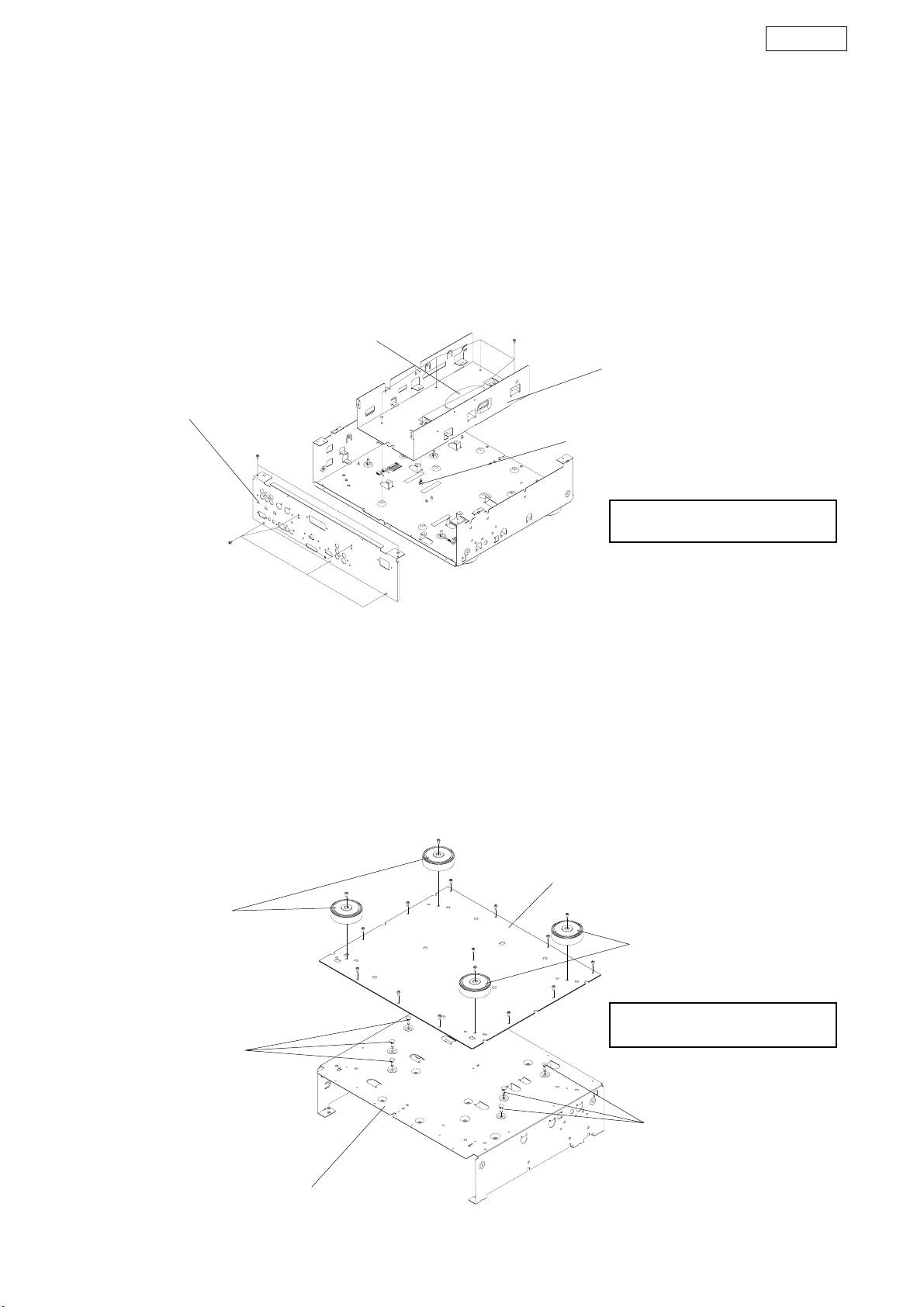
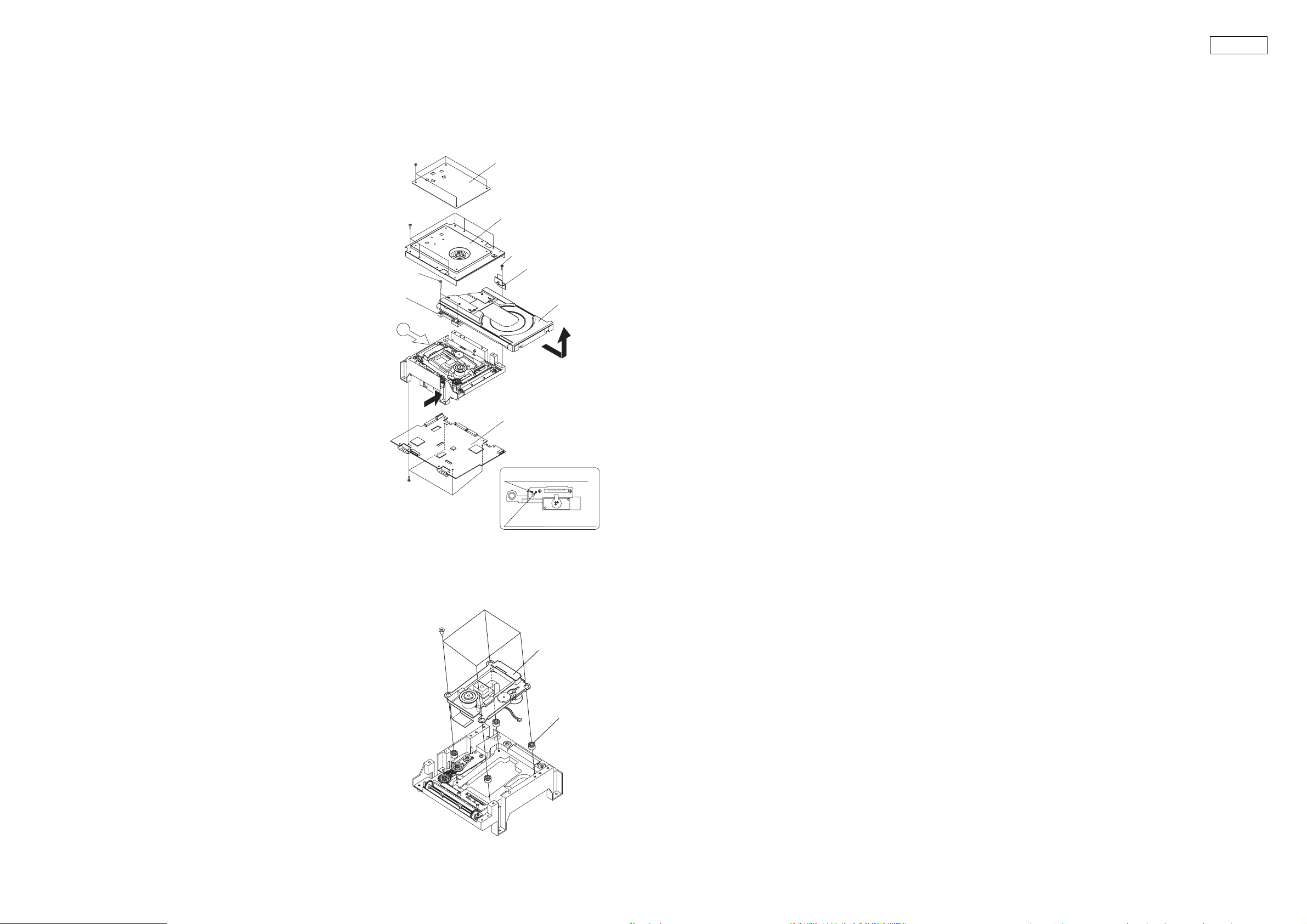
DISASSEMBLY
(Follow the procedure below in reverse order when reas-
各部のはずしかた
(組み立てるときは、逆の順序で行ってください。)
sembling.)
分解と廃棄(Disassembly and abandonment)
(1)Disassembly of a set
It decomposes according to a work procedure1.~11.clause.
(2)Judgment of use parts
It classifies according to the discernment signs in a figure
(c, m, s, p, etc.).
(3)Abandonment of parts
Each part article is discarded according to the specification
abandonment method of each self-governing body.
The parts of ◆ mark show that it shall be remove .
(1)セットの分解
作業手順 1.〜11.項に従い分解を実施します。
(2)使用部品の分別
図中の識別記号(c、m、s、p 等)に従い分別する。
(3)部品の廃棄
各部品は、各自治体の指定廃棄方法に従い廃棄する。
◆記号付き部品は、分離する事。
No. Part Name Q’ty Material No. Part Name Q’ty Material
c · 1䎃
c · 2 DVD mechanism ass’y 1 - m · 2 Front angle 1 SECC
c · 3 Power P.W.B. ass’y 1 - m · 3 Ieee1394 top Shield 1 SPCC
c · 4 Ac inlet 1 - m · 4 Ieee1394 bottom Shield 1 SECC
c · 5 Ferrite core & 3P VH wire 1 - m · 5 Rear panel 1 SECC
c · 6 Video P.W.B. ass’y 1 - m · 6 Mecha base 1 SECC
c · 7 Scart P.W.B. ass’y 1 - m · 7 Bottom cover 1 SECC
c · 8 Audio P.E.B. ass’y 1 - m · 8 Chassis 1 SECC
c · 9 IEEE1394 P.W.B. ass’y 1 - m · 9 Spring 1 SUS304
c · 10 System P.W.B. ass’y 1 - m · 10 Front panel 1 A6063SS
c · 11 D12mm knob ass’y 1 - m (Metals) totals 6,553g
c · 12 Display P.W.B. ass’y 1 -
c · 13 Power-1 P.W.B. ass’y 1 - No. Part Name Q’ty Material
c · 14 Power knob (MAIN) ass’y 1 - s · 1 Screw 3X6 CBTS(S)-B 48 SW
c · 15 Power-2 P.W.B. ass’y 1 - s · 2 Screw 4X8 3P SWELLING 9 SW
c · 16 Power knob (SUB) ass’y 1 - s · 3 Screw 3X8 CBTS(S)-Z 26 SW
c Wire (the othes) 1 - s · 4 Screw 3X8 CBS-Z 2 SW
s · 6 Screw 3X8 FIXING 8 SW
p · 1 P.W.B. support 1 PA66 s · 8 P3 nut for RS-232C 2 SW
p · 2 Foot ass’y 4 ABS s · 9 Screw 3X8 CBTS(P)-B 16 SW
p · 3 P.W.B. spacer 6 PA66 s · 10 Screw 3X10 Special 2 SW
p · 4 Lens 1 PMMA s Washer 2 SPCC/SK
p · 5 Blind ass’y 1 PVC+ s (Screws) totals 81g
p · 6 Inner panel ass’y 1 ABS
p · 7 Part of inner panel 1 ABS Total Weight 9,270g
p · 8 Rubber sheet 2 CR Recycle Weight 6,998g
p · 9 Rubber sheet 1 CR Abandonment Weight 2,272g
The parts of ◆ mark show that it shall be remove at the disassembly and the abandonment
◆ CE04W2G470MC (KMG) ĭ16.0×h31.5mm C-909 c · 3 Power P.W.B. ass’y (GU-3614-2) 1
3
◆ CE04W1A222MC (KY)J30 ĭ10.0×h30.0mm C-918, C-952 c · 3 Power P.W.B. ass’y (GU-3614-2) 2
Loader Panel ass’y 1 - m · 1 Top cover 1 SECC+PVC
c (Complex) totals 2,272g s · 5 Screw 3X8 CFTS(S) 2 SW
No. Part Name Q’ty Material s · 7 P3 nut for DVI 2 SW
p (Plastics) totals 364g
Part Name Dimensions Ref.No. Unit No. Q’ty
4
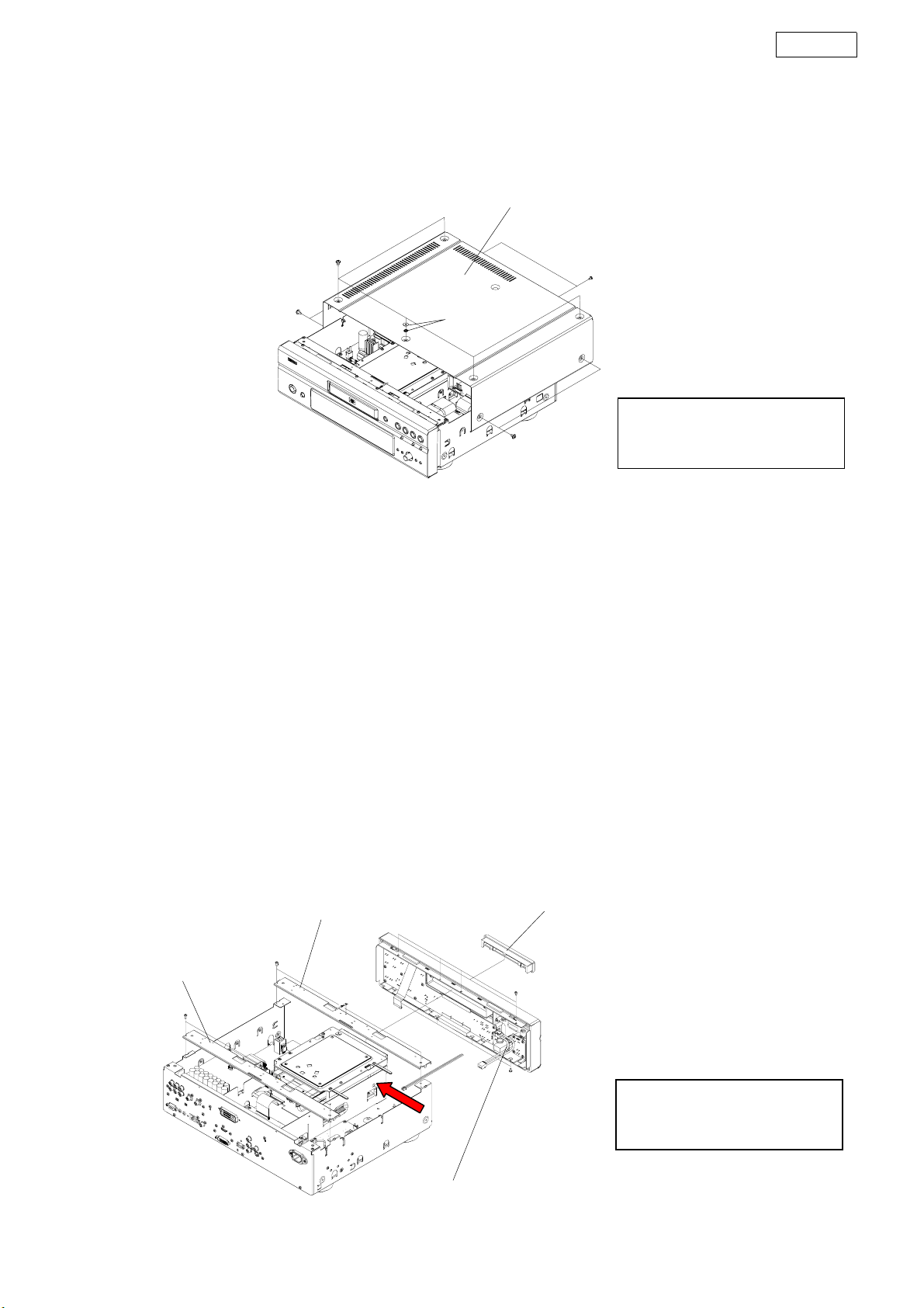
1. Top cover
締結トルク
締結トルク
(1)Remove 2 screws(s ・1) on the rear side and 9
screws(s・2) on the top and the both sides.
Remove 2-washer at the front center on the top.
(2)Widen the Top cover a little laterally, then detach it
with sliding.
s・2
DVD-3910
(1)背面側から s・1のねじ2 本と天・側面から s・2 のねじ 9
本をはずします。天前中央のみワッシャー 2 個共締め。
(2)左右へ少し広げて m・1:Topcover をはずします
m・1:Top cover
㨟㨯1
s・2
2. Front panel sub ass'y & etc.
2-1.When the Disc tray can be ejected electrically.
(1)Switch on , and press 「OPEN/CLOSE」 button to
open the Disc tray.
(2)Detach the Loader panel ass'y by lifting.
(3)Close the Disc tray.
(4)Disconnect the wire [CX031] [CX025] [CY211]
connecting a・1:From the Front panel sub ass’y.
(5)Remove 4 top screws(s・1) and 4 bottom screws
(s・1) , then detach the Front panel sub ass’y .
(6)Remove 2 top screws(s・3) , then detach the m2 :
Front angle. Use 2 pieces of F.Angle for Japan.
2-2.When the Disc tray cannot be ejected
electrically.
(1)Insert a driver into the left 8mm hole , and push
the Plate Gear of the DVD Mechanism , to open the
Disc Tray. (Arrow direction)
(2)The same steps described on 2-1.(2)〜(6).
s:2-washer
s・1:
(Tighten-torque)
s・2
2-1.ディスクトレイが電動でオープン出来る場合
(1)電源を入れ「OPEN/CLOSE」ボタンを押して、ディスクトレイを
開きます。
(2)c・1:Loaderpanelass'y を持ち上げてはずします。
(3)ディスクトレイを閉じます。
(4)a・1:Frontpanelsubass'y からのワイヤー[CX031][CX025]
[CY211] をはずします。
(5)天・底面からs・1のねじ各 4 本をはずし、a・1:Front
panelsubass'y をはずします。
(6)天面からs・3 のねじ 2 本をはずし、m・2:Frontangle
をはずします。国内モデルのみ 2 個使用。
2-2.ディスクトレイが電動でオープン出来ない場合
(1)左側面のΦ8mm 孔よりドライバー等を挿し込みメカユニットの
プレートギアを押してディスクトレイを開きます。(矢印方向)
(2)2-1.(2)〜(6)の作業に同じ。
s・2:締結トルク:1.0Nm
(Tighten-torque)
:0.5Nm
m・2:Front angle
(only Japan)
(only Japan)
s・3
m・2:Front angle
s・3
c・1:Loader panel ass’y
s・1
㨟㨯1
a・1:Front panel sub ass’y
5
s・1:
(Tighten-torque)
s・3:締結トルク:0.5Nm
(Tighten-torque)
:0.5Nm
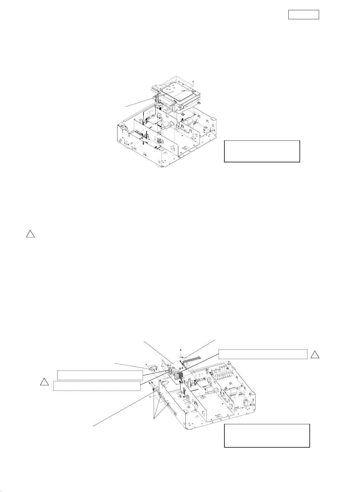
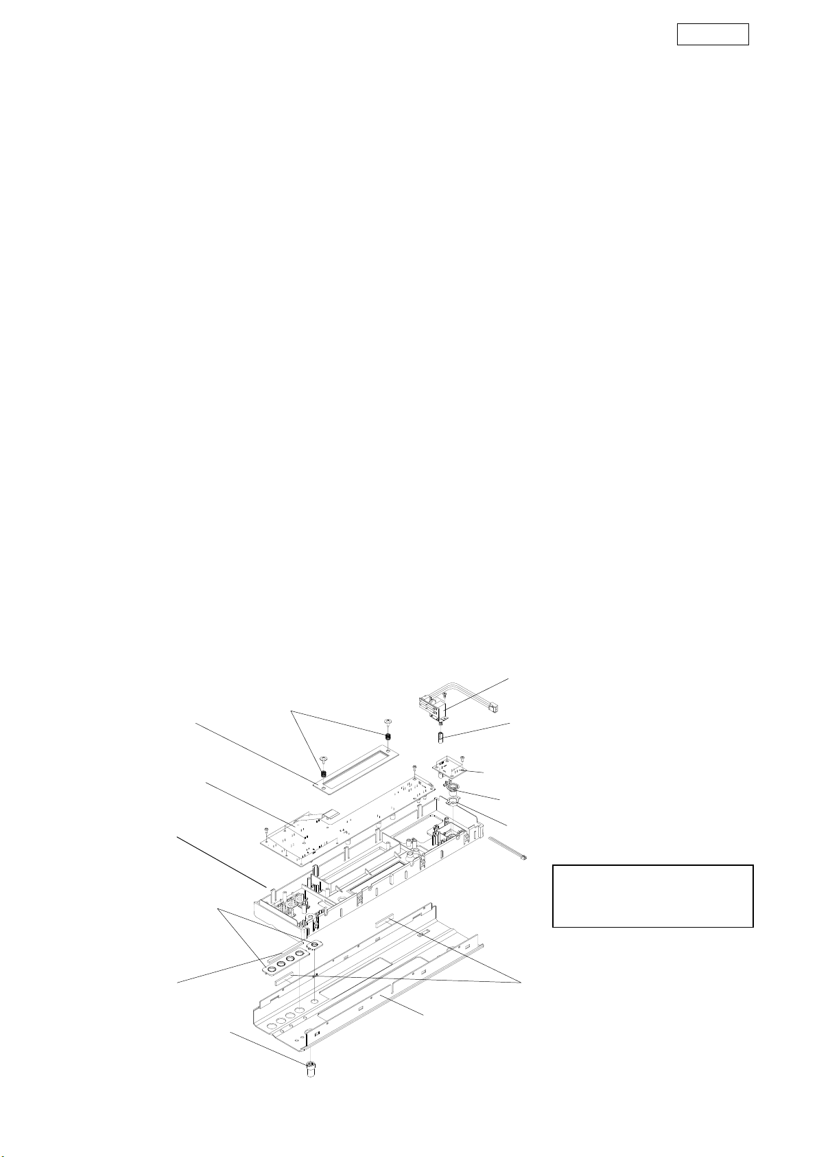
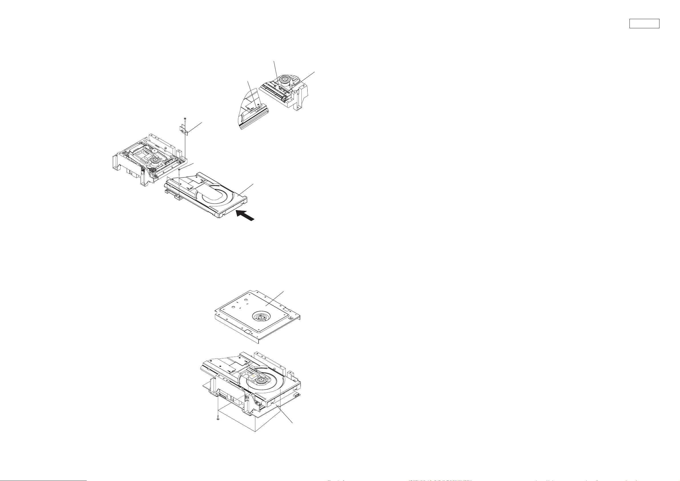
3. DVD mechanism ass'y
y
r
◆
◆
◆
(1)Remove 4 screws (s · 3) on the top side.䎃
(2)Disconnect [CY251] [CY301] [CY171] [CX331]
[CY101] from the MAIN P.W.B. (GU-3618).
(3)Take the DVD mechanism ass'y (s ·2) off.
c · 2㧦DVD mechanism ass'y
4. Power P.W.B. ass'y etc.
4-1.Power P.W.B. ass'y
(1)Remove 2 side screws (s · 4) and 5 top screws
(s · 3). Screw 1P-3P EH CON.CORD together at near
the [CX131] (only JAPAN).
(2)Disconnect the wire [CX131] [CX051] [CX024]
connecting c · 5 : Power P.W.B. ass'y.
(3)Detach the c · 5 : Power P.W.B. ass'y.
33
Thing to do abandonment based on WEEE directive
detaching E-Capacitor of C909, C918, C952 when
abandoning Power P.W.B. ass’y.
4-2.AC INLET
(1)Remove 2 rear screws (s · 5).
(2)Disconnect the STO terminals from c · 4 : Ac inlet.
(3)Detach the c · 4 : Ac inlet.
4-3.Ferrite core & 3P VH wire
(1)Cut 3 clamper on the left side of the chassis.
(2)Detach the c · 5 : Ferrite core & 3P VH wire.
DVD-3910
(1)天面側から s・3 のねじ 4 本をはずします。
(2)メイン基板(GU-3618)よりワイヤー[CY251] [CY301] [CY171]
[CX331][CY101]をはずします。
(3)c・2:DVDmechanismass'y をはずします。
s·3
s · 3:締結トルク:0.5Nm
(Tighten-torque)
4-1.電源基板 ass'y
(1)側面からs・4 のねじ 2 本と天面からs・3 のねじ 5 本
をはずします。日本向けモデルのみ 1P-3P EH ワイヤーが
[CX131]横に共締。
(2)c・5:電源基板ass'y からワイヤー[CX131][CX051][CX024]
をはずします。
(3)c・5:電源基板 ass'y をはずします。
電源基板 ass'y の廃棄時は、C909、C918、C952 電解コン
デンサを取外して WEEE 指令に基づく処理をする事。
4-2.ACINLET
(1)背面からs・5 のねじ 2 本をはずします。
(2)c・4:ACINLET から STO コネクターをはずします。
(3)c・4:ACINLET をはずします。
4-3.フェライトコア&3PVH ワイヤー
(1)シャーシ左側面のクランプバンド 3 箇所をカットします。
(2)c・5:フェライトコアと 3PVH ワイヤーをはずします。
c · 3 : Power P.W.B. ass'
s · 3
c · 4 : Ac inlet
C952:ĭ10×h30.0mm:2200µF /10V
3
C918:ĭ10×h30.0mm㧦2200µF /10V
c · 5 : Ferrite core & 3P VH wire
s · 5
s · 4
clampe
c : 1P-3P EH CON.CORD (only Japan)
C909:ĭ16×h31.5mm㧦47µF/400V
s · 3 ~䎃5 : 締結トルク:0.5Nm䎃
(Tighten-torque)
3
6
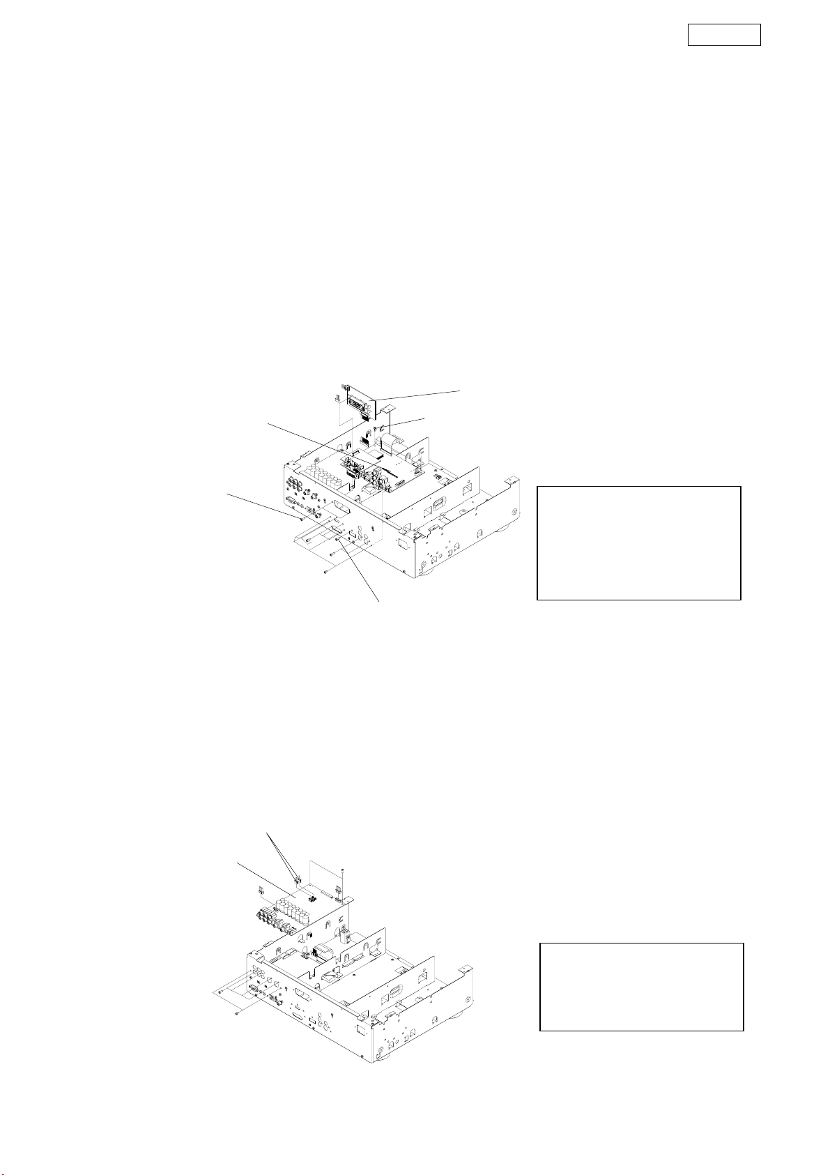
5.Video P.W.B. ass'y and Scart P.W.B. ass'y
y
y
締結トルク
締結トルク
5-1. Video P.W.B. ass'y
(1)Remove 6 screws(s・1) and 2(Japan :3) screws(s・5)
and 2 Nuts(s・6) on the rear side and 2 screws
(s・3) on the top side.
(2)Disconnect [CY174] from the Hdmi P.W.B. ass'y
(GU-3613-3).
(3)Take the Video P.W.B. ass'y(c・6) off.
5-2.Scart P.W.B. ass'y
(1)Remove 2 screws(s・5) on the rear side.
(2)Disconnect [CX053] from the Audio P.W.B. ass'
(GU-3614-1)and [CX121] from the Video P.W.B.
ass'y(GU-3613-2).
(3)Take the Scart P.W.B. ass'y(c・6) off.
DVD-3910
5-1.Video 基板
(1)背面側から s・1 のねじ 6 本と s・5 のねじ 2(国内:3)本と
s・6 のナット 2 本と天面から s・3 のねじ 2 本をはずし
ます。
(2)ビデオ基板 ass'y(GU-3613-3:HDMI 基板 ass'y)より
ワイヤー[CY174] をはずします。
(3)c・6:VideoP.W.B.ass'y をはずします。
5-2.Scart 基板
(1)背面側から s・5 のねじ 2 本をはずします。
(2)オーディオ基板 ass'y(GU-3614-1)よりワイヤー[CX053]を、ビデ
オ基板 ass'y(GU-3613-2)より[CX121]をはずします。
(3)c・7:ScartP.W.B.ass'y をはずします。
c・7:Scart P.W.B. ass'y( only Europe )
c・6:
Video P.W.B. ass'y
s・5( only Europe )
s・6
s・5
s・1
6.Audio P.W.B. ass'y
(1)Remove 2 side screws(s・1) and 4 side screw(s・5)
and 2 top screws(s・3).
(2)Disconnect the wire [CY061][CY072][CY332]
connecting c・8 :Audio P.W.B. ass'y. Disconnect
1P-3P EH CON.CORD from the EH base (onl
JAPAN).
(3)Detach the c・8 : Audio P.W.B. ass'y.
s・3
s・5( only Japan )
(1)背面からs・1 のねじ 2 本とs・5 のねじ 4 本と天面か
(2)c・8:オーディオ基板 ass'y からワイヤー[CY061] [CY072]
(3)c・8:オーディオ基板 ass'y をはずします。
s・1:
(Tighten-torque)
s・3:締結トルク:0.5Nm
(Tighten-torque)
s・5:締結トルク:0.35Nm
(Tighten-torque)
s・6:締結トルク:0.35Nm
(Tighten-torque)
らs・3 のねじ 2 本をはずします。
[CY332]をはずします。国内モデルのみ 1P-3P EH
CON.CORD を EH ベースから外します。
:0.5Nm
c:1P-3P EH CON.CORD (only JAPAN)
c・8:Audio P.W.B. ass'y s・3
s・1
s・5
s・1:
(Tighten-torque)
s・3:締結トルク:0.5Nm
(Tighten-torque)
s・5:締結トルク:0.35Nm
(Tighten-torque)
:0.5Nm
7
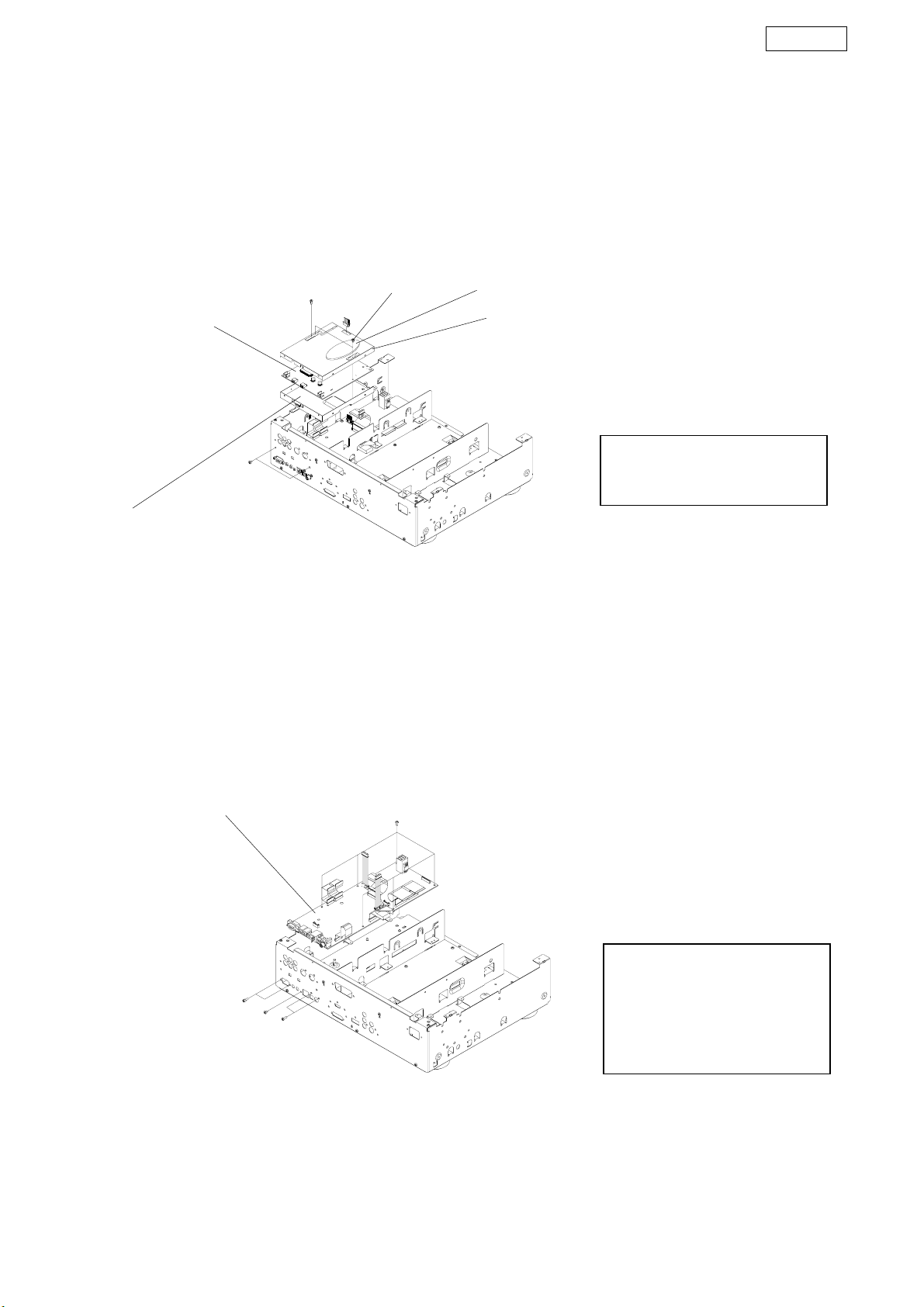
7.IEEE1394 sub ass'y
締結トルク
締結トルク
(1)Remove 2 rear screws(s・1) and 1 top screw(s・3).
(2)Disconnect [CY071] [CY173] [CY191].
(3)Remove 2 top screws(s・1) .
(4)Take the IEEE1394 P.W.B. ass'y(c・9) off.
DVD-3910
(1)背面の s・1 のねじ 2 本と天面の s・3 のねじ 1 本をはず
します。
(2)ワイヤー [CY071][CY173][CY191] をはずします。
(3)天面から s・1 のねじ 2 本をはずします。
(4)c・9:IEEE1394P.W.B.ass'y をはずします。
s・3
c・9:IEEE1394
P. W . B . ass'y
s・1
m・4:Ieee1394 bottom Shield
8.System P.W.B. ass'y
(1)Remove 1 screw(s・1) , 2 screw(s・5) and 2 nuts
(s・6) on the rear and 6 top screws(s・3).
(2)Disconnect [CY131].
(3)Detach the c・10 : System P.W.B. ass'y.
s・1
p:BASS RUBBER(S) (only JAPAN)
m・3:Ieee1394 top Shield
s・1:
(Tighten-torque)
s・3:締結トルク:0.5Nm
(Tighten-torque)
(1)背面からs・1 のねじ 1 本とs・5 のねじ 2 本と s・6 の
ナット 2 本と天面からs・3 のねじ 6 本をはずします。
(2)ワイヤー[CY131] をはずします。
(3)c・10:システム基板 ass'y をはずします。
:0.5Nm
c・10:System P.W.B. ass'y
s・6
s・1
s・5
s・3
s・1:
(Tighten-torque)
s・3:締結トルク:0.5Nm
(Tighten-torque)
s・5:締結トルク:0.35Nm
(Tighten-torque)
s・6:締結トルク:0.35Nm
(Tighten-torque)
:0.5Nm
8
9.Rear panel and Mecha base
締結トルク
締結トルク
9-1.Rear panel
(1)Remove 5 rear screws(s・1) and and 2 top screws
(s・1).
(2)Take the Rear panel(m・5) off.
9-2.Mecha base
(1)Remove 6 screws(s・1) on the top side.
(2)Detach 1 P.W.B. support(p・1) on the bottom.
(3)Take the Mecha base(m・6) off.
p:BASS RUBBER(L) (only JAPAN)
m・5:Rear panel
DVD-3910
9-1.リアパネル
(1)背面側から s・1 のねじ 5 本と天面から s・1 のねじ 2 本
をはずします。
(2)m・5:Rearpanel をはずします。
9-2.メカベース
(1)天面側から s・1 のねじ 6 本をはずします。
(2)底面から P.W.B.サポートをはずします。
(3)m・6:Mechabase をはずします。
s・1
m・6:Mecha base
s・1
s・1
10.Chassis & Bottom cover
10-1.Bottom cover
(1)Remove 4 bottom screws(s・3) from the Foot ass'y.
(2)Take the Foot ass'y(p・2) off.
(3)Remove 12 bottom screws(s・1).
(4)Take the Bottom cover(m・7) off.
10-2.Chassis
(1)Detach 6 P.W.B. spacer (p・3) on the bottom.
(2)Take the Chassis(m・8) off.
s・3
p・2:Foot ass'y
s・3
p・1:P.W.B. support
s・1:
(Tighten-torque)
10-1.ボトムカバー
(1)底面のフット ass'y からs・3 のねじ 4 本をはずします。
(2)p・2:フット ass'y4 個をはずします。
(3)底面からs・1 のねじ 12 本をはずします。
(4)m・7:ボトムカバーをはずします。
10-2.シャーシ
(1)底面から p・3:P.W.B.spacer6 個をはずします。
(2)m・8:シャーシをはずします。
m・7:Bottom cover
s・3
:0.5Nm
p・3:P.W.B. spacer
The others screws:s・1
m・8:Chassis
s・3
9
p・2:Foot ass'y
s・3:
(Tighten-torque)
p・3:P.W.B. spacer
:0.5Nm
11.Parts on Front panel sub ass'y(a.1)
r
締結トルク
y
11- 1.Display P.W.B. ass'y
(1)Remove 7 screws(s・7).
(2)Disconnect [CX052] .
(3)Detach D12mm knob ass'y(c・11).
(4)Take the Display P.W.B. ass'y(c・12) off.
11-2.Power SW-1 P.W.B. ass'y
(1)Remove 2 screws(s・7).
(2)Take the Power SW-1 P.W.B. ass'y(c・13) off.
(3)Take the Power knob(MAIN) ass'y(c・14) off.
11-3.Power SW-2 P.W.B. ass'y
(1)Remove 4 screws(s・7).
(2)Take the Power SW-2 P.W.B. ass'y(c・15) off.
(3)Take the Power knob(SUB) ass'y(c・16) off.
(4)Detach the Lens(p・4).
11-4.Blind ass'y
(1)Remove 2 screws(s・8).
(2)Take the Spring(m・9) and the Blind ass'y(p・5) off.
11-5.Inner panel
(1)Detach 4 top hooks and 4 rear hooks.
(2)Take the Inner panel(p・6) off.
11-6.Front panel
(1)Detach the Part of Inner panel(p ・ 7) and rubbe
sheets(p・8,9) by minus(–) driver or etc..
DVD-3910
11-1.ディスプレイ基板
(1)s・7 のねじ 10 本をはずします。
(2)ワイヤー [CX052] をはずします。
(3)c・11:D12mm ノブ ass'y をはずします。
(4)c・12:ディスプレイ基板をはずします。
11-2.電源 SW-1 基板
(1)s・7 のねじ 2 本をはずします。
(2)c・13:電源 SW-1 基板をはずします。
(3)c・14:電源 MAIN ボタンをはずします。
11-3.電源 SW-2 基板
(1)s・7 のねじ 4 本をはずします。
(2)c・15:電源 SW-2 基板をはずします。
(3)c・16:電源 SUB ボタンをはずします。
(4)p・4:レンズをはずします。
11-4.ブラインド ass'y
(1)s・8 のねじ 2 本をはずします。
(2)m9・:スプリングと p・5:ブラインド ass'y をはずします。
11-5.インナーパネル
(1)上下各 4 個のフックをはずします。
(2)p・6:インナーパネルをはずします。
11-6.フロントパネル
(1)p・7:インナーパネルカット部品や p・8,9:ラバーをマイナスドライバー
等ではずします。
p・5:Blind ass'y
c・11:Display P.W.B. ass'y
p・6:Inner panel
p・7:Part of Inner panel
c・11:D12mm knob ass'y
m・9:Spring
s・7
s・7
s・8
s・7
m・10:Front panel
s・7s・8
c13・:Power-1 P.W.B. ass'y
c・14:Power knob(MAIN) ass'
c15・:Power-2 P.W.B. ass'y
c・16:Power knob(SUB) ass'y
p・4:Lens
s・7:
(Tighten-torque)
s・8:締結トルク:0.35Nm
(Tighten-torque)
p・8:Rubber sheet p・9:Rubber sheet
:0.35Nm
10
DVD-3910
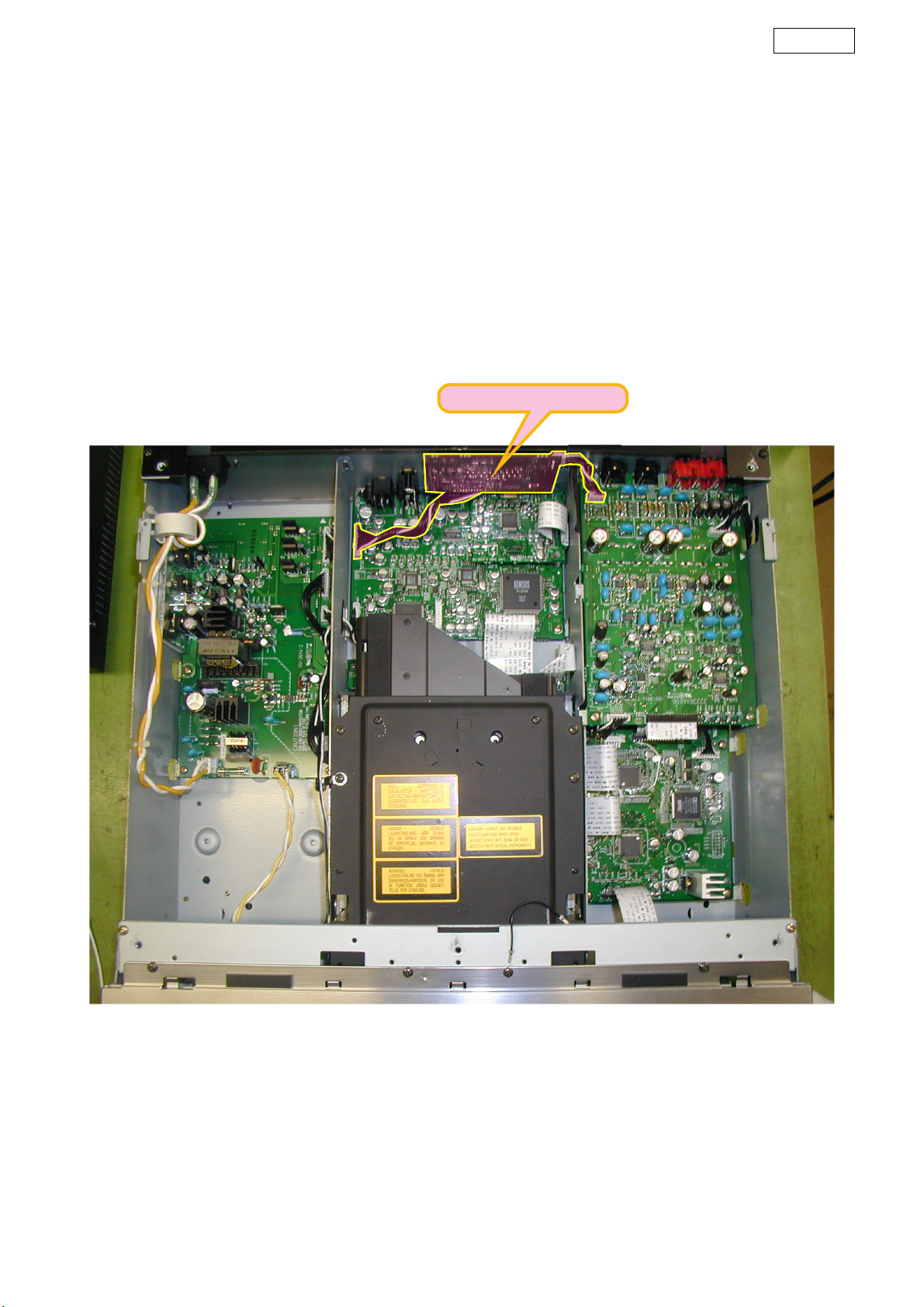
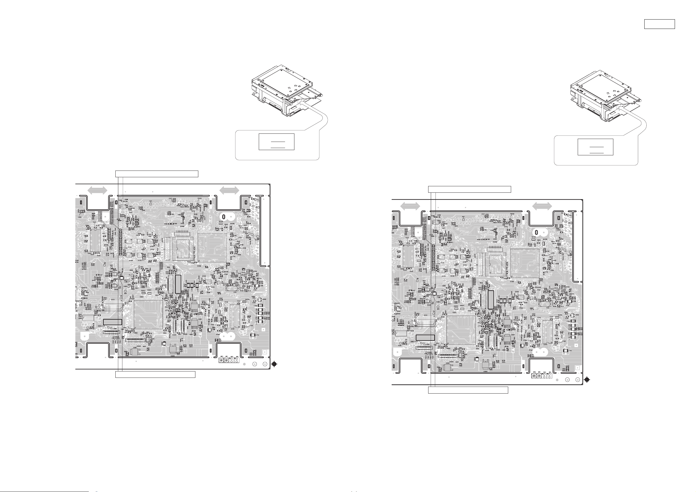
DVD laser drive current measuring points
[DVD] Iop silk point
[CD] Iop silk point
GU-3512 P.W.B. (foil side)
CD laser drive current measuring points
Laser current initial value on the rear of mechanism
DVD
mA
CD
mA
Iop Measurement (Judging for Traverse Unit Replacement)
As to deciding whether optical pickup is defect or not (for replacing traverse unit), follow the steps below.
1. Judging Step
(1) Disc play abnormal
Problems such as disc no read, unsteady playback, etc.
(2) Laser drive current (Iop) check
Check Iop according to the measuring method described in step 2 below.
If the checked value is 1.5 times or more than the initial Iop indicated
on the rear of mechanism unit, the traverse unit should be replaced.
(3) Replacing traverse unit
Referring to “How to Replace Traverse Unit”, replace the traverse unit.
No mechanism adjustment is required as the whole unit is replaced with
a new one.
DVD
CD
Laser current initial value on the rear of mechanism
2. Iop Measuring Method
DVD laser drive current measuring points
[DVD] Iop silk point
mA
mA
ቯ㧔࠻ࡃ࡙ࠬ࠾࠶࠻឵್ቯ㧕
Iop
光ピックアップの故障(トラバースユニットの交換)判定は、下記の手順で行ってください。
判定手順
1.
ディスク再生不具合
(1)
ディスクを読み込まない、スムーズに再生しない等の不具合発生
レーザー駆動電流(
(2)
下記、2項の
メカ背面のレーザー電流初期値の
トラバースユニット交換の目安となります。
トラバースユニット交換
(3)
「トラバースユニットのはずしかた」を参照して、トラバースユ
ニットを交換します。
トラバースユニット単位での交換となりますので、メカ部の調整
は不要です。
の測定方法
2. Iop
Iop
)の確認
Iop
測定方法に従い電流値を確認する。
倍以上になっている場合は、
1.5
CD laser drive current measuring points
[CD] Iop silk point
GU-3512 P.W.B. (foil side)
(1) DVD laser drive current measurement
• Playback the title-1/chapter-1 of DVDT-S01 or commercially available DVD disc.
• Connect an oscilloscope to the test point above and measure the voltage.
• DVD laser drive current is calculated by:
Iop = Measured Voltage Value / 14 (Resistance Value)
(2) CD laser drive current measurement
• Playback the track-1 of TCD-784 or commercially available CD disc.
• Connect an oscilloscope to the test point above and measure the voltage.
• CD laser drive current is calculated by:
Iop = Measured Voltage Value / 12 (Resistance Value)
(1) DVD
(2) CD
レーザー駆動電流の測定
・
DVDT-S01
・上記テストポイントをオシロスコープに接続し、電圧値を測定する。
・
DVD
レーザー駆動電流の測定
・
TCD-784
・上記テストポイントをオシロスコープに接続し、電圧値を測定する。
・CDレーザー駆動電流値 = 「測定した電圧値」/
または市販
レーザー駆動電流値 = 「測定した電圧値」/
または同等市販CDディスクのトラック1を再生する。
ディスクのタイトル1・チャプター1を再生する。
DVD
「14(合成抵抗値)」
「12(合成抵抗値)」
11
DIAGNOSTICS OF OPTICAL PICKUP AND REPLACING TRAVERSE UNIT
1.
శࡇ࠶ࠢࠕ࠶ࡊߩขᛒᵈᗧ
レーザーダイオードの破壊防止。
光素子ユニットを交換するときは、以下を遵守してください。
(1)
光素子ユニットの接続ケーブルをはずすときは、静電対策を行ったデスクの上で作業をしてください。
(2)
作業者はリストストラップを使用してください。
(3)
レーザーダイオードの破壊防止のため、24P
FFC
ケーブルをはずす前にランドを半田付けショートしてください。
(4)
光素子ユニットのコネクタ部に触れないでください。
2.
࠻ࡃ࡙ࠬ࠾࠶࠻ߩ឵
交換時、以下の手順で故障診断をおこなってください。
レーザー駆動電流の現在値が初期値の
150
%以上なら、ピックアップを交換してください。
ピックアップ交換の場合はトラバースユニットを交換し、調整は不要です。初期値はメカ後部のラベルに表示されて
います。
శࡇ࠶ࠢࠕ࠶ࡊขᛒᵈᗧߣ឵
"NO DISC"
␜ޔౣ↢⦟╬
ࠩ㚟േ㔚ᵹ࠴ࠚ࠶ࠢ
HF
ାภ࠴ࠚ࠶ࠢ
࠻ࡃ࡙ࠬ࠾࠶࠻឵
୯㧦ೋᦼ୯ߩ
150%
એ
឵ᓟޔࠩ㚟േ㔚ᵹࠍ࠴ࠚ࠶ࠢߒ߹ߔޕ
୯߇
80mA
એߥࠄᣂࡌ࡞߳ᚻᦠ߈ߒޔ
ᣥࡌ࡞ߩߦ⾍ࠅߟߌ߹ߔޕ
୯߇
80mA
એߥࠄޔౣᐲ࠻ࡃ࡙ࠬ࠾࠶࠻ࠍ឵ߒߡߊߛߐޕ
ޓ
ේ࿃㧦឵ᤨޔ㕒㔚⎕უߐࠇߚޕ
1. Note for Handling the Laser Pick-up
The protection for the damage of laser diode.
If you want to change the optical device unit from any other units, you must keep the following.
(1) It should be done at the desk already took measures the static electricity in care of removing the OPU's
(Optical device unit) connector cable.
(2) Workers should be put on the "Earth Band".
(3) It shold be done to add the solder to the short land to prevent the broken Laser diode before removing the
24P FFC cable.
(4) Don't touch OPU's connector parts carelessly.
2. Optical Pick-up Diagnostics and Replacement
When repairing, carry out failure diagnostics by following the procedure described below.
If the present value of the laser drive current is 150% up to initial value, it is the point of the pickup replacement.
In case of the pickup replacement, replace the Traverse Unit with no adjustment.
The initial value is indicated on the label on back side of Mecha.
NO DISC indicated, Playback not smooth, etc.
DVD-3910
Laser drive current check
HF signal check
Present value: 150% up to initial value
Traverse Unit replacement (refer to page 10)
Laser drive current check after replacement.
If the present value is less than 80mA, write on
the new label by hand, put on the new label over
the old label.
If the present value exceeds 80mA,
replace the Traverse Unit with a new one.
Cause: Damaged electrostatically when replaced.
12
How to Replace Traverse Unit
࠻ࡃ࡙ࠬ࠾࠶࠻ߩ឵ᣇᴺ
1.
࠻ࡃ࡙ࠬ࠾࠶࠻឵Ḱ
(1)
クランプベースダンパーのはずしかた
2.6mm
マシンネジ
(a)4
本をはずして、クランプベー
スダンパーを上へはずします。
(2)
クランプベースのはずしかた
3mmP
タイトネジ
(b)6
本をはずして、クランプベー
スを上へはずします。
(3)
ローダーを開く
メカユニットの左側角孔より、スライダーを定規
やドライバーでトラバース部が下がってローダー
が少し開くまで押します。
(4)
ローダーのはずしかた
・ローダー左のホルダー部より
3mmP
タイトネジ
(c)2
本をはずします。
・ローダー右側より
3mmP
タイトネジ
(d)2
本をはず
し、ベアリングプレートを上へはずします。
・ローダーを前面へ引出し、止まった所で上へは
ずします。
(5)
ピックアップのショート
トラバースユニットのピックアップの静電保護の
為、2ヶ所ショートします。
(ショート箇所は、右図参照)
(6)
メイン基板
ASS'Y
のはずしかた
3mmP
タイトネジ
(e)4
本をはずし、基板を下へはず
します。
2.
࠻ࡃ࡙ࠬ࠾࠶࠻ߩ឵
(1)
トラバースユニットのワイヤーをはずす
・
CX241
:ピック用
24P-FFC
・
CX151
:スピンドル用
15P-FFC
・
CX031:PU
スライド用
3P-PH
ワイヤー
(2)
トラバースユニットをはずす
特殊ネジ
(f)4
本とダンパー4個をはずし、トラバースユ
ニットを上にはずします。
(3)
トラバースユニットの取付
逆の手順で、トラバースユニットを取付けます。
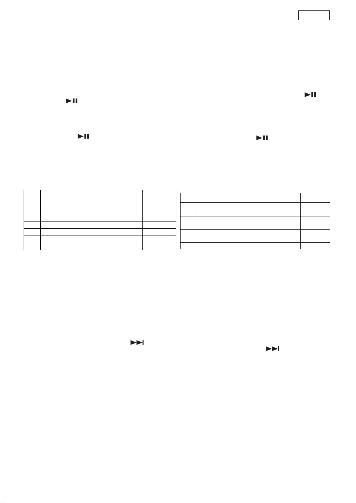
1. Preparing for Replacement
(1) Removing Clamp Base Damper
Remove 4 pcs of 2.6mm machine screw (a), and detach
the Clamp Base Damper upward.
(2) Removing Clamp Base
Remove 6 pcs of 3mm P-tight screw (b), and detach the
Clamp Base upward.
(3) Ejecting Loader
Through the left rectangular hole of the Mechanism Unit,
push the slider with a ruler or driver until the Traverse
portion lowers and the Loader comes out a little.
(4) Removing Loader
• Remove 2 pcs of 3mm P-tight screw (c) on the Loader
Holder left.
• Remove 2 pcs of 3mm P-tight screw (d) on the Loader
Holder right, then pull up the Bearing Plate.
• Fully pull out the Loader forward, and lift up to take it
out.
(5) Shorting Pickup
To protect the Pickup from static electricity, short-circuit
2 positions as shown in figure.
(6) Removing Main P.W.B. Ass'y
Remove 4 pcs of 3mm P-tight screw (e), and detach the
Main P.W.B. Ass'y downward.
(b)
Holder
A
(e)
(c)
(a)
(3)
DVD-3910
Clamp Base Damper
Clamp Base
(d)
Bearing Plate
Loader
(4)
Main P.W.B. Ass'y
Solder to short-circuit (CD)
Solder to short-circuit (CD)
Short-circuit with solder (enlarged fig. A)
(1) Removing Wires
• CX241: 24P-FFC for Pickup
• CX151: 15P-FFC for Spindle
• CX031: 3P-PH wire for PU Slide
(2) Removing Traverse Unit
(3) Mounting Traverse Unit
Remove 4 pcs of special screw (f) and dampers, then
take out the Traverse Unit upward.
Mount the Traverse Unit following the reverse order.
2. Replacing Traverse Unit
(f)
Traverse Unit
Damper
13
3. Installing Loader
4.
⚵┙
(1)
(1)
メイン基板
ASS'Y
の取付
3mmP
タイトネジ
(e)4
本で基板を取付けます。
(2)
ピックアップのショートはずし
ピックアップの
24PFFC
を基板へ接続後、2ヶ所のショー
トをはずします。
(3)
クランプベースの仮置き
レーザーから目を保護する為、クランプベースを仮置き
します。
(4)
トラバースユニットをアップする。
メカユニットの下記ワイヤーを接続し、メカを動作させ
ます。
・
CX141
:電源用の
14P-PH
ワイヤー接続
・
CX131
:ディスプレイ基板からの
13P-FFC
ワイヤー接続
セットの電源を入れ、ローダー開閉ボタンで、
CLOSE
さ
せます。トラバースユニットがアップします。
(
0h00m00s
:表示)
ローダーを前面へ引出し、止まった所で上へはずしま
す。
3.
ࡠ࠳ߩ⚵┙
(1)
ローダーの挿入
ローダーを矢印方向へ止まるまで押しこみます。
ローダを組込時、プレートギアのボスがトレイ裏
面の溝に合う様にプレートギアを右側へ寄せてお
きます。(右図参照)
(2)
ローダーの取付
(c)、(d)
のネジ各2本を取付ます。
(1) Inserting Loader
(2) Fixing Loader
Set and push the Loader to the arrow direction until it
stops. When installing the Loader, move the Plate Gear
to right beforehand so as that the boss of the Plate Gear
fits in the backside groove of the Loader. (See figure right)
Fix the Loader with each 2 screws (c) and (d).
DVD-3910
Plate Gear
Boss
Groove
(d)
Bearing Plate
(c)
Loader
4. Assembly (1)
(1) Assembling Main P.W.B. Ass'y
Fix the Main P.W.B. Ass'y with 4 pcs of 3mm P-tight
screw (e).
(2) Removing Pickup-short Solder
After connecting 24P-FFC of the Pickup with P.W.B.,
remove solder from 2 shorted positions.
(3) Temporary Positioning Clamp Base
To protect your eyes from laser light, put the Clamp Base
temporarily.
(4) Positioning up Traverse Unit
Connect the following wires of the Mechanism Unit, and
operate it.
• CX141: 14P-PH wire for power
• CX131: 13P-FFC wire from Display P.W.B.
Turn on the power to the unit, and press "OPEN/CLOSE"
button to close the Loader.
The Traverse Unit rises up. (display: 0h00m00s)
Pull out the Loader forward, and lift up to take it out.
Clamp Base
(e)
Main P.W.B. Ass'y
14
5.
⚵┙
(2)
(1)
クランプベースダンパーへのアセクロ貼付
クランプベースダンパー裏面の突起3箇所へアセテート
クロステープを貼付します。
(2)
クランプベースの取付
クランプベースダンパーを挿入し、3箇所の突起でクラ
ンパーの位置決めを行います。
3mmP
タイトネジ
(b)6
本
で、クランプベースを取付けます。
6.
⚵┙
(3)
(1)
クランプベースダンパーからアセクロはがし
クランプベースダンパー裏面の突起3箇所からアセテー
トクロステープをはがします。
(2)
クランプダンパーベースの取付
クランプベースダンパーを、クランプベースに先程と
反対向きに挿入します。
3mmS
タイトネジ
(a)4
本で、ク
ランプベースダンパーを取付けます。
5. Assembly (2)
(1) Attaching Tape to Clamp Base Damper
Attach acetate cloth tape to 3 projections of the Clamp
Base Damper backside.
(2) Assembling Clamp Base
Set the Clamp Base Damper with positioning for clamper
by 3 projections.
Fix the Clamp Base with 6 pcs of 3mm P-tight screw (b).
DVD-3910
Acetate Cloth Tape
Clamp Base Damper
Clamp Base Damper
(b)
Clamp Base
6. Assembly (3)
(1) Detaching Tape from Clamp Base Damper
Detach acetate cloth tape from 3 projections of the Clamp
Base Damper backside.
(2) Assembling Clamp Base Damper
Set the Clamp Base Damper to the Clamp Base contrary
to the direction set in step above.
Fix the Clamp Base Damper with 4 pcs of 3mm S-tight
screw (a).
(a)
Clamp Base Damper
15
DVD-3910
SERVICE MODE
1. Aging Mode
(1) preparation
(a) Equipment used: Any one of DVD Karaoke Disc (contain-
ing more than 10 titles).
(b) Unit setting : No spec other than the following procedure
(Aging mode).
At the tray open status, press the “POWER” button to
turn on the power while pressing the “PLAY” and
“OPEN/CLOSE” buttons for DVD operation simulta-
neously. mark on the FL lights, and the unit is set
to the heat run mode.
(2) procedure
(a) According the above, set to the aging mode.
(b) Set a DVD Karaoke disc to the tray and press the “PLAY”
button once. mark on the FL blinks, and aging
operation(after playback title-1 and title-10 of the disc,
the tray open/close is made automatically, then playback
the title-1 again) starts. This aging operation continues
automatically until it is stopped or it stops caused by an
error. In case of some error in DVD, the following error
messages are displayed on the FL.
No Error contents FL display
1 Bad Disc ERROR 02
2 Focus Error ERROR 04
3 Read Error ERROR 03
4 Tracking Error ERROR 04
5Tray Error ERROR 05
6 Navigation Pack Read Error ERROR 06
7 Cmmunication Error ERROR07
サービスモードについて
1.エージングモード
(1) 準備
(a) 使用機器:DVD カラオケディスク(10 タイトル以上
の物)。
(b) 本体設定:下記設定以外規定無。
(エージングモード)
トレイを開けた状態で DVD ユニットの「再生ボタン」
+「開 / 閉ボタン」を同時に押しながら「電源ボタン」
を押してセットの電源を入れると、FL 管の マー
クが点灯し、ヒートランモードに設定される。
(2) 手順
(a) 上記手順でエージングモードに設定する。
(b) トレイに DVD カラオケディスクを入れ、「再生ボタン」
を 1 回押して、FL 管の マークが点滅になると、
「ディスクのタイトル 1 とタイトル 10 を再生した後、
トレイを自動で開 / 閉し、再度タイトル 1 の再生を行
う。」エージング動作になります。停止させるか、エ
ラーにて停止するまでこの動作を自動で繰り返します。
DVD 部にエラーが発生した場合は、FL 管に下表のエ
ラーが表示されます。
No. エラー内容 FL 管表示
1 不良ディスク
2 フォーカスエラー ERROR 04
3 リードエラー
4 トラッキングエラー
5 トレイエラー
6 ナビゲーションパックエラー
7 コマンド通信エラー
ERROR 02
ERROR 03
ERROR 04
ERROR 05
ERROR 06
ERROR 07
2. Initial Setting Mode
(1) Preparation
(a) Equipment used: None
(b) Unit setting: No spec other than the following procedure
(2) Procedure
(a) Initialize the DVD player when µcom, peripheral parts of
µcom, or Main P.W.B. has been replaced in servicing.
(b) Carry out the following to restore factory setting mode. At
the player stop condition, press 3 buttons for DVD oper-
ation(“PLAY”,”OPEN/CLOSE”, and “ SKIP”) until
“INITIALIZE” appears and disappears in the FL.
(“Initialized” appears and disappears on the TV screen.)
(c) All user setting will be lost and its factory setting will be
restored when this initialization is made. Be sure to memorize your setting for restoring again after the initialization.
2.初期設定モード
(1) 準備
(a) 使用機器:無
(b) 本体設定:下記手順以外規定無。
(2) 手順
(a) サービスにて、マイコンやマイコン周辺部分やメイン
基板を交換した場合は、DVD プレーヤーの初期化を
行ってください。
(b) セットの初期化を下記の手順で行い、工場出荷モード
に設定する。
セットが停止状態にて、DVD 操作部の「再生ボタ
ン」+「開 / 閉ボタン」+「 ( スキップ)ボタン」
の 3 重押しを FL 管に "INITIALIZE" が表示され消える
まで押します。(TV 画面には初期化しましたが
表示され消えます。)
(c) 初期化を行うとお客様が設定した内容が工場出荷状態
に戻りますので、あらかじめ設定内容を控えておき初
期化後に再設定してください。
16
DVD-3910
3. μ-Com Firm Check Mode
(1) Preparation
(a) Equipment used: None
(b) Unit setting: No spec other than the following procedure.
(2) Procedure
(a) Press the “POWER” button to turn on the power while
pressing the “PLAY” and “OPEN/CLOSE” buttons for
DVD operation simultaneously.
(b) FL all light mode.
This mode is for detecting FL defects. Press “STILL/
PAUSE ” on the remote control unit once to light
all FL segments.
(c) DVD µcom and main unit µcom firm check mode. This
mode is for displaying the status of each µcom employed.
•DVD µcom firm: Press the 3, 2, 6, 5 buttons on the remote
Then press the “MENU” button or “PUSH ENTER” button.
• Each time the “MENU” button on the remote control
unit or “PUSH ENTER” button is pressed, µcom firm is
displayed one after another.
Ex.: [DRV 6334-1, B/E 030825, SYSTEM 0001, DSP1
6332, DSP2 6333]
Set Serial
No.
(lower 5
digits)
1 00001- 030825 6334 6542 6332 6333
2
3
4
Drive
µcom
B/E
µcom
SYSTEM
µcom
DSP1 DSP2
3.マイコンファームチェックモード
(1) 準備
(a) 使用機器:無
(b) 本体設定:下記手順以外規定無。
(2) 手順
(a) DVD 操作部の「再生ボタン」と「開 / 閉ボタン」を
押しながらセットの「電源ボタン」を押し電源を入れ
ます。
(b) FL 管全点灯モード。
FL 管の故障判別用のモードで、リモコンの「スティ
ル / ポーズ ボタン」を押すと FL 管が全点灯し
ます。
(c) DVD マイコン及び本体マイコンのファーム確認モー
ド
搭載されている各マイコンのファーム状態を表示しま
す。
・ DVD マイコンのファーム:リモコンの「メニューボタ
ン」または、本体の PUSHENTER ボタンを押します。
・ リモコンのメニューボタンまたは、本体の PUSHENTER
ボタンを押すたびにマイコンファームを次々と表示し
ます。
表示例:〔DRV6334-1、B/E030825、SYSTEM0001、Dsp1
6332 、 Dsp26333〕
セットの
シリアル
番号 ( 下 5
桁)
1 00001 〜
2
3
4
ドライブ
マイコン
030825 6334 6542 6332 6333
B/E マイコンシステム
マイコン
Dsp1 Dsp2
17
DVD-3910
4. Setting up the test mode
(1) Setting up ※ Firmware Change needs.
• In order to set up the test mode, you press STOP button
and REV button simultaneously in the heat-run mode.Fundamentaly, you can set up the test mode at the stop state
after disc loading. (Heat-run mode is set up by pressing
PLAY button,holding OPEN/CLOSE button. If it becomes
heat run mode, PLAY indicator and PAUSE indicator will
light up.)
LOADING display
↓
FL display (The display part of 13 digits)
12345678910111213
T
(2) Mode Select
• There are two, servo adjustment value display mode and
trace mode (error rate display), in the mode.
(a) If the REV button or the FWD button is pushed in the test
mode, it will become servo adjustment value display
mode.
FL display (The display part of 13 digits)
12345678910111213
T3
(b) If the REV button or the FWD button is pushed again, it
will become the trace mode (error rate display).
FL display (The display part of 13 digits)
12345678910111213
T7
(3) Mode decision
• The mode will be decided if the PLAY button is pushed in
the state where the mode is chosen.
(a) In the case of servo adjustment value display mode, a
focus offset adjustment value is displayed.
FL display (The display part of 13 digits)
12345678910111213
T31nnnnnnnnnn
(n:adjustment value)
(b) In the case of trace mode (error rate display), trace of
the circumference in one layer is chosen.
FL display (The display part of 13 digits)
12345678910111213
T71FFFFFFFFFF
(F: An address and an error rate display F at the time of undecided.)
(4) Change within the mode
• If the REV button or the FWD button is pushed in the state
where the mode is decided, a change within the mode will
be made.
(a) In the case of servo adjustment value display mode (re-
fer to table 1 servo adjustment value display mode details)
FL display (The display part of 13 digits)
12345678910111213
TXXnnnnnnnnnn
(XX:selection mode [31--62] n:adjustment value)
4. テストモード
(1) テストモードへの投入※ファーム変更が必要です。
・ テストモードへの投入はヒートランモード時に STOP
キーと REV キーを 2 重押しすることで行う。基本的に
ディスクローディング後の停止状態でテストモードに
投入する。( ヒートランモードへの投入は OPEN/CLOSE
キーと PLAY キーを 2 重押しすることで行う。ヒートラ
ンモードになると PLAY インジケータと PAUSE インジ
ケータが点灯する。)
LOADING 表示
↓
FL 管の表示 (13 桁の表示部 )
12345678910111213
T
(2) モードの選択
・ モードには、サーボ調整値表示モードとトレースモード
( エラーレート表示 ) の 2 つがある。
(a) テストモード投入後に REV キー又は FWD キーを押す
と、サーボ調整値表示モードになる。
FL 管の表示 (13 桁の表示部 )
12345678910111213
T3
(b) 再度 REV キー又は FWD キーを押すとトレースモード
( エラーレート表示 ) になる。
FL 管の表示 (13 桁の表示部 )
12345678910111213
T7
(3) モードの確定
・ モードを選択してある状態で PLAY キーを押すとモード
を確定する。
(a) サーボ調整値表示モードの場合は、フォーカスオフ
セット調整値を表示する。
FL 管の表示 (13 桁の表示部 )
12345678910111213
T31nnnnnnnnnn
(n: 調整値 )
(b) トレースモード ( エラーレート表示 ) の場合は、1層
内周のトレースを選択する。
FL 管の表示 (13 桁の表示部 )
12345678910111213
T71FFFFFFFFFF
(F: アドレス及びエラーレートは未確定時、F を表示する。)
(4) モード内での変更
・ モードを確定してある状態で REV キー又は FWD キーを
押すとモード内での変更を行う。
(a) サーボ調整値表示モードの場合(表1サーボ調整値表
示モード詳細参照)
FL 管の表示 (13 桁の表示部 )
12345678910111213
TXXnnnnnnnnnn
(XX: 選択モード [31 〜 62]、n: 調整値 )
18
DVD-3910
(b) In the case of trace mode (error rate display) (refer to ta-
ble 2 trace mode details)
FL display (The display part of 13 digits)
12345678910111213
TYYFFFFFFFFFF
(YY: select mode [71--94] ,F: address and an error rate display F at the
time of undecided)
(5) Execution of trace mode (error rate display)
(refer to table 2 trace mode details)
• Trace will be performed if the PLAY button is pushed after
choosing operation.
FL display (The display part of 13 digits)
12345678910111213
TYYmmmmmmllll
(YY:select mode[71--94],m:address[PBA][HEX],
l:error rate[COUNT/SEC][HEX])
(Note) Renewal of data is carried out for every CD:300 frame and
DVD:85ECC block.
• The mode chosen when selection mode was changed into
the trace execution and the PLAY button was pushed is
performed from the beginning.When the PLAY button is
pushed without changing selection mode, the mode under
selection is performed from the beginning.(If the PLAY
button is pushed, the address corresponding to the chosen mode will be searched again.)
(b) トレースモード ( エラーレート表示 ) の場合(表 2 ト
レースモード詳細参照)
FL 管の表示 (13 桁の表示部 )
12345678910111213
TYYFFFFFFFFFF
(YY: 選択モード [71 〜 94]、F: アドレス及びエラーレートは未確定
時、F を表示する。)
(5) トレースモード ( エラーレート表示 ) の実行(
表 2 トレースモード詳細参照)
・ 動作を選択した後、PLAY キーを押すとトレースを実行
する。
FL 管の表示 (13 桁の表示部 )
12345678910111213
TYYmmmmmmllll
(YY: 選択モード [71 〜 94]、m: アドレス [PBA][HEX]、
l: エラーレート [COUNT/SEC][HEX])
( 注 )CD:300 フレーム ,DVD:85ECC ブロック毎にデータ
更新する。
・ トレース実行中に選択モードを変更し、PLAY キーを押
すと選択したモードを最初から実行する。選択モードを
変更せずに PLAY キーを押した場合も、選択中のモード
を最初から実行する。
(PLAY キーを押したら、選択しているモードに対
応したアドレスを再度サーチする。)
(6) Other operation
(a) If the STOP button is pushed into servo adjustment val-
ue display mode and trace mode (error rate display), it
will return to the state at the time of a test mode injection.
FL display (The display part of 13 digits)
12345678910111213
T
(b) Push the OPEN/CLOSE button twice and carry out ser-
vo readjustment in OPEN operation ->CLOSE operation.
(It readjusts with test mode.)
OPEN display
↓
CLOSE display
↓
LOADING display
↓
FL display (The display part of 13 digits)
12345678910111213
T
(c) By pressing STOP button and REV button simulta-
neously in the test mode, it returns to heat-run mode.
(6) その他の動作
(a) サーボ調整値表示モード、トレースモード ( エラー
レート表示 ) 中に STOP キーを押すとテストモード投
入時の状態に戻る。
FL 管の表示 (13 桁の表示部 )
12345678910111213
T
(b) OPEN/CLOSE キーを 2 回押して、OPEN 動作→ CLOSE
動作で、サーボ再調整する。
( テストモードのまま再調整する。)
OPEN 表示
↓
CLOSE 表示
↓
LOADING 表示
↓
FL 管の表示 (13 桁の表示部 )
12345678910111213
T
(c) テストモード中に STOP キーと REV キーの 2 重押し
( 投入時と同じキー ) で、ヒートランモードに戻る。
19
DVD-3910
(7) Test mode detailed table
Table 1: servo adjustment value display mode details
XX Contents
31 RFPFEOffset layer0 PIofCXD1881ARAnoffset valueand
32 RFP TE Bal
Gain
33 RFPTE Output
Gain
34 RFPTEOffset layer0 TE offset value of CXD1881AR is
35 DSPTEOffset layer0 TE offset value inside CXD1885Q is
36 FcsBias layer0 The focus bias value inside
37 FcsAGC layer0 Theinsidefocusgain(setting0x2000
38 TrkAGC layer0 The inside tracking gain (setting
39 PiOffset layer0 It is the parameter calculated inside
40 FEOffset layer0 It is the parameter calculated inside
41 SEOffset layer0 It is the parameter calculated inside
42 RFPFEOffset layer1 PI ofCXD1881ARAnoffset valueand
Contents
supplementContentsexplanation
FEAnoffsetvalueisdisplayed.
Pioffsetisshowninhigherrank
1Byte.
FEoffsetisshowninlowrank1Byte.
layer0 TEbalancegainvalueofCXD1881AR
layer0 TEoutputgainvalueofCXD1881ARis
isdisplayed.
displayed.
displayed.
displayed.
CXD1885Qisdisplayed.
to 1) value of CXD1885Q is
displayed.。
Therefore,0x1FF2andinthecaseof
0x2012,itisasfollows.
0x1FF2(8178) / 0x2000(8192) =
0.998291015625(fold)
0x2012(8210) / 0x2000(8192) =
1.002197265625(fold)
Notes:Theinsideof()isadecimal
systemequivalent.
0x2000 to 1) value of CXD1885Q is
displayed.。
Therefore,0x1FF2andinthecaseof
0x2012,itisasfollows.
0x1FF2(8178) / 0x2000(8192) =
0.998291015625(fold)
0x2012(8210) / 0x2000(8192) =
1.002197265625(fold)
Notes:Theinsideof()isadecimal
systemequivalent
CXD1885Q.
Thevaluedisplayedonasetservesas
the number of complement of 2 of
2Bytes(es)doubled256.
Avoltagevalueis6.25mVperbit.
CXD1885Q.
Thevaluedisplayedonasetservesas
the number of complement of 2 of
2Bytes(es)doubled256.
Avoltagevalueis6.25mVperbit.
CXD1885Q.
Thevaluedisplayedonasetservesas
the number of complement of 2 of
2Bytes(es)doubled256.
Avoltagevalueis6.25mVperbit.
FEAnoffsetvalueisdisplayed.
Pioffsetisshowninhigherrank
1Byte.
FEoffsetisshowninlowrank1Byte.
(7) テストモード詳細一覧表
表 1サーボ調整値表示モード詳細
XX 内容 内容補足 内容説明
31 RFPFEOffset レイヤ 0 CXD1881AR の PIオフセット値と FE
32 RFP TE Bal
Gain
33 RFPTE Output
Gain
34 RFPTEOffset レイヤ 0 CXD1881AR の TEオフセット値を表
35 DSPTEOffset レイヤ 0 CXD1885Q 内部の TE オフセット値を
36 FcsBias レイヤ 0 CXD1885Q 内部のフォーカスバイア
37 FcsAGC レイヤ 0 CXD1885Q 内 部 フ ォ ー カ スゲイン
38 TrkAGC レイヤ 0 CXD1885Q内部トラッキングゲイン(0
39 PiOffset レイヤ0 CXD1885Q 内部で計算されるパラ
40 FEOffset レイヤ0 CXD1885Q 内部で計算されるパラ
41 SEOffset レイヤ0 CXD1885Q 内部で計算されるパラ
42 RFPFEOffset レイヤ 1 CXD1881AR の PIオフセット値と FE
レイヤ 0 CXD1881ARのTEバランスゲイン値を
レイヤ 0 CXD1881ARのTE出力ゲイン値を表示
オフセット値を表示。
上位 1Byte に Pi オフセットを示す。
下位 1Byte に FEオフセットを示す。
表示す。
す。
示。
表示。
ス値を表示。
(0x2000 を 1 として ) 値を表示。
0x1FF2 や 0x2012 の場合、以下のよ
うになる。
0x1FF2(8178) / 0x2000(8192) =
0.998291015625( 倍 )
0x2012(8210) / 0x2000(8192) =
1.002197265625( 倍 )
注 :() 内は 10 進換算値
x2000 を 1 として ) 値を表示。
0x1FF2 や 0x2012 の場合、以下のよ
うになる。
0x1FF2(8178) / 0x2000(8192) =
0.998291015625( 倍 )
0x2012(8210) / 0x2000(8192) =
1.002197265625( 倍 )
注 :() 内は 10 進換算値
メータ。
セットに表示される値は、256 倍され
た 2Bytes の 2 の補数となる。
電圧値は 1bit あたり 6.25mV。
メータ。
セットに表示される値は、256 倍され
た 2Bytes の 2 の補数となる。
電圧値は 1bit あたり 6.25mV。
メータ。
セットに表示される値は、256 倍され
た 2Bytes の 2 の補数となる。
電圧値は 1bit あたり 6.25mV。
オフセット値を表示。
上位 1Byte に Pi オフセットを示す。
下位 1Byte に FEオフセットを示す。
43 RFP TE Bal
Gain
44 RFPTE Output
Gain
45 RFPTEOffset layer1 TE offset value of CXD1881AR is
46 DSPTEOffset layer1 It is the parameter calculated inside
47 FcsBias layer1 Itistheparametercalculatedinside
layer1 TEbalancegainvalueofCXD1881AR
layer1 TEoutputgainvalueofCXD1881ARis
isdisplayed.
displayed.
displayed.
CXD1885Q.
Thevaluedisplayedonasetservesas
the number of complement of 2 of
2Bytes(es)doubled256.
Avoltagevalueis6.25mVperbit.
CXD1885Q.
Thevaluedisplayedonasetservesas
the number of complement of 2 of
2Bytes(es)doubled256.
Avoltagevalueis6.25mVperbit.
43 RFP TE Bal
Gain
44 RFPTE Output
Gain
45 RFPTEOffset レイヤ 1 CXD1881AR の TEオフセット値を表
46 DSPTEOffset レイヤ 1 CXD1885Q 内部で計算されるパラ
47 FcsBias レイヤ 1 CXD1885Q 内部で計算されるパラ
レイヤ 1 CXD1881ARのTEバランスゲイン値を
レイヤ 1 CXD1881AR の TE出力ゲイン値を表
表示。
示。
示。
メータ。
セットに表示される値は、256 倍され
た 2Bytes の 2 の補数となる。
電圧値は 1bit あたり 6.25mV。
メータ。
セットに表示される値は、256 倍され
た 2Bytes の 2 の補数となる。
電圧値は 1bit あたり 6.25mV。
20
DVD-3910
48 FcsAGC layer1 Theinsidefocusgain(setting0x2000
49 TrkAGC layer1 The inside tracking gain (setting
50 PiOffset layer1 It is the parameter calculated inside
51 FEOffset layer1 It is the parameter calculated inside
52 SEOffset layer1 It is the parameter calculated inside
53 POerror
detection
number
54 POuncorrect-
ableerror
number
55 PIerrordetec-
tionnumber
56 PI uncorrect-
able error
number
57 MirrCount Disc dis-
58 MirrWidth Disc dis-
59 FZCCount Disc dis-
60 PiLevel Disc dis-
61 DiscType DiscType Theyarethecontentsatthetimeof
62 POerror
detection
numberand
address
Errorrate It is invalid at the time of CD
ErrorRate ItisinvalidatthetimeofCD
ErrorRate CD:C1errordetectionnumber
ErrorRate CD:C2uncorrectableerrornumber
criminant
criminant
criminant
criminant
Errorrate PO error detection number is invalid
to1)valueofCXD1885Qisdisplayed.
Therefore,0x1FF2andinthecaseof
0x2012,itisasfollows.
0x1FF2(8178) / 0x2000(8192) =
0.998291015625(fold)
0x2012(8210) / 0x2000(8192) =
1.002197265625(fold)
Notes:Theinsideof()isadecimal
systemequivalent.
0x2000 to 1) value of CXD1885Q is
displayed.
Therefore,0x1FF2andinthecaseof
0x2012,itisasfollows.
0x1FF2(8178) / 0x2000(8192) =
0.998291015625(fold)
0x2012(8210) / 0x2000(8192) =
1.002197265625(fold)
Notes:Theinsideof()isadecimal
systemequivalent
CXD1885Q.
Thevaluedisplayedonasetservesas
the number of complement of 2 of
2Bytes(es)doubled256.
Avoltagevalueis6.25mVperbit.
CXD1885Q.
Thevaluedisplayedonasetservesas
the number of complement of 2 of
2Bytes(es)doubled256.
Avoltagevalueis6.25mVperbit.
CXD1885Q.
Thevaluedisplayedonasetservesas
the number of complement of 2 of
2Bytes(es)doubled256.
Avoltagevalueis6.25mVperbit.
operation.
operation.
Theyarethecontentsatthetimeof
diskdistinction.
Pleasereferto"Table3Disc
distinction information" about the
contentsofavalue.
Theyarethecontentsatthetimeof
diskdistinction.
Pleasereferto"Table3Disc
distinction information" about the
contentsofavalue.
Theyarethecontentsatthetimeof
diskdistinction.
Pleasereferto"Table3Disc
distinction information" about the
contentsofavalue.
Theyarethecontentsatthetimeof
diskdistinction.
Pleasereferto"Table3Disc
distinction information" about the
contentsofavalue.
disktype.
Pleasereferto"Table4Disc
classificationinformation" about the
contentsofavalue.
atthetimeofCDoperation.
48 FcsAGC レイヤ 1 CXD1885Q 内 部 フ ォ ー カ スゲイン
49 TrkAGC レイヤ1 CXD1885Q 内部トラッキングゲイン
50 PiOffset レイヤ1 CXD1885Q 内部で計算されるパラ
51 FEOffset レイヤ1 CXD1885Q 内部で計算されるパラ
52 SEOffset レイヤ1 CXD1885Q 内部で計算されるパラ
53 PO 誤り検出数 エ ラ ー
54 PO 訂正不可数 エ ラ ー
55 PI 誤り検出数 エ ラ ー
56 PI 訂正不可数 エ ラ ー
57 MirrCount ディスク判別ディスク判別時の内容。
58 MirrWidth ディスク判別ディスク判別時の内容。
59 FZCCount デ ィ ス ク判別ディスク判別時の内容。
60 PiLevel ディスク判別ディスク判別時の内容。
61 DiscType ディスク種別ディスク種別の内容。
62 PO 誤り検出数
とアドレス
レート
レート
レート
レート
エラー
レート
(0x2000 を 1 として ) 値を表示。
0x1FF2 や 0x2012 の場合、以下のよ
うになる。
0x1FF2(8178) / 0x2000(8192) =
0.998291015625( 倍 )
0x2012(8210) / 0x2000(8192) =
1.002197265625( 倍 )
注 :() 内は 10 進換算値
(0x2000 を 1 として ) 値を表示。
0x1FF2 や 0x2012 の場合、以下のよ
うになる。
0x1FF2(8178) / 0x2000(8192) =
0.998291015625( 倍 )
0x2012(8210) / 0x2000(8192) =
1.002197265625( 倍 )
注 :() 内は 10 進換算値
メータ。
セットに表示される値は、256 倍され
た 2Bytes の 2 の補数となる。
電圧値は 1bit あたり 6.25mV。
メータ。
セットに表示される値は、256 倍され
た 2Bytes の 2 の補数となる。
電圧値は 1bit あたり 6.25mV。
メータ。
セットに表示される値は、256 倍され
た 2Bytes の 2 の補数となる。
電圧値は 1bit あたり 6.25mV。
CD 時は無効。
CD 時は無効。
CD 時は C1 誤り検出数。
CD 時は C2 訂正不可数。
値の内容は「表3ディスク判別情報」
を参照。
値の内容は「表3ディスク判別情報」
参照。
値の内容は「表3ディスク判別情報」
参照。
値の内容は「表3ディスク判別情報」
参照。
値の内容は「表4ディスク種別情報」
参照。
CD 時は PO 誤り検出数は無効。
21
DVD-3910
Table 2:tracemode details
YY Contents Contentssupplement
71 A display of PO error detection
number of the inner circumferenceof1-layerandanaddress.
72 A display of PO uncorrectable
number of the inner circumferenceof1-layerandanaddress.
73 A display of PI error detection
number of the inner circumferenceof1-layerandanaddress.
74 A display of PI uncorrectable
number of the inner circumferenceof1-layerandanaddress.
75 A display of PO error detection
numberofthecentralcircumferenceof1-layerandanaddress.
76 A display of PO uncorrectable
numberofthecentralcircumferenceof1-layerandanaddress.
77 A display of PI error detection
numberofthecentralcircumferenceof1-layerandanaddress.
78 A display of PI uncorrectable
numberofthecentralcircumferenceof1-layerandanaddress.
79 A display of PO error detection
number of the outer circumferenceof1-layerandanaddress.
80 A display of PO uncorrectable
number of the outer circumferenceof1-layerandanaddress.
81 A display of PI error detection
number of the outer circumferenceof1-layerandanaddress.
82 A display of PI uncorrectable
number of the outer circumferenceof1-layerandanaddress.
83 A display of PO error detection
number of the inner circumferenceof2-layerandanaddress.
84 A display of PO uncorrectable
number of the inner circumferenceof2-layerandanaddress.
85 A display of PI error detection
number of the inner circumferenceof2-layerandanaddress.
86 A display of PI uncorrectable
number of the inner circumferenceof2-layerandanaddress.
87 A display of PO error detection
numberofthecentralcircumferenceof2-layerandanaddress.
88 A display of PO uncorrectable
numberofthecentralcircumferenceof2-layerandanaddress.
89 A display of PI error detection
numberofthecentralcircumferenceof2-layerandanaddress.
90 A display of PI uncorrectable
numberofthecentralcircumferenceof2-layerandanaddress.
91 A display of PO error detection
number of the outer circumferenceof2-layerandanaddress.
92 A display of PO uncorrectable
number of the outer circumferenceof2-layerandanaddress.
93 A display of PI error detection
number of the outer circumferenceof2-layerandanaddress.
94 A display of PI uncorrectable
number of the outer circumferenceof2-layerandanaddress.
ItisinvalidatthetimeofCD
operation.
ItisinvalidatthetimeofCD
operation.
CD:C1errordetectionnumber
CD : C2 uncorrectable error
number
ItisinvalidatthetimeofCD
operation.
ItisinvalidatthetimeofCD
operation.
CD:C1errordetectionnumber
CD : C2 uncorrectable error
number
ItisinvalidatthetimeofCD
operation.
ItisinvalidatthetimeofCD
operation.
CD:C1errordetectionnumber
CD : C2 uncorrectable error
number
Inthecaseof1-layerdisc,itis
invalid.
Inthecaseof1-layerdisc,itis
invalid.
Inthecaseof1-layerdisc,itis
invalid.
Inthecaseof1-layerdisc,itis
invalid.
Inthecaseof1-layerdisc,itis
invalid.
Inthecaseof1-layerdisc,itis
invalid.
Inthecaseof1-layerdisc,itis
invalid.
Inthecaseof1-layerdisc,itis
invalid.
Inthecaseof1-layerdisc,itis
invalid.
Inthecaseof1-layerdisc,itis
invalid.
Inthecaseof1-layerdisc,itis
invalid.
Inthecaseof1-layerdisc,itis
invalid.
表 2トレースモード詳細
YY 内容 補足説明
71 1 層内周の PO 誤り検出数とアド
レスの表示
72 1 層内周の PO 訂正不可数とアド
レスの表示
73 1層内周のPI誤り検出数とアドレ
スの表示
74 1層内周のPI訂正不可数とアドレ
スの表示
75 1 層中周の PO 誤り検出数とアド
レスの表示
76 1 層中周の PO 訂正不可数とアド
レスの表示
77 1層中周のPI誤り検出数とアドレ
スの表示
78 1層中周のPI訂正不可数とアドレ
スの表示
79 1 層外周の PO 誤り検出数とアド
レスの表示
80 1 層外周の PO 訂正不可数とアド
レスの表示
81 1層外周のPI誤り検出数とアドレ
スの表示
82 1層外周のPI訂正不可数とアドレ
スの表示
83 2 層内周の PO 誤り検出数とアド
レスの表示
84 2 層内周の PO 訂正不可数とアド
レスの表示
85 2層内周のPI誤り検出数とアドレ
スの表示
86 2層内周のPI訂正不可数とアドレ
スの表示
87 2 層中周の PO 誤り検出数とアド
レスの表示
88 2 層中周の PO 訂正不可数とアド
レスの表示
89 2層中周のPI誤り検出数とアドレ
スの表示
90 2層中周のPI訂正不可数とアドレ
スの表示
91 2 層外周の PO 誤り検出数とアド
レスの表示
92 2 層外周の PO 訂正不可数とアド
レスの表示
93 2層外周のPI誤り検出数とアドレ
スの表示
94 2層外周のPI訂正不可数とアドレ
スの表示
CD 時は無効。
CD 時は無効。
CD 時は C1 誤り検出数。
CD 時は C2 訂正不可数。
CD 時は無効。
CD 時は無効。
CD 時は C1 誤り検出数。
CD 時は C2 訂正不可数。
CD 時は無効。
CD 時は無効。
CD 時は C1 誤り検出数。
CD 時は C2 訂正不可数。
1 層ディスクの場合、無効。
1 層ディスクの場合、無効。
1 層ディスクの場合、無効。
1 層ディスクの場合、無効。
1 層ディスクの場合、無効。
1 層ディスクの場合、無効。
1 層ディスクの場合、無効。
1 層ディスクの場合、無効。
1 層ディスクの場合、無効。
1 層ディスクの場合、無効。
1 層ディスクの場合、無効。
1 層ディスクの場合、無効。
22
DVD-3910
Table 3:Discdistinctioninformation
MirrCount MirrWidth FZCCountPILevel
NoDisc Except2
CDHigh
reflection
CDLow
reflection
DVDHigh
reflection
DVDLow
reflection
DVD2-layer 2 Lessthan
SACDHybrid 3 - - -
and3
2Morethan
2Morethan
2 Lessthan
2 Lessthan
---
0x8ED
0x8ED
0x8ED
0x8ED
0x8ED
-Morethan
-Lessthan
1Morethan
1Lessthan
2-
0x99
0x98
0x81
0x80
PIlevelFormula:PIlevel(V)=Measuredvalue × 1.6 ÷ 256
"-":Invalid
Table 4:Discclassificationinformation
DiscType Media
0x00 NoDisc
0x01 UnknownDisc
0x04 DVDSingleLowreflection
0x05 DVDDualParallelLowreflection
0x06 DVDDualOppositeLowreflection
0x08 CDDALowreflection
0x0A VCDLowreflection
0x44 DVDSingleHighreflection
0x48 CDDAHighreflection
0x4A VCDHighreflection
0x8F SACDHybridDisc
表3ディスク判別情報
MirrCount MirrWidth FZCCountPILevel
NoDisc 2 と 3 以外 - - CD 高反射 2 0x8ED 以上 - 0x99 以上
CD 低反射 2 0x8ED 以上 - 0x98 以下
DVD 高反射 2 0x8ED 以下 1 0x81 以上
DVD 低反射 2 0x8ED 以下 1 0x80 以下
DVD2 層 2 0x8ED 以下 2 SACDHybrid 3 - - -
PIlevel計算式:PIlevel(V)=測定値× 1.6 ÷ 256
"-" は無効
表4ディスク種別情報
DiscType Media
0x00 NoDisc
0x01 UnknownDisc
0x04 DVDSingle低反射
0x05 DVDDualParallel低反射
0x06 DVDDualOpposite低反射
0x08 CDDA低反射
0x0A VCD低反射
0x44 DVDSingle高反射
0x48 CDDA高反射
0x4A VCD高反射
0x8F SACDHybridDisc
23
DVD-3910
トラブ
グ
管点灯せず
立ち上がりチェック工程
電源電圧確認
半田付けを確認
発振波形確認
半田付けを確認
電源電圧確認
半田付けを確認
信号の確認
半田付けを確認
データバスの確認
半田付けを確認
不良
次のステップ
立ち上げチェック工程
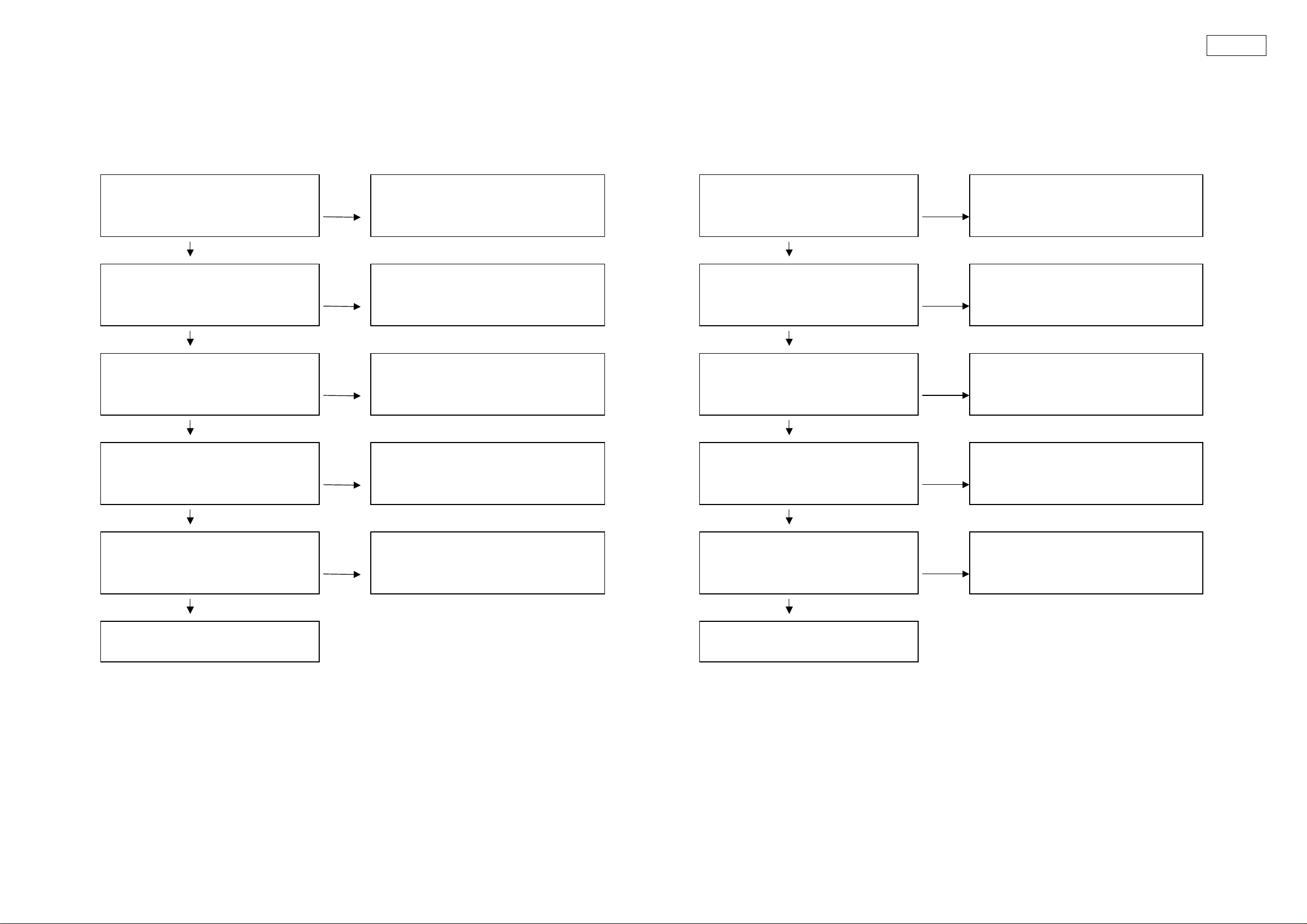
TROUBLE SHOOTING
ルシューティン
1. GU-3618 (MAIN UNIT) ,GU-3613-1 (SYSTEM UNIT) 1. GU-3618 (MAIN UNIT) ,GU-3613-1 (SYSTEM UNIT)
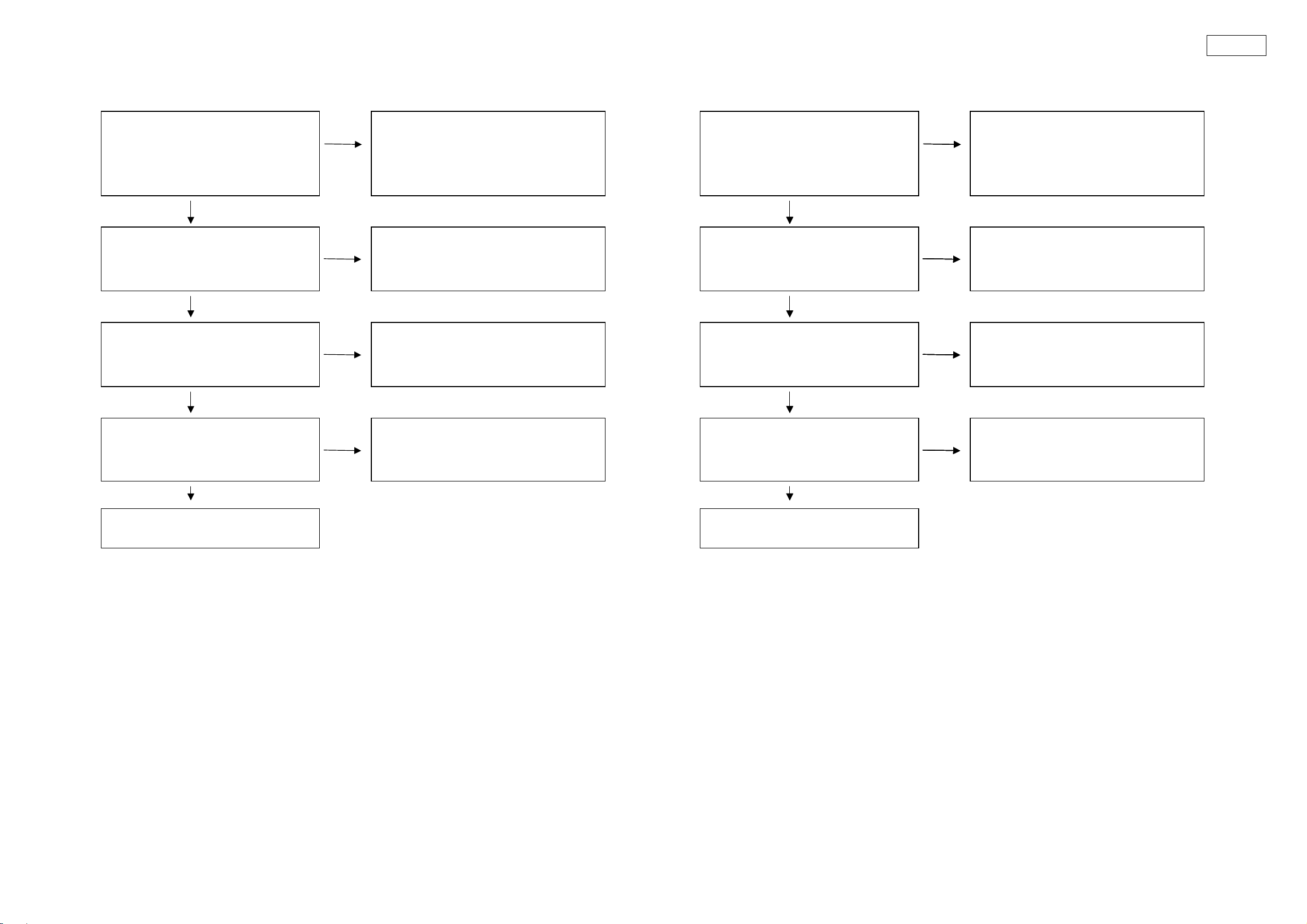
1.1. FL TUBE dosen't light 1.1. FL
(1) Check the Set-up process of System 㱘-COM (1)システムµ-COM
Check Power Supply Voltages.
GU-3613-1(SYSTEM UNIT) GU-3613-1(SYSTEM PWB)
・ [IC202]:D1,D4 N.G Check Soldering. ・ [IC202]:D1,D4 N.G
+3.3V_D1,+3.3V_D4 ・ CY131 on SYSTEM UNIT. +3.3V_D1,+3.3V_D4 ・ SYSTEM UNITのCY131
O.K. O.K.
Check Oscillation waveform.
GU-3613-1(SYSTEM UNIT) GU-3613-1(SYSTEM UNIT)
・ [IC202]: N.G Check Soldering. ・ [IC202]: N.G
16MHz at 13pin. ・ X201 on SYSTEM UNIT. 16MHz at 13pin. ・ SYSTEM UNITのX201
O.K. O.K.
Check Power Supply Voltages.
GU-3613-1(SYSTEM UNIT) GU-3613-1(SYSTEM UNIT)
・ [IC202]: N.G Check Soldering. ・ [IC202]: N.G
"H"level at 39pin?"L"level at 7pin and ・ IC202 on SYSTEM UNIT. "H"level at 39pin?"L"level at 7pin and ・ SYSTEM UNITのIC202
44pin? 44pin?
O.K. O.K.
Check Reset Signal RESET
GU-3613-1(SYSTEM UNIT) GU-3613-1(SYSTEM UNIT)
・ [IC202]: N.G Check Soldering. ・ [IC202]: N.G
"H"level at 10pin? ・ IC201(Reset IC) on SYSTEM UNIT. "H"level at 10pin? ・ SYSTEM UNITのIC201(Reset IC)
O.K. O.K.
Check Data Bus between
GU-3614-1(DISPLAY UNIT) GU-3614-1(DISPLAY UNIT)
FLD Driver(GU-3614-4(IC101)] N.G (1) Check soldering of CY211 on SYSTEM UNIT. FLD Driver(GU-3614-4(IC101)] N.G (1) SYSTEM UNITのCY211の
・ [VFD_RST]:"H"level? (2) GU-3614-4 is N.G.(No Good). ・ [VFD_RST]:"H"level? (2) GU-3614-4 の
O.K. O.K.
Continue to next step.
Check the Set-up process of B/E 㱘-COM. (2)B/E µ-COM
へ
へ
24
(2) Check the Set-up process of B/E 㱘-COM (2) Check the Set-up process of B/E 㱘-COM
電源電圧確認
出力レベル確認
半田付けを確認
クロックの波形確認
クロックの波形確認
を確認
半田付けを確認
半田付けを確認
信号の確認
半田付けを確認
2
と
半田付けを確認
アドレス、データバスの確認
次のステップ
立ち上げチェック工程
Check Power Supply Voltages.
GU-3618(MAIN UNIT) N.G Check the output level. N.G Check Soldering. GU-3618(MAIN UNIT) N.G
・ [IC108]:D1,D4 [ON/ST]:"H"level? ・ [IC202]:88pin. ・ [IC108]:D1,D4 [ON/ST]:"H"level ・ [IC202]:88pin.
+3.3V_ESS,+2.0V_ESS O.K.? +3.3V_ESS,+2.0V_ESS
O.K. O.K.
DVD-3910
N.G
Check Clock waveform. Check 27MHz(3.3V)at (1) Check Soldering. of X101.
GU-3618(MAIN UNIT) N.G 10pin of IC106. N.G (2) Check Soldering. of IC105 GU-3618(MAIN UNIT) ・ [IC106]:10pin (2)
・ [IC108]:49,108,116pin and (SM8701). ・ [IC108]:49,108,116pin and ・ [IC105](SM8701).
117pin. 117pin.
27MHz(3.3V),O.K.? O.K. Check Soldering. Of 27MHz(3.3V) O.K.
R114,R115 and R154. ・ R114,R115 and R154.
O.K. O.K.
Check Reset signal. Check Soldering. RESET
GU-3618(MAIN UNIT) GU-3613-1(SYSTEM UNIT) GU-3618(MAIN UNIT) GU-3613-1(SYSTEM UNIT)
・ [IC108]:(RESET)24 pin. N.G ・ [IC202]:8pin. ・ [IC108]:(RESET)24 pin. N.G ・ [IC202]:8pin.
"H"level O.K.? GU-3618(MAIN UNIT) "H"level GU-3618(MAIN UNIT)
O.K. O.K.
Check I
GU-3618(MAIN UNIT) GU-3618(MAIN UNIT) GU-3618(MAIN UNIT) GU-3618(MAIN UNIT)
Check Address,Data Bus between Check Soldering at Address,Data Bus,Control Signal. [1C108]
GU-3618(MAIN PWB) GU-3618(MAIN UNIT) GU-3618(MAIN UNIT) GU-3618(MAIN UNIT)
[1C108]and[IC104](Flash Rom). N.G ・ [LD0-LD7],[LCS3,LOE]
C Signal. Check Soldering. I2C信号の確認 半田付けを確認
・ [IC108]: N.G ・ [IC108] and [IC116] ・ [IC108]: N.G ・ [IC108] and [IC116]
"H"level at 160pin and 161pin. ・ R185,R186,R757,FB173 and FB174. "H"level at 160pin and 161pin. ・ R185,R186,R757,FB173 and FB174.
O.K. O.K.
・ [IC117]:5pin and 6pin. ・ [IC117]:5pin and 6pin.
・ FB127 and R138. ・ FB127 and R138.
[IC104](Flash Rom)間の
N.G
N.G ・ [LD0-LD7],[LCS3,LOE]
N.G (1) [X101]
O.K. O.K.
Continue to next step.
Check the Set-up process of F/E 㱘-COM. (3)F/E µ-COM
へ
へ
25
(3) Check the Set-up process of F/E 㱘-COM (3) F/E µ-COM
立ち上げチェック工程
電源電圧確認
半田付けを確認
クロックの波形確認
半田付けを確認
信号の確認
半田付けを確認
終了
映像出力せず。(ブルーバック
壁紙)
映像用デジタル信号出力確認
半田付けを確認
映像用デジタル信号出力確認
半田付けを確認
チェック工程
Check Power Supply Voltages.
GU-3618(MAIN UNIT) Check Soldering. GU-3618(MAIN UNIT)
・ [IC507]: N.G ・ [IC951] ・ [IC507]: N.G ・ [IC951]
+3.3V_D2,+1.8V_D2 O.K.? ・ FB953,FB960 and FB967 +3.3V_D2,+1.8V_D2 O.K.? ・ FB953,FB960 and FB967
+3.3V_A2,+1.8V_A2 O.K.? +3.3V_A2,+1.8V_A2 O.K.?
O.K. O.K.
Check Clock waveform. Check Soldering.
GU-3618(MAIN UNIT) N.G ・ [IC106]:12pin GU-3618(MAIN UNIT) N.G ・ [IC106]:12pin
・ [IC507]:33pin. ・ R147 ・ [IC507]:33pin. ・ R147
33.87MHz(3.3V),O.K.? ・ [IC404],R440 and R623 33.87MHz(3.3V),O.K.? ・ [IC404],R440 and R623
O.K. O.K.
Check Reset Signal. Check Soldering. RESET
GU-3618(MAIN UNIT) N.G ・ [IC108]:145pin GU-3618(MAIN UNIT) N.G ・ [IC108]:145pin
・ [IC507]:(DRVRST)51pin ・ R618 and R628 ・ [IC507]:(DRVRST)51pin ・ R618 and R628
"H"level O.K.? "H"level O.K.?
O.K. O.K.
END
DVD-3910
1.2. Image is not displayed.(Blue-back,DENON wallpaper) 1.2.
Check Digital output signal for Video.[1]
GU-3618(MAIN UNIT) Check Soldering. GU-3618(MAIN UNIT)
・ [IC108]:PCLKG N.G ・ [IC108]:117pin,[IC105],R115 and R120 ・ [IC108]:PCLKG N.G ・ [IC108]:117pin,[IC105],R115 and R120
・ [IC108]:HSYNC,VSYNC ・ [IC108]:118,119pin ・ [IC108]:HSYNC,VSYNC ・ [IC108]:118,119pin
・ [IC108]:YUV(0-7), ・ [IC108]:106-110,113-115pin,RA108,RA109 ・ [IC108]:YUV(0-7), ・ [IC108]:106-110,113-115pin,RA108,RA109
O.K. O.K.
Check Digital output signal for Video.[2]
GU-3618(MAIN UNIT) N.G Check Soldering. GU-3618(MAIN UNIT) N.G
・ [CX331]:CLKO(13pin) ・ [CX331]:13pin,R703,FB111 ・ [CX331]:CLKO(13pin) ・ [CX331]:13pin,R703,FB111
・ [CX331]:HSYNC,VSYNC(23,24pin) ・ [CX331]:23,24pin,FB116,FB117 ・ [CX331]:HSYNC,VSYNC(23,24pin) ・ [CX331]:23,24pin,FB116,FB117
・ [CX331]:PC2-PC9(4-11pin) ・ [CX331]:4-11pin,FB103-110.RA703,RA704 ・ [CX331]:PC2-PC9(4-11pin) ・ [CX331]:4-11pin,FB103-110.RA703,RA704
O.K. O.K.
Continue to the check process GU-3613-2 VIDEO UNIT
of GU-3613-2 VIDEO UNIT.
、 DENON
[1]
[2]
へ
26
1.3. Does not Read Disc 1.3.
ディスク読めず
ク回転せず
発光を確認
半田ショートランドを確認
レーザー発光
半田付けを確認
電流チェック
ネクタ接続を確認
とその周辺回路の半田付けを確認
とその周辺回路の半田付けを確認
ピンドルドライブ信号の確認
半田付けを確認
信号ライン周辺
半田付けを確認
周辺回路の半田付けを確認
終
程
RF信号の確認
周辺回路の半田付けを確認
トポイント
電圧確認
周辺回路の半田付けを確認
バスライン確認
半田付けを確認
アドレス、データ、制御信号
切替
とその周辺回路の半田付けを確認
終了
程
VSTEM通信確認
半田付けを確認
切替
リクエスト信号の確認
周辺回路の半田付けを確認
ト信号
終了
[No Play],[00 00] displayed etc. [No Play],[00 00] 等の表示
(1) Disc does not Rotate. (1)ディス
DVD-3910
Check the Emission of Pick-up. (1) Check Soldering of P.U. Pick-up の
GU-3618(MAIN UNIT) N.G ・ short-circuit? GU-3618(MAIN UNIT) N.G
・ Emission of P.U. laser O.K.? (2) Check the circumference soldering of TR501 ・ P.U.
・ See attached sheet laser current check. and TR502. ・レーザー
(3) Check connector insertion. (3) コ
・ [P.U.] - [GU-3618] FFC(CX241) ・ [P.U.] - [GU-3618] FFC(CX241)
(4) Check the soldering [IC502](CXD1881AR) (4) [IC502]
and circumference soldering of [IC502].
O.K. (5) Check the soldering [IC503](FAN8042) O.K. (5) [IC503]
and circumference soldering of [IC503].
Check Spindle drive signal. (1) Check soldering of [IC507]:111-113pin. ス
GU-3618(MAIN UNIT) N.G (2) Check the circumference soldering of GU-3618(MAIN UNIT) N.G (2) [SPWM1],[SPWM2],[FG]
・ [DMO]:"H"level? [SPWM1],[SPWM2] and [FG] signal. ・ [DMO]:"H"level?
(3) Check the soldering [IC501](AN8471SA) (3) [IC501]とその
and circumference soldering of [IC501].
O.K. O.K.
END
(2) CD check process (2) CDチェック工
Check the RF signal.
GU-3618(MAIN UNIT) N.G (1) Check the circumference soldering of [IC502] GU-3618(MAIN UNIT) N.G (1) [IC502]とその
・ Check the voltage of Test-Point(TP) (2) Check the circumference soldering of [IC507] ・テス
TP[RFAC]:about 1.0Vp-p TP[RFAC]:約 1.0Vp-p
(1) P.U.の
O.K.? (2) TR501,TR502周辺の
(1) [IC507]:111-113pinの
了
(TP)の
(2) [IC507]とその
の
O.K. O.K.
Check Bus Line. Check Soldering.
GU-3618(MAIN UNIT) N.G ・ Address,Data Bus,Control Signal. GU-3618(MAIN UNIT) N.G ・
・ [IC507] ⇔ [IC505](16MDRAM) [BD0-15],[BA0-9],[XLCAS],[XUCAS],[XMOE], ・ [IC507] ⇔ [IC505](16MDRAM) [BD0-15],[BA0-9],[XLCAS],[XUCAS],[XMOE],
"L" ⇔"H" alternate? [XRAS] "L" ⇔"H"
・ Check the circumference soldering of [IC505] ・ [IC505]
O.K. O.K.
END
(3) DVD check process (3) DVDチェック工
Check VSTEM communication.
GU-3618(MAIN UNIT) N.G Check Soldering. GU-3618(MAIN UNIT) N.G
・ [VDT0-7_COR],[XHAC_COR],[XSHD_COR], ・ [IC507]:36-49pin ・ [VDT0-7_COR],[XHAC_COR],[XSHD_COR], ・ [IC507]:36-49pin
[DCK_COR],VEFG_COR] ・ R638-R650 [DCK_COR],VEFG_COR] ・ R638-R650
"L" ⇔"H" alternate? "L" ⇔"H"
O.K. O.K.
Check Request signal.
GU-3618(MAIN UNIT) N.G ・ Check the circumference soldering of [IC401] GU-3618(MAIN UNIT) N.G ・ [IC401]とその
・ Request from [B/E] and [F/E] ・ [B/E]と[F/E]のリクエス
[HDRQ_COR]:"L"level? [HDRQ_COR]:"L"level?
.
[XRAS]
O.K. O.K.
END
27
(4) SACD check process (4) SACD チェック工
程
電源電圧確認
半田付けを確認
クロックの波形確認
半田付けを確認
信号の確認
半田付けを確認
バスラインの確認
半田付けを確認
通信の確認
半田付けを確認
ウォータ
ク用RF信号の確認
周辺と
半田付け
を確認
終了
Check Power Supply Voltages. Check Soldering.
GU-3618(MAIN UNIT) N.G ・ [IC950] GU-3618(MAIN UNIT) N.G ・ [IC950]
・ [IC401],[IC403],[IC405]: ・ FB952,FB956 ・ [IC401],[IC403],[IC405]: ・ FB952,FB956
+5V_A2,+3.3V_D2,+2.5V_D2 O.K.? +5V_A2,+3.3V_D2,+2.5V_D2 O.K.?
O.K. O.K.
Check Clock waveform.
GU-3618(MAIN UNIT) N.G Check Soldering. GU-3618(MAIN UNIT) N.G
・ [IC401](EPM3128ATC):87pin. ・ [IC401]:87pin,R498,[IC404],R440 ・ [IC401](EPM3128ATC):87pin. ・ [IC401]:87pin,R498,[IC404],R440
・ [IC405](CXD2753R):11pin. ・ [IC405]:11pin,R439,[IC404] ・ [IC405](CXD2753R):11pin. ・ [IC405]:11pin,R439,[IC404]
33.87MHz(3.3V),O.K.? 33.87MHz(3.3V),O.K.?
O.K. O.K.
Check Reset signal. RESET
GU-3618(MAIN UNIT) N.G Check Soldering. GU-3618(MAIN UNIT) N.G
・ [IC401]:(XRST_PLD)89 pin. ・ [IC508],R413 ・ [IC401]:(XRST_PLD)89 pin. ・ [IC508],R413
・ [IC405]:(RST)9 pin. ・ R463 ・ [IC405]:(RST)9 pin. ・ R463
"H"level O.K.? "H"level O.K.?
O.K. O.K.
DVD-3910
Check Bus Line. Check Soldering.
GU-3618(MAIN UNIT) N.G ・ Address,Data Bus,Control Signal. GU-3618(MAIN UNIT) N.G ・ Address,Data Bus,Control Signal.
・ [IC405] ⇔ [IC402](16MSDRAM) [DQ0-7],[D_MA0-11],[DCLK],[DCKE],[DWE], ・ [IC405] ⇔ [IC402](16MSDRAM) [DQ0-7],[D_MA0-11],[DCLK],[DCKE],[DWE],
"L" ⇔"H" alternate? [DCAS],[DRAS] "L" ⇔"H" alternate? [DCAS],[DRAS]
・ RA401-RA405,R445-R449 ・ RA401-RA405,R445-R449
O.K. O.K.
Check VSTEM communication. Check Soldering. VSTEM
GU-3618(MAIN UNIT) N.G ・ [IC401]:35-37,44-48,54,63,67-69pin GU-3618(MAIN UNIT) N.G ・ [IC401]:35-37,44-48,54,63,67-69pin
・ [SD0-7],[XSAC],[XSHD2],[SDCK],[SDEF], ・ [IC405]:164-176pin ・ [SD0-7],[XSAC],[XSHD2],[SDCK],[SDEF], ・ [IC405]:164-176pin
[XSRQ] [XSRQ]
"L" ⇔"H" alternate? "L" ⇔"H" alternate?
O.K. O.K.
Check RF signal for Water Mark.
GU-3618(MAIN UNIT) N.G Check the circumference soldering of [IC403] GU-3618(MAIN UNIT) N.G [IC403](AD8062)
・ TP[WM]:about 1.0Vp-p (AD8062) and [IC405]:126pin ・ TP[WM]:約t 1.0Vp-p
O.K. O.K.
END
ーマー
[IC405]:126pinの
28
1.4. No Sound,Noise generated 1.4. 音声出力せず、ノイズ発生
デジタルオーディオデータ
通信確認
半田付けを確認
出力
切替
デジタルオーディオデータ確認
半田付けを確認
出力
デジタルオーディオデータ確認
半田付けを確認
出力
デジタルオーディオデータ確認
と
周辺回路の半田付け
オセレクタ入出力
を確認
程
(1) CD,DVD-VIDEO/AUDIO (1) CD,DVD-VIDEO/AUDIO
DVD-3910
Check PCM Digital Audio Data(VSTEM data) Check Soldering. PCM
and VSTEM communication. N.G ・ [IC401]:75-98pin N.G ・ [IC401]:75-98pin
GU-3618(MAIN UNIT) ・ R401-R412,R494 GU-3618(MAIN UNIT) ・ R401-R412,R494
・ [IC401]output and [IC108](ES6138)input: ・ [IC108]:122-128,131,132,142,144,149,150pin ・ [IC401]
[BD0-7],[BSDCLK],[SHAK],[BSDEF],[BSHD], [BD0-7],[BSDCLK],[SHAK],[BSDEF],[BSHD],
[BSREQ] [BSREQ]
"L" ⇔"H" alternate? "L" ⇔"H"
O.K. O.K.
Check PCM Digital Audio Data output.[1] Check Soldering. PCM
GU-3618(MAIN UNIT) N.G ・ [IC108]:33,36,37,40,32pin GU-3618(MAIN UNIT) N.G ・ [IC108]:33,36,37,40,32pin
・ [IC108]output and [IC801](SM5819A)input: ・ R129-R132,R134 ・ [IC108]
[TSD0-2],[TBCK],[TWS],[PMCK] ・ [IC801]:29,31-35pin [TSD0-2],[TBCK],[TWS],[PMCK] ・ [IC801]:29,31-35pin
・ [IC110].R150,R157,R173 ・ [IC110].R150,R157,R173
O.K. O.K.
Check PCM Digital Audio Data output.[2] Check Soldering. PCM
GU-3618(MAIN UNIT) N.G ・ [IC801]:17,19-23pin GU-3618(MAIN UNIT) N.G ・ [IC801]:17,19-23pin
・ [IC801]output: ・ R806-R811 ・ [IC801]
[TSD0-2.],[TBCK.],[TWS.],[PMCK.] ・ [IC801]:4pin,[IC115]:12pin [TSD0-2.],[TBCK.],[TWS.],[PMCK.] ・ [IC801]:4pin,[IC115]:12pin
・ [IC801]:4pin(SELEXT)"H"? ・ [IC801]:4pin(SELEXT)"H"?
O.K. O.K.
Check PCM Digital Audio Data output.[3] PCM
GU-3618(MAIN UNIT) N.G ・ Check the circumference soldering of [IC124] GU-3618(MAIN UNIT) N.G ・ [IC124]
・ Audio selector input/output: and [IC125] ・オーディ
[PDATA0-2],[PBCK],[PLRCK],[PMCK] [PDATA0-2],[PBCK],[PLRCK],[PMCK]
・ [IC124,IC125]:1pin(DSD_SEL)"L"? ・ [IC124,IC125]:1pin(DSD_SEL)"L"?
/ [IC108](ES6138)入力: ・ [IC108]:122-128,131,132,142,144,149,150pin
?
/ [IC801](SM5819A)入力: ・ R129-R132,R134
: ・ R806-R811
/VSTEM
[1]
[2]
[3]
[IC125]とその
O.K. O.K.
Continue to the check process GU-3613-1/GU-3614-1 AUDIO UNIT
of GU-3613-1/GU-3614-1 AUDIO UNIT. のチェック工
へ.
29
(2) SACD : SOURCE DIRECT ON MODE (2) SACD : SOURCE DIRECT ON MODE
時
デジタルオーディオデータ
通信確認
半田付けを確認
出力
データ確認
半田付けを確認
出力
データ確認
と
周辺回路の半田付け
オセレクタ入出力
を確認
データ確認
と
周辺回路の半田付け
オセレクタ入出力
を確認
程
デジタルオーディオデータ
通信確認
半田付けを確認
出力
データ確認
半田付けを確認
データ確認
半田付けを確認
データ確認
と
周辺回路の半田付け
オセレクタ入出力
を確認
程
DVD-3910
Check SACD Digital Audio Data(VSTEM data) Check Soldering. SACD
and VSTEM communication. N.G ・ [IC401]:35-37,44-48,54,63,67-69pin N.G ・ [IC401]:35-37,44-48,54,63,67-69pin
GU-3618(MAIN UNIT) ・ [IC405]:164-176pin GU-3618(MAIN UNIT) ・ [IC405]:164-176pin
・ [IC401]output and [IC405]input: ・ R414-426 ・ [IC401]
[SD0-7],[SDCK],[XSAK],[SDEF],[XSHD2], [SD0-7],[SDCK],[XSAK],[SDEF],[XSHD2],
[XSRQ] [XSRQ]
O.K. O.K.
Check DSD Data.[1] Check Soldering. DSD
GU-3618(MAIN UNIT) N.G ・ [IC405]:76,74,71,69,66,64,60,56,55pin GU-3618(MAIN UNIT) N.G ・ [IC405]:76,74,71,69,66,64,60,56,55pin
・ [IC405]output:[DSARS],[DSALS],[DSASW], ・ R464-R473 ・ [IC405]
[DSAC],[DSAR],[DSAL],[BCKAO],[DSAMR], [DSAC],[DSAR],[DSAL],[BCKAO],[DSAMR],
[DSADML],[EXCK01] [DSADML],[EXCK01]
O.K. O.K.
Check DSD Data.[2] DSD
GU-3618(MAIN UNIT) N.G ・ Check the circumference soldering of [IC119] GU-3618(MAIN UNIT) N.G ・ [IC119]
・ Audio selector input/output: and [IC120] ・オーディ
[DSDFL],[DSDFR],[DSDSW],[DSDC], [DSDFL],[DSDFR],[DSDSW],[DSDC],
[DSDSL],[DSDSR],[DSDBCK] [DSDSL],[DSDSR],[DSDBCK]
・ [IC119,IC120]:1pin(SEL_1394)"L"? ・ [IC119,IC120]:1pin(SEL_1394)"L"?
O.K. O.K.
Check DSD Data.[3] DSD
GU-3618(MAIN UNIT) N.G ・ Check the circumference soldering of [IC124] GU-3618(MAIN UNIT) N.G ・ [IC124]
・ Audio selector input/output: and [IC125] ・オーディ
[DSDFL],[DSDFR],[DSDSW],[DSDC], [DSDFL],[DSDFR],[DSDSW],[DSDC],
[DSDSL],[DSDSR],[DSDBCK] [DSDSL],[DSDSR],[DSDBCK]
・ [IC124,IC125]:1pin(DSD_SEL)"H"? ・ [IC124,IC125]:1pin(DSD_SEL)"H"?
/ [IC405]入力: ・ R414-426
[1]
:[DSARS],[DSALS],[DSASW], ・ R464-R473
[2]
[3]
/VSTEM
[IC120]とその
[IC125]とその
O.K. O.K.
Continue to the check process GU-3613-1/GU-3614-1 AUDIO UNIT
of GU-3613-1/GU-3614-1 AUDIO UNIT. のチェック工
(3) SACD : SOURCE DIRECT OFF MODE (3) SACD : SOURCE DIRECT OFF MODE
Check SACD Digital Audio Data(VSTEM data) Check Soldering. SACD
and VSTEM communication. N.G ・ [IC401]:35-37,44-48,54,63,67-69pin N.G ・ [IC401]:35-37,44-48,54,63,67-69pin
GU-3618(MAIN UNIT) ・ [IC405]:164-176pin GU-3618(MAIN UNIT) ・ [IC405]:164-176pin
・ [IC401]output and [IC405]input: ・ R414-426 ・ [IC401]
[SD0-7],[SDCK],[XSAK],[SDEF],[XSHD2], [SD0-7],[SDCK],[XSAK],[SDEF],[XSHD2],
[XSRQ] [XSRQ]
O.K. O.K.
Check DSD Data.[1] Check Soldering. DSD
GU-3618(MAIN UNIT) N.G ・ [IC405]:76,74,71,69,66,64,60,56,55,13pin GU-3618(MAIN UNIT) N.G ・ [IC405]:76,74,71,69,66,64,60,56,55,13pin
・ [IC405]output/[IC801]input: ・ R486-R493 ・ [IC405]output/[IC801]input: ・ R486-R493
[DSARS.],[DSALS.],[DSASW.],[DSAC.], ・ [IC801]:27,38-44pin [DSARS.],[DSALS.],[DSASW.],[DSAC.], ・ [IC801]:27,38-44pin
[DSAR.],[DSAL.],[BCKAO.],[EXCK01.] [DSAR.],[DSAL.],[BCKAO.],[EXCK01.]
O.K. O.K.
Check DSD Data.[2] Check Soldering. DSD
GU-3618(MAIN UNIT) N.G ・ [IC801]:17,19-23pin GU-3618(MAIN UNIT) N.G ・ [IC801]:17,19-23pin
・ [IC801]output: ・ R806-R811 ・ [IC801]output: ・ R806-R811
[TSD0-2.],[TWS.],[TBCK.],[PMCK.] ・ [IC801]:4pin,[IC115]:12pin [TSD0-2.],[TWS.],[TBCK.],[PMCK.] ・ [IC801]:4pin,[IC115]:12pin
・ [IC801]:4pin(SELEXT)"L"? ・ [IC801]:4pin(SELEXT)"L"?
O.K. O.K.
Check DSD Data.[3] DSD
GU-3618(MAIN UNIT) N.G ・ Check the circumference soldering of [IC124] GU-3618(MAIN UNIT) N.G ・ [IC124]
・ Audio selector input/output: and [IC125] ・オーディ
[PDATA0-2],[PBCK],[PLRCK],[PMCK] [PDATA0-2],[PBCK],[PLRCK],[PMCK]
・ [IC124,IC125]:1pin(DSD_SEL)"L"? ・ [IC124,IC125]:1pin(DSD_SEL)"L"?
へ.
/ [IC405]入力: ・ R414-426
[1]
[2]
[3]
/VSTEM
[IC125]とその
O.K. O.K.
Continue to the check process GU-3613-1/GU-3614-1 AUDIO UNIT
of GU-3613-1/GU-3614-1 AUDIO UNIT. のチェック工
へ.
30
Loading...