


DVD-3930
Table of contents
 Loading...
SERVICE MANUAL
MODEL
DVD-3930/3930CI
DVD AUDIO-VIDEO / SUPER AUDIO CD PLAYER
For U.S.A., Canada, Europe,
& Japan model
X0274 V.01 DE/CDM 0607
Some illustrations using in this service manual are
slightly different from the actual set.
●
Please use this service manual with referring to the
operating instructions without fail.
●
For purposes of improvement, specifications and
design are subject to change without notice.
●
●
本文中に使用しているイラストは、説明の都合上現物
と多少異なる場合があります。
●
修理の際は、必ず取扱説明書を参照の上、作業を行っ
てください。
サービスをおこなう前に、このサービスマニュアルを
必ずお読みください。本機は、火災、感電、けがなど
に対する安全性を確保するために、さまざまな配慮を
おこなっており、また法的には「電気用品安全法」に
もとづき、所定の許可を得て製造されております。
従ってサービスをおこなう際は、これらの安全性が維
持されるよう、このサービスマニュアルに記載されて
いる注意事項を必ずお守りください。
●
本機の仕様は性能改良のため、予告なく変更すること
があります。
●
補修用性能部品の保有期間は、製造打切後8年です。
注 意
TOKYO, JAPAN
Denon Brand Company, D&M Holdings Inc.
Ver. 1
2
DVD-3930/3930CI
Please heed the points listed below during servicing and inspection.
◎ Heed the cautions!
Spots requiring particular attention when servicing, such as
the cabinet, parts, chassis, etc., have cautions indicated on
labels or seals. Be sure to heed these cautions and the cau-
tions indicated in the handling instructions.
◎ Caution concerning electric shock!
(1) An AC voltage is impressed on this set, so touching inter-
nal metal parts when the set is energized could cause
electric shock. Take care to avoid electric shock, by for ex-
ample using an isolating transformer and gloves when
servicing while the set is energized, unplugging the power
cord when replacing parts, etc.
(2)There are high voltage parts inside. Handle with extra care
when the set is energized.
◎
Caution concerning disassembly and assembly!
Though great care is taken when manufacturing parts from
sheet metal, there may in some rare cases be burrs on the
edges of parts which could cause injury if fingers are moved
across them. Use gloves to protect your hands.
◎ Only use designated parts!
The set's parts have specific safety properties (fire resis-
tance, voltage resistance, etc.). For replacement parts, be
sure to use parts which have the same properties. In particu-
lar, for the important safety parts that are marked ! on wiring
diagrams and parts lists, be sure to use the designated parts.
◎ Be sure to mount parts and arrange the
wires as they were originally!
For safety reasons, some parts use tape, tubes or other insu-
lating materials, and some parts are mounted away from the
surface of printed circuit boards. Care is also taken with the
positions of the wires inside and clamps are used to keep
wires away from heating and high voltage parts, so be sure to
set everything back as it was originally.
◎ Inspect for safety after servicing!
Check that all screws, parts and wires removed or discon-
nected for servicing have been put back in their original posi-
tions, inspect that no parts around the area that has been
serviced have been negatively affected, conduct an insulation
check on the external metal connectors and between the
blades of the power plug, and otherwise check that safety is
ensured.
(Insulation check procedure)
Unplug the power cord from the power outlet, disconnect the
antenna, plugs, etc., and turn the power switch on. Using a
500V insulation resistance tester, check that the insulation re-
sistance between the terminals of the power plug and the ex-
ternally exposed metal parts (antenna terminal, headphones
terminal, microphone terminal, input terminal, etc.) is 1MΩ or
greater. If it is less, the set must be inspected and repaired.
Concerning important safety parts
Many of the electric and structural parts used in the set have
special safety properties. In most cases these properties are
difficult to distinguish by sight, and using replacement parts
with higher ratings (rated power and withstand voltage) does
not necessarily guarantee that safety performance will be pre-
served. Parts with safety properties are indicated as shown
below on the wiring diagrams and parts lists is this service
manual. Be sure to replace them with parts with the designat-
ed part number.
(1) Schematic diagrams ... Indicated by the ! mark.
(2) Parts lists ... Indicated by the ! mark.
Using parts other than the designated parts
could result in electric shock, fires or other
dangerous situations.
SAFETY PRECAUTIONS
The following check should be performed for the continued protection of the customer and service technician.
LEAKAGE CURRENT CHECK
Before returning the unit to the customer, make sure you make either (1) a leakage current check or (2) a line to chassis
resistance check. If the leakage current exceeds 0.5 milliamps, or if the resistance from chassis to either side of the power
cord is less than 460 kohms, the unit is defective.
LASER RADIATION
Do not stare into beam or view directly with optical instruments, class 3A laser product.
CAUTION
CAUTION
サービス、点検時にはつぎのことにご注意願います。
◎注意事項をお守りください!
サービスのとき特に注意を必要とする個所についてはキャ
ビネット、部品、シャーシなどにラベルや捺印で注意事項を
表示しています。これらの注意書きおよび取扱説明書などの
注意事項を必ずお守りください。
◎感電に注意!
(1) このセットは、交流電圧が印加されていますので通電時
に内部金属部に触れると感電することがあります。従っ
て通電サービス時には、絶縁トランスの使用や手袋の着
用、部品交換には、電源プラグを抜くなどして感電にご
注意ください。
(2) 内部には高電圧の部分がありますので、通電時の取扱に
は十分ご注意ください。
◎分解、組み立て作業時のご注意!
板金部品の端面の『バリ』は、部品製造時に充分管理をして
おりますが、板金端面は鋭利となっている箇所が有りますの
で、部品端面に触れたまま指を動かすとまれに怪我をする場
合がありますので十分注意して作業して下さい。手の保護の
ために手袋を着用してください。
◎指定部品の使用!
セットの部品は難燃性や耐電圧など安全上の特性を持った
ものとなっています。従って交換部品は、使用されていたも
のと同じ特性の部品を使用してください。特に配線図、部品
表に!印で指定されている安全上重要な部品は必ず指定の
ものをご使用ください。
◎部品の取付けや配線の引きまわしは、
元どおりに!
安全上、テープやチューブなどの絶縁材料を使用したり、プ
リント基板から浮かして取付けた部品があります。また内部
配線は引きまわしやクランパーによって発熱部品や高圧部
品に接近しないように配慮されていますので、これらは必ず
元どおりにしてください。
◎サービス後は安全点検を!
サービスのために取り外したねじ、部品、配線などが元どお
りになっているか、またサービスした個所の周辺を劣化させ
てしまったところがないかなどを点検し、外部金属端子部
と、電源プラグの刃の間の絶縁チェックをおこなうなど、安
全性が確保されていることを確認してください。
(絶縁チェックの方法)
電源コンセントから電源プラグを抜き、アンテナやプラグな
どを外し、電源スイッチを入れます。500V 絶縁抵抗計を用
いて、電源プラグのそれぞれの端子と外部露出金属部[アン
テナ端子、ヘッドホン端子マイク端子、入力端子など]との
間で、絶縁抵抗値が1 MΩ 以上であること、この値以下の
ときはセットの点検修理が必要です。
安全上重要な部品について
本機に使用している多くの電気部品、および機構部品は安全
上、特別な特性を持っています。この特性はほとんどの場合、
外観では判別つきにくく、またもとの部品より高い定格(定
格電力、耐圧)を持ったものを使用しても安全性が維持され
るとは、限りません。安全上の特性を持った部品は、この
サービスマニュアルの配線図、部品表につぎのように表示し
ていますので必ず指定されている部品番号のものを使用願
います。
(1) 配線図…!マークで表示しています。
(2) 部品表…!マークで表示しています。
指定された部品と異なるものを使用した場合に
は、感電、火災などの危険を生じる恐れがあり
ます。
注 意
注 意
3
DVD-3930/3930CI
WIRE ARRANGEMENT
If wire bundles are untied or moved to perform adjustment or
parts replacement etc., be sure to rearrange them neatly as
they were originally bundled or placed afterward.
Otherwise, incorrect arrangement can be a cause of noise
generation.
Wire arrangement viewed from the top
DVD3930CIE3
DVD3930JP
DVD3930E2
ワイヤー整形図
調整や部品の交換等により、ワイヤー類の結束をはずしたり移
動させた場合には、それらの作業が完了した時点でワイヤーの
整形をおこなってください。正しく整形されてないとノイズ発
生の原因となることがあります。
上面からみたワイヤー整形
4
DVD-3930/3930CI
各部のはずしかた
(組み立てるときは、逆の順序でおこなってください。)
分解と廃棄
(1) セットの分解
作業手順 1. 〜 11. 項に従い分解を実施します。
(2) 使用部品の分別
図中の識別記号(c,m,s,p 等 ) に従い分別する。
(3) 部品の廃棄
各部品は、各自治体の指定廃棄方法に従い廃棄する。
◆記号付き部品は、分離する事。
No. Part Name Q'ty Material
m • 1 Top cover 1 SECC+PVC
m • 2 Inner cover 1 SECC
m • 3 Mecha side cover 1 SECC
m • 4 Heat Plate(Al) 1 A1100P
m • 5 Heat Plate(Cu) 1 C1100P
m • 6 Trans Base 1 A1100P
m • 7 Support bracket ass'y 1
SECC+A6063S
m • 8 Chassis & the others 1 SECC
m • 9 Spring 1 SUS304
m • 10 Spring 2 SUS304
m • 11 Front panel 1 A6063SS
m the othes - -
m (Metals) totals 8,532g
No. Part Name Q'ty Material
s • 1 Screw 3X6 CBTS(S)-B 30 SW
s • 2 Screw 4X8 3P SWELLING 9 SW
s • 3 Screw 3X8 CFTS(S) 8 SW
s • 4 Screw 3X8 CBTS(S)-Z 27 SW
s • 5 Screw 3X10 CBTS(P)-B 4 SW
s • 6 Screw 3X8 CBTS(P)-B 17 SW
s • 7 M3 nut (RS-232C) 2 SW
s • 8 Screw 3X10 CFS 5 SW
s • 9 Screw 3X10 CBTS(S)-Z 8 SW
s • 10 Screw 4X8 CBTS(S)-B 2 SW
s • 11 Screw 3X6 CFS 5 SW
s • 12 Screw FIXING 17 SW
s • 13 Screw 3X6 CPTS(S)-NI 1 SW
s • 14 Screw 3X4 CBTS(S)-Z 1 SW
s • 15 Screw 3X10 Special(P) 2 SW
s the othes - -
(E2 model) s (Screws) totals 85g
DISASSEMBLY
(Follow the procedure bellow in reverse order when
reassembling.)
Disassembly and abandonment
(1) Disassembly of a set
It decomposes according to a work procedure 1.~11.
clause.
(2) Judgment of use parts
It classifies according to the discernment signs in a figure
(c, m, s, p, etc.).
(3) Abandonment of parts
Each part article is discarded according to the
specification abandonment method of each
self-governing body.
The parts of ◆ mark show that it shall be remove.
No. Part Name Q'ty Material
c • 1 Loader Panel ass'y 1 -
c • 2 DVD mechanism ass'y 1 -
c • 3 Cord Holder 5 -
c • 4 Power P.W.B. ass'y 1 -
c • 5 Ac inlet 1 -
c • 6 Ferrite core & 3P VH wire 1 -
c • 7 Power Trans 1
c • 8 FAN & FAN Power P.W.B. ass'y 1 -
c • 9 Block of Video P.W.B. 1 -
c • 10 M.Support P.W.B. 1 -
c • 11 Block of Audio P.W.B. 1 -
c • 12 Display P.W.B. ass'y 1 -
c • 13 S.Knob sub ass'y 1 -
c • 14 P.SW-1 P.W.B. ass'y 1 -
c • 15 P.SW-2 P.W.B. ass'y 1 -
c • 16 Power knob(SUB) ass'y 1 -
c Wire ( the othes ) - -
c (Complex) totals 2,481g
No. Part Name Q'ty Material
p • 1 PCB Support 2 PA6
p • 2 Heat sheet 1 Silicon
p • 3 Foot ass'y 4 ABS+CR
p • 4 Blind ass'y 1 PVC+PE
p • 5 Inner panel 1 ABS
p • 6 Part of inner panel 1 ABS
p • 7 Lens 3 PMMA
p • 8 Knob Guide 1 ABS
p • 9 Rubber sheet 2 CR
p the othes - -
p (Plastics) totals 396g
Total Weight 11,500g
Recycle Weight 9,013g
Abandonment Weight 2,481g
The parts of ◆ mark show that it shall be remove at the disassembly and the abandonment
Part Name Dimensions Ref.No. Unit No. Q'ty
◆
CE04W2G101MC(KMG)
Φ16.0Xh40.0mm
C-904
c • 3 Power P.W.B. ass'y (GU-3750-2)
1
◆
CE04W0J562MC(KY)K35
Φ16.0X31.5mm
C-916,C-917,C-919,C-922,C-955
c • 3 Power P.W.B. ass'y (GU-3750-2)
5
◆
CE04W1E102MC J30(KY)
Φ10.0X30.0hmm
C-913,C-914
c • 3 Power P.W.B. ass'y (GU-3750-2)
2
◆
CE04W1H332MC(RFS#5)-T
Φ30.0Xh50.0hmm
C-854,C-855
c • 3 A.Power P.W.B. ass'y (GU-3731-4)
2
◆
CE04W1H471MC(RFS#A)
Φ16.0Xh35.5mm
C-814,C-815
c • 3 A.Power P.W.B. ass'y (GU-3731-4)
2
5
DVD-3930/3930CI
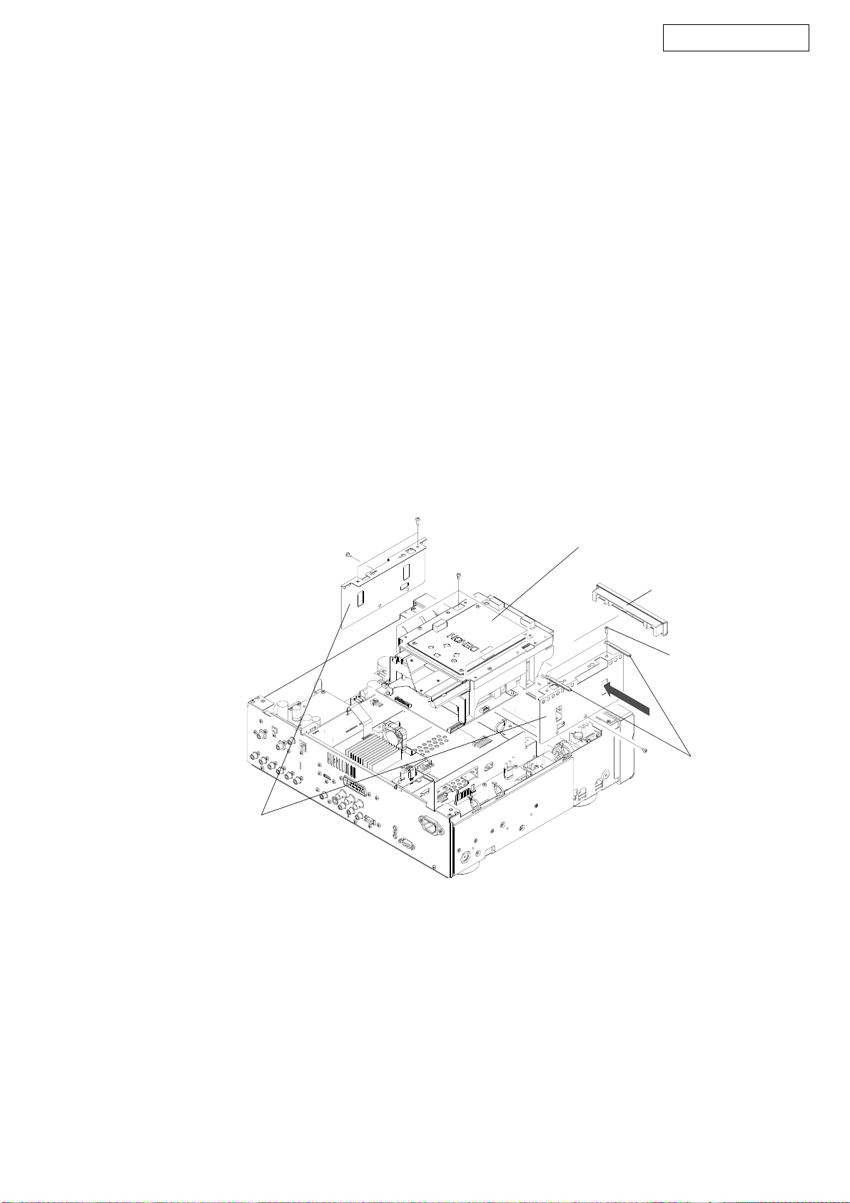
1. Topcover&Innercover
1.1. トップカバー
(1) 背面側から s ・ 1 のねじ 2 本と天・側面から s ・ 2 の
ねじ 9 本をはずします。
(2) 左右へ少し広げて m ・ 1:Topcover をはずします。
1.2. インナーカバー
(1) 天面から s ・ 3 のねじ 4 本をはずします。
(2) m ・ 2:Innercover をはずします。
1. Top cover & Inner cover
1.1. Top cover
(1) Remove 2 screws (s • 1) on the rear side and
9 screws (s • 2) on the top and the both sides.
(2) Widen the Top cover (m • 1) a little laterally, then detach
it with sliding.
1.2. Inner cover
(1) Remove 4 screws (s • 3) on the top side.
(2) Detach Inner cover (m • 2).
s • 2
s • 3
s • 1
m • 1: Top cover
m • 2: Inner cover
s • 2
s • 2
6
DVD-3930/3930CI
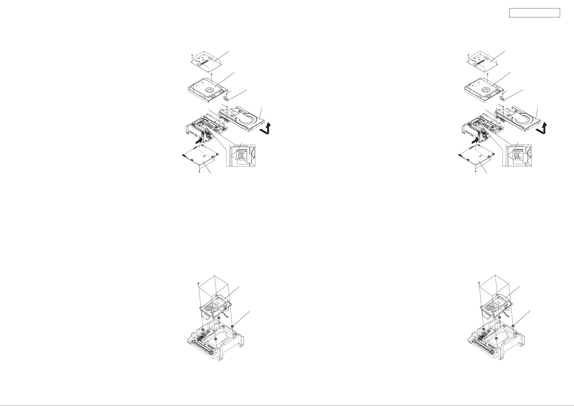
2. DVDmechanismass'y
2.1. ディスクトレイが電動でオープン出来る場合
(1) 電源を入れ「 OPEN/CLOSE 」ボタンを押して、ディスクト
レイを開きます。
(2) c ・ 1:Loaderpanelass'y を持ち上げてはずします。
(3) ディスクトレイを閉じます。
(4) 天面側から s ・ 4 のねじ 4 本と s ・ 5 のねじ 4 本をはずし
ます。
側面側から s ・ 1 のねじ 2 本をはずし、m ・ 3:Mecha
sidecover と c ・ 3:CordHolder2 個をはずます。
(5) メイン基板(GU-3749-1) よりワイヤー [CX131][CX211]
をはずします。
オーディオ ( デジタル ) 基板 (GU-3751-1) からワイヤー
[CY221][CY331]をはずします
(6) c ・ 2:DVDmechanismass'y をはずします。
2.2. ディスクトレイが電動でオープン出来ない場合
(1) 左側面の孔よりドライバー等を挿し込みメカユニット
のプレートギアを押してディスクトレイを開きます。
( 矢印方向 )
(2) 2-1.(2) 〜 (6) の作業に同じ。
2. DVD mechanism ass'y
2.1. When the Disc tray can be ejected electrically.
(1) Switch on, and press [OPEN/CLOSE] button to open the
Disc tray.
(2) Detach the Loader panel ass'y (c • 1) by lifting.
(3) Close the Disc tray.
(4) Remove 4 screws (s • 4) and 4 screws (s • 5) on the top
side.
Remove 2 side screws (s • 1), then detach the Mecha
side cover(m • 3).
(5) Disconnect [CX131] [CX211] from the MAIN P.W.B. (GU-
3749-1).
Disconect [CY221] [CY331] from the AUDIO (DIGITAL)
P.W.B. (GU-3751-1).
(6) Take the DVD mechanism ass'y (c • 2) off.
2.2. When the Disc tray cannot be ejected electrically.
(1) Insert a driver into the left hole, and push the Plate Gear
of the DVD Mechanism, to open the Disc Tray.
(Arrow direction)
(2) The same steps described on 2-1. (2)~(6).
s • 1
c • 3: Cord Holder
c • 2: DVD mechanism ass’y
c • 1: Loader panel ass’y
s • 4
s • 5
s • 4
m • 3: Mecha Side cover
s • 1
7
DVD-3930/3930CI
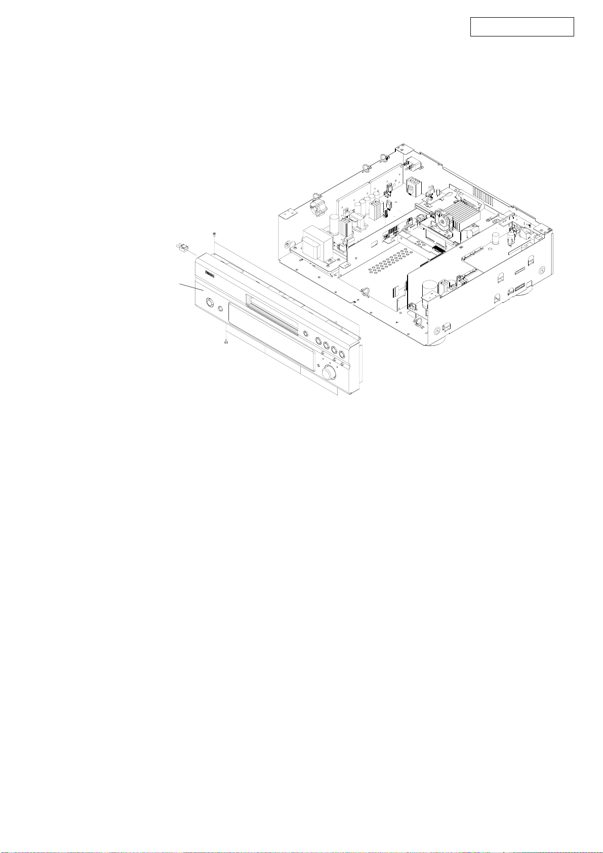
3. Frontpanelsubass'y
(1) a ・ 1:Frontpanelsubass'y からのワイヤー [CX031]
[CX025]をはずします。
(2) 天面から s ・ 3 のねじ 2 本と底面から s ・1のねじ 4 本を
はずし、a ・ 1:Frontpanelsubass'y をはずします。
3. Front panel sub ass'y
(1) Disconnect the wire [CX031] [CX025] connecting From
the Front panel sub ass'y (a • 1).
(2) Remove 2 top screws (s • 3) and 4 bottom screws (s • 1),
then detach the Front panel sub ass'y.
s •3
s •1
a • 1: Front panel sub ass’y
8
DVD-3930/3930CI
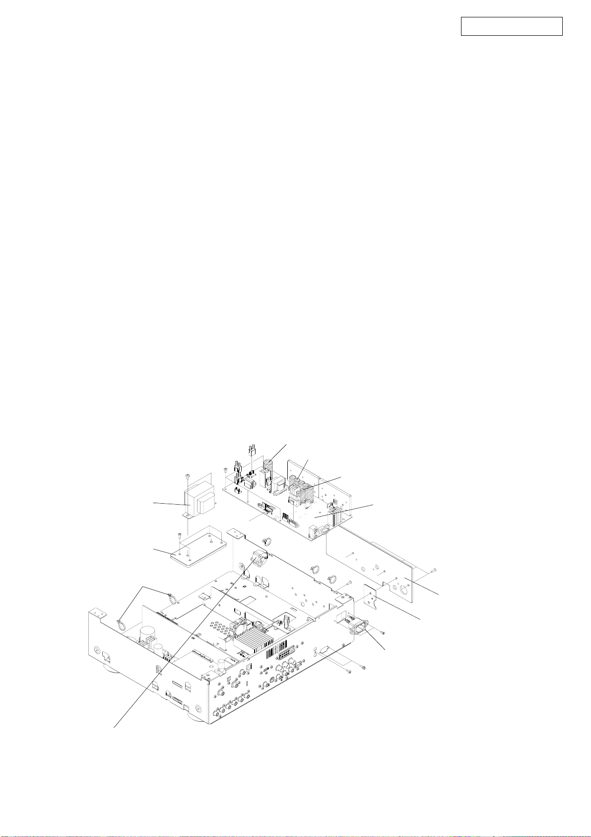
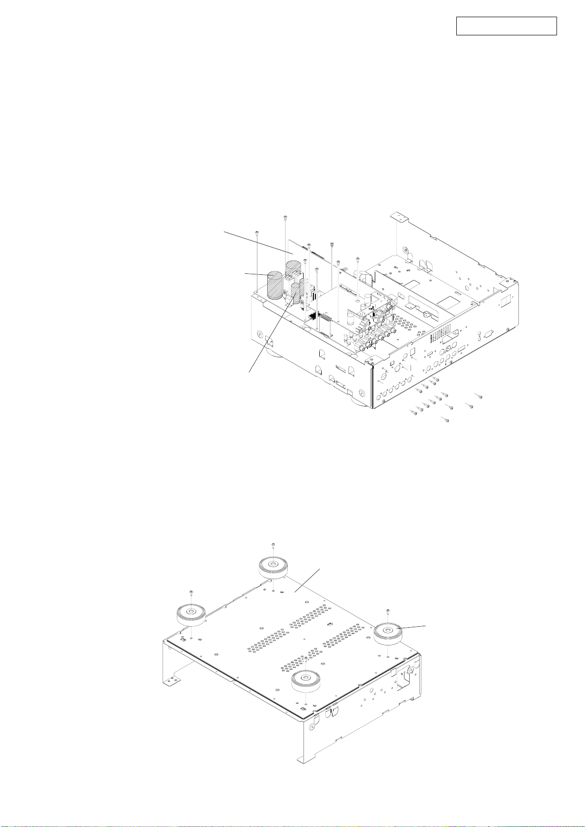
4. PowerP.W.B.ass'yetc.
4.1. 電源基板 ass'y
(1) 背面から s ・ 6 のねじ 1 本と s ・ 7 のナット 2 本をはずし
ます。
側面から s ・ 8 のねじ 5 本と天面から s ・ 4 のねじ 4 本
をはずします。
(2) m ・ 4:HeatPlate(Al) と m ・ 5:HeatPlate(Cu) をはず
します。
(3) c ・ 4:電源基板 ass'y からワイヤー [CX024][CX025]
[CX026][CX064][CW071]をはずします。
(4) c ・ 4:電源基板 ass'y をはずします。
電源基板 ass'y の廃棄時は、
C904、C913、C914、C916、C917、C919、C922、C955 電解
コンデンサを取外して WEEE 指令に基づく処理の事。
4.2. ACINLET
(1) 背面から s ・ 3 のねじ 2 本をはずします。
(2) c・5:ACINLETから STO コネクターをはずします。
(3) c・5:ACINLET をはずします。
4.3. フェライトコア& 3PVH ワイヤー
(1) シャーシ左側面のクランプバンド3箇所をカットします。
(2) c・6:フェライトコアと 3PVH ワイヤーをはずします。
4.4. 電源トランスとトランスベース
(1) 天面から s・10 のねじ 2 本をはずします。
(2) c・7:PowerTrans をはずします。
(3) 天面から s・9 のねじ 4 本をはずします。
(4) m・6:TransBase をはずします。
4. Power P.W.B. ass'y etc.
4.1. Power P.W.B. ass'y
(1) Remove 1 screw (s • 6) and 2 nut (s • 7) on the rear side.
Remove 5 side screws (s • 8) and 4 top screws(s • 3).
(2) Detach the Heat plate (Al) (m • 4) and Heat plate (Cu)
(m • 5).
(3) Disconnect the wire [CX024] [CX025] [CX026] [CW071]
[CX064] connecting Power P.W.B. ass'y (c • 4).
(4) Detach the Power P.W.B. ass'y (c • 4).
Thing to do abandonment based on WEEE directive de-
taching E-Capacitor of C904, C913, C914, C916, C917,
C919, C922, C955 when abandoning Power P.W.B.
ass'y(c • 4).
4.2. AC INLET
(1) Remove 2 rear screws (s • 3).
(2) Disconnect the STO terminals from AC inlet (c • 5).
(3) Detach the AC inlet (c • 5).
4.3. Ferrite core & 3P VH wire
(1) Cut 3 clamper on the left side of the chassis.
(2) Detach the Ferrite core & 3P VH wire (c • 6).
4.4. Power Trans & Trans Base
(1) Remove 2 top screw (s • 10).
(2) Detach the Power Trans (c • 7).
(3) Remove 4 top screw (s • 9).
(4) Detach the Trans Base (m • 6).
◆ C913, 914:Φ10 x h30.0mm: 1000uF/25V
◆ C916, 917, 919, 922, 955: Φ12.5 x h35.5mm: 5600uF/6.3V
c • 4: Power P.W.B. ass’y
s • 9
◆ C904: Φ16 x h40.0mm: 100uF/400V
c • 5: AC inlet
s • 3
s • 6
s • 7
c • 6: Ferrite core & 3P VH wire
p: Clamper
s • 8
s • 10
c • 7: Power trans
m • 6: Trans Base
m • 4: Heat Plate (Al)
m • 5: Heat Plate (Cu)
s • 4
9
DVD-3930/3930CI
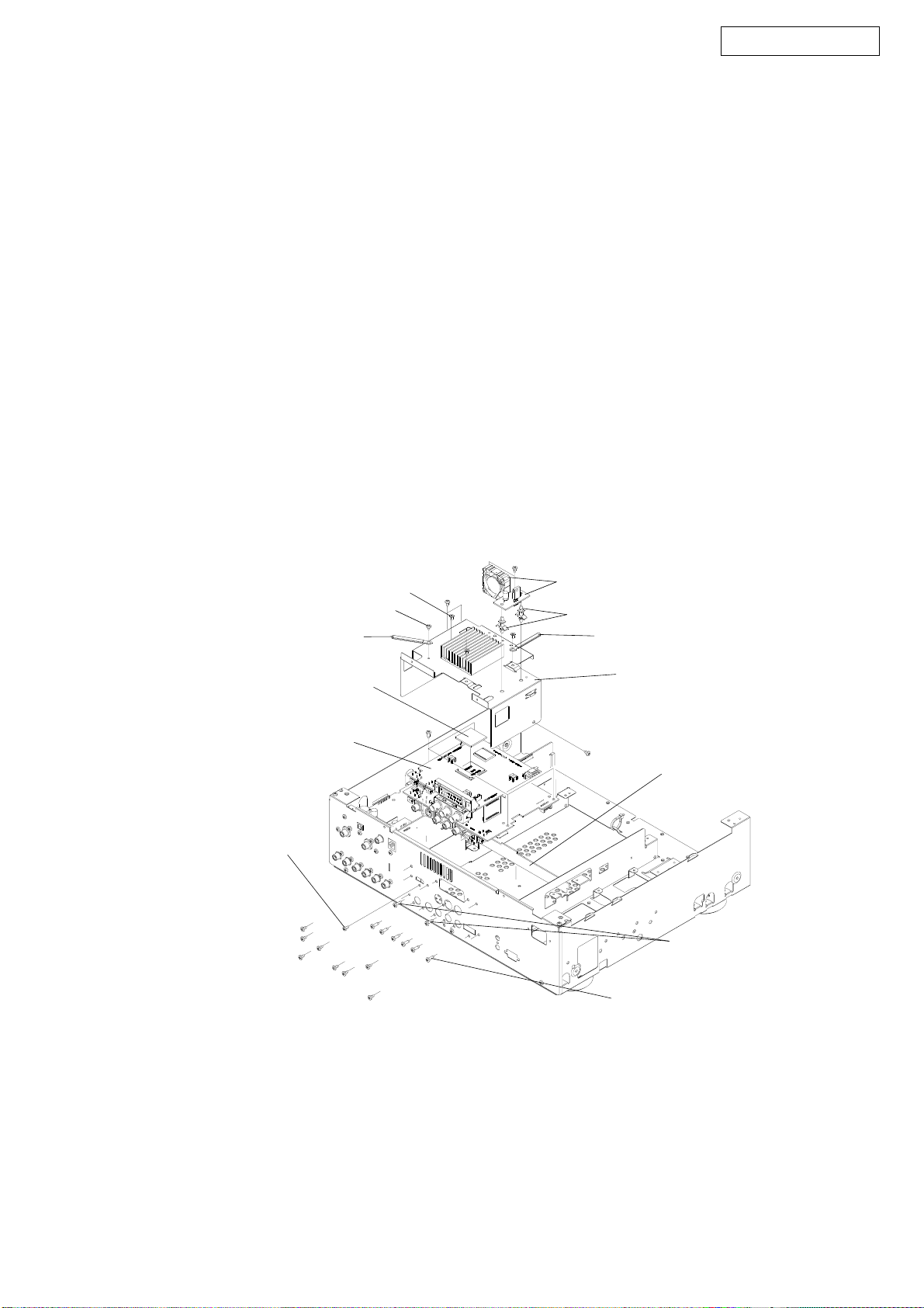
5. BlockofVideoP.W.B.
5.1. サポート板金 ass'y
(1) 背面の s ・ 1 のねじ 2 本、側面の s ・ 1 のねじ 1 本、天面
から s ・ 1 のねじ 2 本と s ・ 11 のねじ 3 本をはずします。
(2) デジタルビデオ基板 ass'y(GU-3752) よりワイヤー
[CY131][CY041(E2 のみ )] をはずします。
(3) 天面から s ・ 14 のねじをはずし、c ・ 3:コードホルダー
をはずします。(E2 モデル )
(4) 2 個の p ・ 1:PCB サポートと天面から s ・ 1 のねじ 2 本を
はずし、c ・ 8:FAN & FAN 電源基板をはずします。
(5) m ・ 7:サポート板金 ass'y をはずします。
(6) p ・ 2:ヒートシートをはずします。
5.2. Video 基板ブロック
(1) 背面側から s ・ 1 のねじ 6 本、s ・ 12 のねじ 5 本( 国内:
6、E2:7) と s ・ 13 のねじ 1 本と天面から s ・ 4 のねじ 4
本をはずします。
(2) c ・ 9 ビデオ基板ブロック (GU-3749-2/GU-3749-3/GU-
3750-6/GU-3750-7/GU-3750-8/GU-3752) をはずします。
(3) c ・ 10:M サポート基板をはずします。
5. Block of Video P.W.B.
5.1. Support bracket ass'y
(1) Remove 2 rear screws (s • 1) and a side screw (s • 1) and
2 top screws (s • 1) and 3 top screws (s • 11).
(2) Disconnect [CY131] [CY041 (only E2) ] from the D.Video
P.W.B. ass'y (GU-3752).
(3) Remove a top screw (s • 14), take the Cord Holder (p • 3)
off. ( only E2 )
(4) Remove 2 PCB Support (p • 1) and 2 top screws (s • 1),
take the FAN & FAN Power P.W.B. ass'y (c • 7) off.
(5) Take the Support bracket ass'y (m • 7) off.
(6) Take the Heat sheet (p • 2) off.
5.2. Block of Video P.W.B.
(1) Remove 6 screws (s • 1) and 5 (JP: 6, E2: 7) screws
(s • 12) and 1 screw (s • 13) on the rear side and 4 screws
(s • 4) on the top side.
(2) Take the Block of Video P.W.B. (GU-3749-2/GU-3749-3
/GU-3750-6/GU-3750-7/GU-3750-8/GU-3752) (c • 9) off.
(3) Detach the M.Support P.W.B. (c • 10) off.
m • 7: Support bracket ass’y
s • 1
s • 1
c • 10: M. Support P.W.B.
c • 9: Block of Video P.W.B. ass’y
s • 4
s • 11
s • 13
s • 12 (only
Japan
)
s • 1
s • 1
s • 12
s • 12 (only Europe)
p • 2: Heat sheet
c • 3: Cord Holder
(only Europe)
s • 14:
(only Europe)
c • 3: Cord Holder
p • 1: PCB Support
c • 8: FAN & FAN Power P.W.B.
10
DVD-3930/3930CI
6. BloackofAudioP.W.B.
6.1. オーディオ基板ブロック
(1) 背面から
s・1
のねじ 4 本と s ・ 12 のねじ 10 本と天面か
ら
s・4
のねじ 8 本をはずします。
(2)
c・11
:オーディオ基板ブロックからワイヤー[CY044] をは
ずします。
(3) c ・ 11:オーディオ基板ブロックをはずします。
c ・ 11:オーディオ基板ブロックの廃棄時は、
C814 、 C815 、 C854 、 C855 電解コンデンサを取外して
WEEE 指令に基づく処理の事。
7. Footass'y
(1) 底面の s ・ 4 のねじ 4 本をはずします。
(2) p ・ 3:Footass'y をはずします。
6. Block of Audio P.W.B.
6.1. Block of AUDIO P.W.B.
(1) Remove 4 screws (s • 1) and 10 screws (s • 12) on the
rear side and 8 screws (s • 4) on the top side.
(2) Disconnect the wire [CY044] connecting Block of AUDIO
P.W.B. (c • 11).
(3) Detach the Block of AUDIO P.W.B. (c • 11).
Thing to do abandonment based on WEEE directive de-
taching E-Capacitor of C814, C815, C854, C855 when
abandoning Block of AUDIO P.W.B. (c • 11).
7. Foot ass'y
(1) Remove 4 bottom screws (s • 4).
(2) Take the Foot ass'y (p • 3) off.
s • 4
c • 11: Block of Audio P.W.B.
s • 1
s • 12
◆ C854, 855:Φ30.0 x h50.0mm: 3300uF/50V
◆ C814, 815:Φ16.0 x h35.5mm: 470uF/50V
s • 4
m • 8: Chassis & Bottom cover & Rear panel
p • 3: Foot ass’y
11
DVD-3930/3930CI
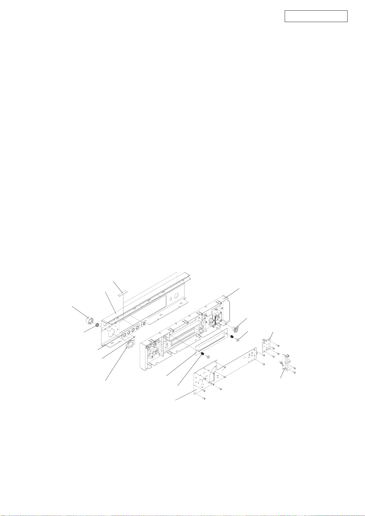
8. PartsonFrontpanelsubass'y(a ・ 1)
8.1. ディスプレイ基板
(1) s ・ 6 のねじ 10 本をはずします。
(2) c ・ 12:ディスプレイ基板をはずします。
(3) ワイヤー[CY052]をはずします。
(4) c ・ 13:S.ノブsubass'y と m ・ 9 バネをはずします。
8.2. 電源 SW-1 基板
(1) s ・ 6 のねじ 2 本をはずします。
(2) c ・ 14:電源 SW-1 基板をはずします。
8.3. 電源 SW-2 基板
(1) s ・ 6 のねじ 4 本をはずします。
(2) c ・ 15:P.SW-2 基板をはずします。
(3) c ・ 16:電源 2 次側ノブをはずします。
8.4. ブラインド ass'y
(1) s ・ 15 のねじ 2 本をはずします。
(2) m ・ 10:バネ 2 個と p ・ 3:ブラインド ass'y をはずしま
す。
8.5. インナーパネル
(1) 上下各 4 個のフックをはずします。
(2) p ・ 5:インナパネルをはずします。
8.6. フロントパネル
(1) p ・ 6:インナーパネルカット部品、3 個の p ・ 7:レンズ、
p ・ 8:ノブガイド、2 個の p ・ 9:ラバーをマイナスドラ
イバー等ではずします。
8. Parts on Front panel sub ass'y (a • 1)
8.1. Display P.W.B. ass'y
(1) Remove 10 screws (s • 6).
(2) Take the Display P.W.B. ass'y (c • 12) off.
(3) Disconnect [CY052].
(4) Take the Spring (m • 9) and the S. knob sub ass'y (c • 13)
off.
8.2. P. SW-1 P.W.B. ass'y
(1) Remove 2 screws (s • 6).
(2) Take the P. SW-1 P.W.B. ass'y (c • 14) off.
8.3. P. SW-2 P.W.B. ass'y
(1) Remove 4 screws (s • 6).
(2) Take the P. SW-2 P.W.B. ass'y (c • 15) off.
(3) Take the Power knob (SUB) ass'y (c • 16) off.
8.4. Blind ass'y
(1) Remove 2 screws (s • 14).
(2) Take the 2 Springs (m • 10) and the Blind ass'y (p • 3) off.
8.5. Inner panel
(1) Detach 4 top hooks and 4 rear hooks.
(2) Take the Inner panel (p • 5) off.
8.6. Front panel
(1) Detach the Part of Inner panel (p • 6), 3 Lens (p • 7), Knob
Guide (p • 8) and 2 rubber sheets (p • 9) by minus (-) driv-
er or etc.
p • 9: Rubber sheet
p • 8: Knob Guide
m • 10: Front panel
p • 6: Part of Inner panel
c • 12: Display P.W.B. ass’y
s • 6
s • 6
c • 15: P. SW-2 P.W.B. ass’y
c • 14: P. SW-1 P.W.B. ass’y
c • 16: Power knob (SUB) ass’y
p • 5: Inner panel
s • 15
c • 13: S. knob sub ass’y
m • 9: Spring
p • 7: Lens
p • 4: Blind ass’y
m • 9: Spring
s • 6
12
DVD-3930/3930CI
DIAGNOSTICS OF OPTICAL PICKUP
AND REPLACING TRAVERSE UNIT
Make failure diagnostics of the Optical Pickup as follows.
If the laser drive current (Iop) becomes more than 1.5 times of
the initial value, the Optical Pickup should be replaced.
The laser drive current initial value is checked by "Iop checked
Method" of next page.
In case of replacing the Pickup, change the whole part of the
Traverse Unit.
No mechanical adjustment is necessary after the replace-
ment.
光ピックアップの故障診断とトラバース
ユニットの交換
次の順序で故障診断を行ってください。
レーザー駆動電流 Iop 値が初期値の 1.5 倍以上になっている
場合は光ピックアップ交換の目安となります。
レーザー駆動電流初期値は、次ページ "Iop 値の確認方法 " で
確認できます。
ピックアップ交換の場合は、トラバースユニット単位での交
換となります。メカの調整は不要です。
レーザー駆動電流初期値 :
Laser drive current initial value:
FLDisplay(Thedisplaypartof13digits)
12345678910111213
T22―mmmm―nnnn
FLDisplay(Thedisplaypartof13digits)
12345678910111213
T2 1 ―mmmm―nnnn
Disc no read, unsteady playback, etc.
Laser drive current (Iop) check
HF wave form check
(Refer to WAVE FORMS)
Traverse Unit replacing
Laser current (Iop) memorizing after replacement
Present value exceeds the ini-
tial value by 1.5 times
ディスクを読み込まない
スムーズに再生しない、等
レーザー駆動電流 Iop 値の確認
HF 波形の確認
(WAVEFORMS参照)
トラバースユニット交換
交換後にレーザー電流値の記憶
現在値が初期値の
1.5 倍になっている
CD:
DVD:
13
DVD-3930/3930CI
1. Iop checked Method
Select the laser ON/OFF (CD/DVD) mode of the test mode,
and check the lop value of DVD laser or CD laser.
(See page 19 for test mode.)
1.1. DVD laser current check
(1) Press the SKIP REV or SKIP FWD button to display the
laser current value, and then select T22.
(2) Check the current value of Iop (nnnn).
( − : Off, DVD laser, Initial value: mm.mm [mA],
Current value: nn.nn [mA])
1.2. CD Laser current check
(1) Press the SKIP REV or SKIP FWD button to display the
laser current value, and then select T21.
(2) Check the current value of Iop (nnnn).
( − : Off, CD laser, Initial value: mm.mm [mA],
Current value: nn.nn [mA])
2. Note for Handling the Laser Pick-Up
The protection for the damage of laser diode.
If you want to change the optical device unit from any other
units, you must keep the following.
(1) It should be done at the desk already took measures the
static electricity in care of removing the OPU's (Optical
device unit) connector cable.
(2) Workers should be put on the "Earth Band".
(3) It should be done to add the solder to the short land to
prevent the broken Laser diode before removing the 24P
FFC cable.
(4) Don't touch OPU's connector parts carelessly.
3. Replacement of the Laser Pick-up
(Traverse Unit)
Check the Iop (Laser drive current)
If the present Iop (current) value exceeds.+150% of the ini-
tial value, replace the Traverse unit (Laser Pick-up) with a
new one.
FLDisplay(Thedisplaypartof13digits)
12345678910111213
T2 L a s e r O n O f f
FLDisplay(Thedisplaypartof13digits)
12345678910111213
T22―mmmm―nnnn
FLDisplay(Thedisplaypartof13digits)
12345678910111213
T2 1 ―mmmm―nnnn
1. Iop 値の確認方法
レーザー駆動電流を確認する場合は、テストモードのレー
ザー ON/OFF(CD/DVD) モードを選択して、DVD レーザー
または CD レーザーの lop 値を確認します。
(詳細は 19 ページ、テストモード参照)
1.1. DVD レーザー電流確認
(1) レーザー電流値を表示する場合は、SKIPREV,SKIPFWD
ボタンを押し、T22 を選択します。
(2) 現在の lop 値 (nnnn) を確認します。
( −:消灯、DVD レーザー、初期値:mm.mm[mA],
現在値:nn.nn[mA])
1.2. CD レーザー電流確認
(1) レーザー電流値を表示する場合は、SKIPREV,SKIPFWD
ボタンを押し、T21 を選択します。
(2) 現在の lop 値 (nnnn) を確認します。
( −:消灯、CD レーザー、初期値:mm.mm[mA],
現在値:nn.nn[mA])
2. レーザーピックアップの取扱注意
レーザーダイオードの破壊防止。
光素子ユニットを交換するときは、以下を遵守してくださ
い。
(1) 光素子ユニットの接続ケーブルをはずすときは、静電対
策を行ったデスク上で作業してください。
(2) 作業者は、リストストラップを使用してください。
(3) レーザーダイオードの破壊防止のため、24PFFC ケーブ
ルをはずす前にランドを半田付けショートしてくださ
い。
(4) 光素子ユニットのコネクタ部に触れないでください。
3. レーザーピックアップ ( トラバースユニッ
ト ) の交換
Iop( レーザー駆動電流)をチェックします。
現在の Iop値が初期値の 150%を越えている場合、トラバー
スユニット(レーザーピックアップ)を交換してください。
FL 管の表示 (13 桁の表示部 )
12345678910111213
T2 L a s e r O n O f f
FL 管の表示 (13 桁の表示部 )
12345678910111213
T22―mmmm―nnnn
FL 管の表示 (13 桁の表示部 )
12345678910111213
T2 1 ―mmmm―nnnn
14
DVD-3930/3930CI
4. Rewriting the default value of the laser
current
To rewrite the default value of the laser current, press the
PLAY button for at least 5 seconds while the CD or DVD la-
ser current is displayed, then press the SKIP FWD or SKIP
REV button to select T23. (For details, see "Iop checked
Method" on page 13.)
If the PLAY button is pressed while T23 is displayed, the
current value is displayed at "mmmm" and stored in the EE-
PROM.
5. Resetting the accumulated laser on time
To clear the accumulated laser on time, press the PLAY but-
ton while the accumulated laser on time is displayed (TB1,
TB2 : For details, see "Test Mode" on page 19.) until "*" ap-
pears at the fourth position, then press the SKIP FWD or
SKIP REV button to select TB3.
If the PLAY button is pressed while TB3 is displayed, the
accumulated laser on time of CD and DVD is cleared.
When TB1 or TB2 is selected with the SKIP FWD or SKIP
REV button, "nnnnnnn" is displayed as 0 so you can check.
( − : Off, Y:1: CD, 2: DVD, nnnnnnn: Hour [h])
FLDisplay(Thedisplaypartof13digits)
12345678910111213
T2 3 ―mmmm―――――
FLDisplay(Thedisplaypartof13digits)
12345678910111213
TBY―――nnnnnnn
4. レーザー電流初期値の書き換え方法
レーザー電流の初期値を書き換えるには、CD または DVD
レーザー電流が表示されている時に PLAY ボタンを 5 秒以
上押し、次に SKIPFWD ボタンまたは SKIPREV ボタンを押
して T23 を選択します。(詳細は 13 ページ、Iop 値の確認
方法参照)
T23 表示時に PLAY ボタンを押と、mmmm 部に現在値を表
示し、EEPROM に保存します。
5. レーザー ON 累積時間のリセット方法
レーザーON 累積時間をクリアするには、レーザーON 累
積時間表示 (TB1,TB2) の時(詳細は 19 ページ、テストモー
ド参照)にPLAY ボタンを 4 桁目に ' * ' が表示されるまで
押し、SKIPREV ボタンまたはSKIPFWD ボタンを押し TB3
を表示させます。
TB3 表示時にPLAY ボタンを押すと、CD 及び DVD レーザー
ON 累積時間をクリアします。
SKIPREV ボタンSKIPFWD ボタンで TB1 または TB2 を選択
すると、nnnnnnn 部が 0 表示となり確認できます。
( −:消灯、Y:1:CD,2:DVD、nnnnnnn:時間 [h])
FL 管の表示 (13 桁の表示部 )
12345678910111213
T2 3 ―mmm m―――――
FL 管の表示 (13 桁の表示部 )
12345678910111213
TBY―――nnnnnnn
15
DVD-3930/3930CI
How to Replace Traverse Unit
1. Preparing for Replacement
(1) Removing Clamp Base Damper
Remove 4 pcs of 2.6mm machine screw (a), and detach the
Clamp Base Damper upward.
(2) Removing Clamp Base
Remove 2 pcs of 3mm P-tight screw (b), and detach the Clamp
Base upward.
(3) Ejecting Loader
Through the left rectangular hole of the Mechanism Unit, push
the slider with a ruler or driver unit the Traverse portion lowers
and the Loader comes out a little.
(4) Removing Loader
• Remove 2 pcs of 3mm P-tight screw (c) on the Loader Holder
left.
• Remove 2 pcs of 3mm P-tight screw (d) on the Loader Holder
right, then pull up the Bearing Plate.
• Fully pull out the Loader forward, and lift up to take it out.
(5) Shorting Pickup
To protect the Pickup from static electricity, short-circuit 1 posi-
tions as shown in figure.
(6) Removing Main P.W.B. Ass’y
Remove 3 pcs of 3mm P-tight screw (e), and detach the Main
P.W.B. Ass’y downward.
2. Replacing Traverse Unit
(1) Removing Wires
• CX241: 24P-FFC for Pickup
• CX151: 15P-FFC for Spindle
• CX051: 5P-PH wire for PU Side
(2) Removing Traverse Unit
Remove 4 pcs of special screw (f) and dampers, then take out
the Traverse Unit upward.
(3) Mounting Traverse Unit
Mount the Traverse Unit following the reverse order.
(a)
(b)
(b)
(c)
(d)
(4)
(3)
(e)
Clamp Base Damper
Clamp Base
Bearing Plate
Loader
Holder
Main P.W.B. Ass’y
Solder to short-circuit
Short-circuit with solder
(f)
Traverse Unit
Damper
トラバースユニットの交換方法
1. トラバースユニット交換準備
(1) クランプベースダンパーのはずしかた
2.6mm マシンネジ (a)4 本をずして、クランプベースダンパー
を上へはずします。
(2) クランプベースのはずしかた
3mmP タイトネジ (b)2 本をはずして、クランプベースを上へ
はずします。
(3) ローダーを開く
メカユニットの左側角孔より、スライダーを定規やドライバー
でトラバース部が下がってローダーが少し開くまで押します。
(4) ローダーのはずしかた
・ローダー左のホルダー部より 3mmP タイトネジ (c)2 本をは
ずします。
・ローダー右側より 3mmP タイトネジ (d)2 本をはずし、ベア
リングプレートを上へはずします。
・ローダーを前面へ引き出し、止まった所で上へはずします。
(5) ピックアップのショート
トラバースユニットのピックアップの静電保護のため、1 箇所
ショートします。
(ショート箇所は、右図参照)
(6) メイン基板 ASS'Y のはずしかた
3mmP タイトネジ (e)3 本をはずし、基板を下へはずします。
2. トラバースユニットの交換
(1) トラバースユニットのワイヤーをはずす
・CX241:ピック用 24P-FFC
・CX151:スピンドル用 15P-FFC
・CX051:PU スライド用 5P-PH ワイヤー
(2) トラバースユニットをはずす
特殊ネジ (f)4 本とダンパー 4 個をはずし、トラバースユニット
を上にはずします。
(3) トラバースユニットの取り付け
逆の手順で、トラバースユニットを取り付けます。
(a)
(b)
(b)
(c)
(d)
(4)
(3)
(e)
クランプベースダンパー
クランプベース
ベアリングプレート
ローダー
ホルダー
メイン基板 Ass'y
半田ショート部
半田ショート拡大図
(f)
トラバースユニット
ダンパー
16
DVD-3930/3930CI
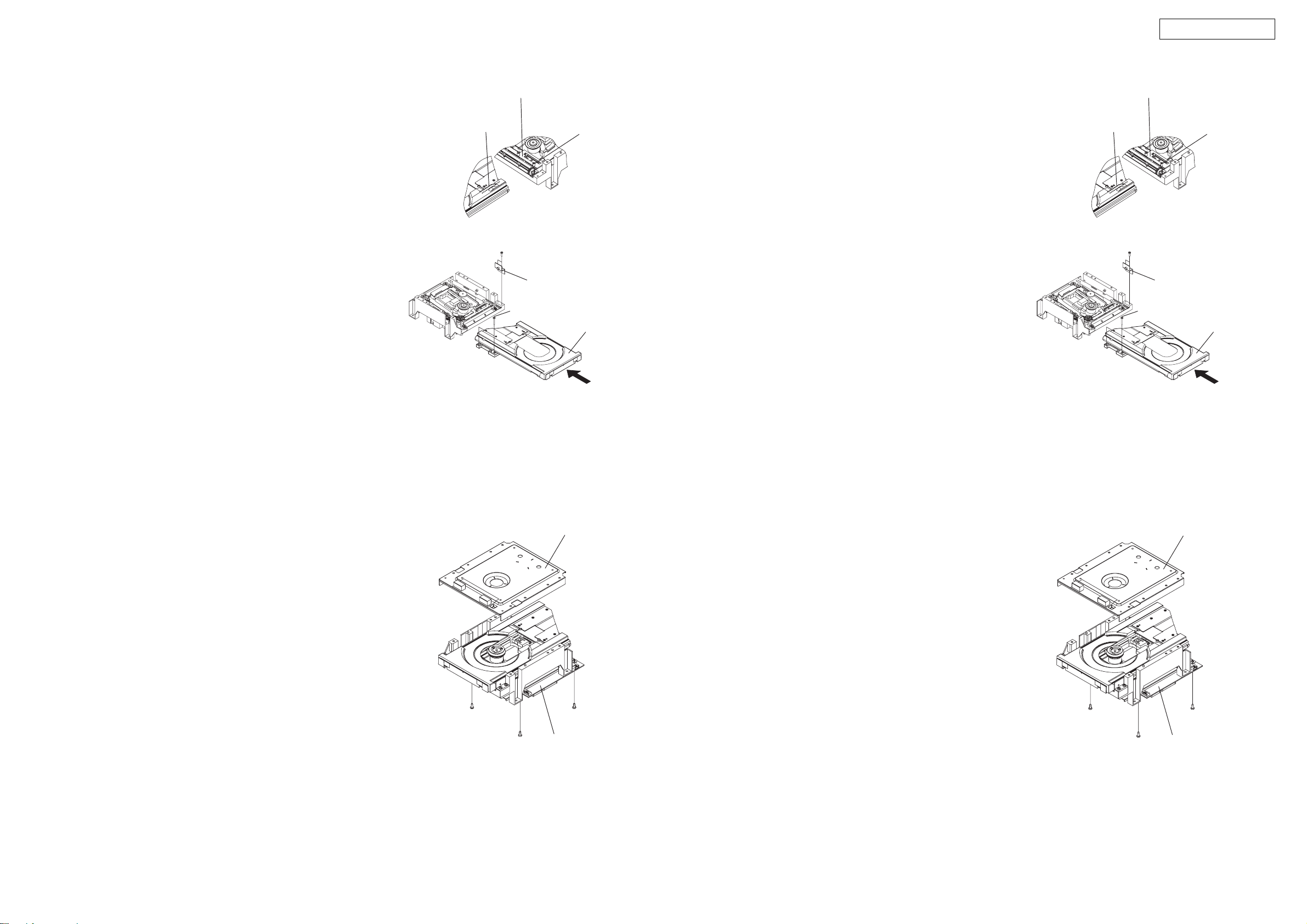
3. Installing Loader
(1) Inserting Loader
Set and push the Loader to the arrow direction until it stops.
When installing the Loader, move Plate Gear to right before-
hand so as that the boss of the Plate Gear fits in the backside
groove of the Loader. (See figure right)
(2) Fixing Loader
Fix the Loader with each 2 screws (c) and (d).
4. Assembly (1)
(1) Assembling Main P.W.B. Ass’y
Fix the Main P.W.B. Ass’y with 3 pcs of 3mm P-tight screw (e).
(2) Removing Pickup-short Solder
After connecting 24P-FFC of the Pickup with P.W.B., remove
solder from 1 shorted positions.
(3) Temporary Positioning Clamp Base
To protect your eyes from laser light, put the Clamp Base tem-
porarily.
(4) Positioning up Traverse Unit
Connect the following wires of the Mechanism Unit, and operate
it.
• CY132: 13P-PH wire for power
• CX212: 21P-FFC wire from Display P.W.B.
Turn on the power to the unit, and press “OPEN/CLOSE” button
to close the Loader.
The Traverse Unit rises up. (display: 0h00m00s)
Pull out Loader forward, and life up to take it out.
(d)
(c)
Plate Gear
Groove
Boss
Bearing Plate
Loader
(e)
(e)
(e)
Clamp Base
Main P.W.B. Ass’y
3. ローダーの組み立て
(1) ローダーの挿入
ローダーを矢印の方向へ止まるまで押しこみます。
ローダーを組み込み時、プレートギアのボスがトレイ裏面の
溝に合うようにプレートギアを右側へ寄せておきます。
(右図参照)
(2) ローダーの取り付け
(c)、(d) のネジ各 2 本を取り付けます。
4. 組み立て(1)
(1) メイン基板 ASS'Y の取り付け
3mmP タイトネジ (e)3 本で基板を取り付けます。
(2) ピックアップのショートをはずす
ピックアップの 24PFFC を基板へ接続後、1 箇所のショートを
はずします。
(3) クランプベースの仮置き
レーザーから目を保護するため、クランプベースを仮置きし
ます。
(4) トラバースユニットをアップする
メカユニットの下記ワイヤーを接続し、メカを動作させます。
・CY132:電源用の 13P-PH ワイヤー接続
・CX212:ディスプレイ基板からの 21P-FFC ワイヤー接続
セットの電源を入れ、ローダー開閉ボタンで、CLOSE させます。
トラバースユニットがアップします。
(0h00m00s:表示)
ローダーを前後に引き出し、止まったところで上へはずしま
す。
(d)
(c)
プレートギア
溝部
ボス
ベアリングプレート
ローダー
(e)
(e)
(e)
クランプベース
メイン基板 Ass'y
17
DVD-3930/3930CI
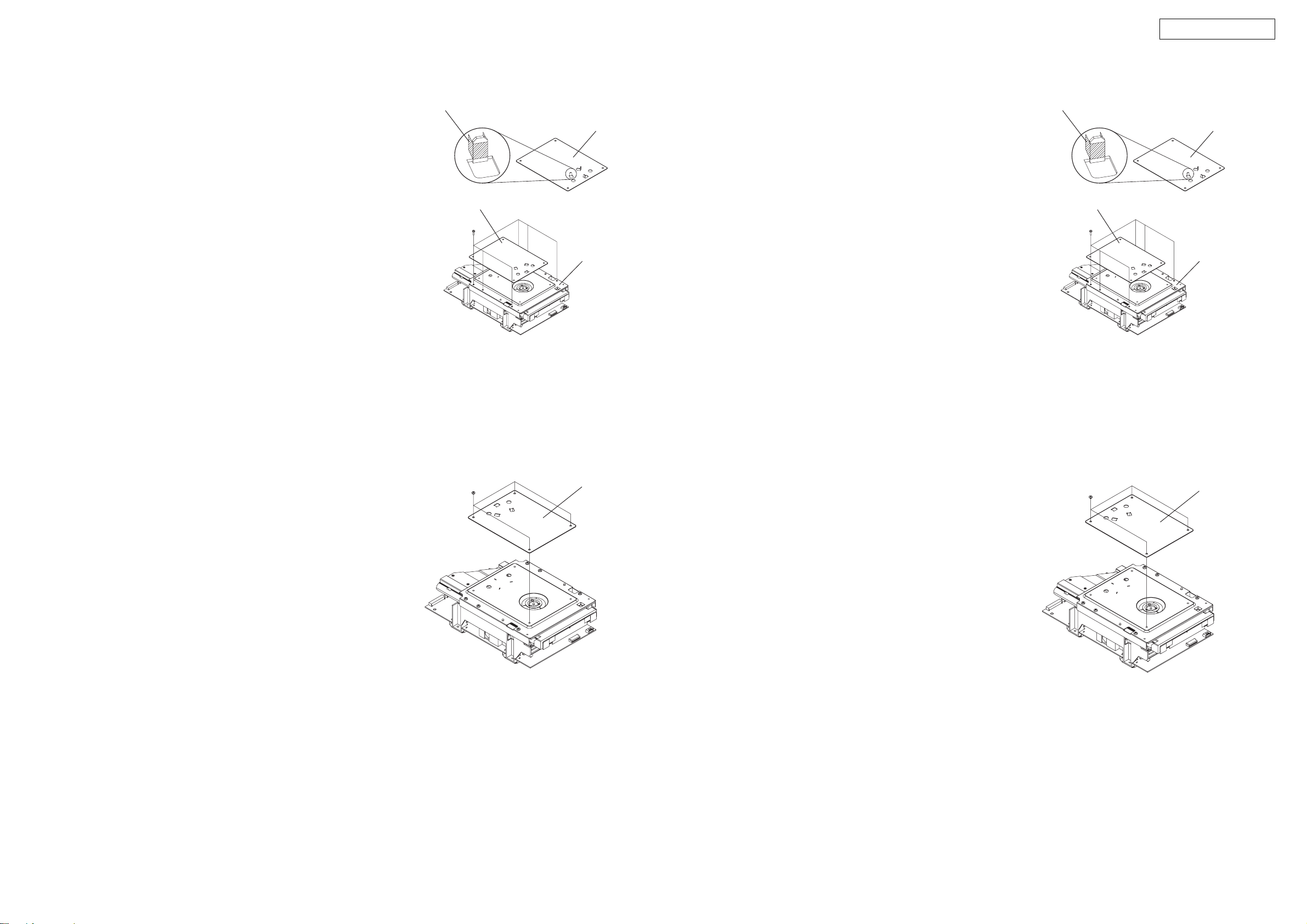
5. Assembly (2)
(1) Attaching Tape to Clamp Base Damper
Attach acetate cloth tape to 3 projections of the Clamp Base
Damper backside.
(2) Assembling Clamp Base
Set the Clamp Base Damper with positioning for clamper by 3
projections.
Fix the Clamp Base with 6 pcs of 3mm -tight screw (b).
6. Assembly (3)
(1) Detaching Tape from Clamp Base Damper
Detach acetate cloth tape from 3 projections of the Clamp Base
Damper backside.
(2) Assembling Clamp Base Damper
Set the Clamp Base Damper to the Clamp Base contrary to the
direction set in step above.
Fix the Clamp Base Damper with 4 pcs of 3mm S-tight screw
(a).
(b)
Acetate Cloth Tape
Clamp Base Damper
Clamp Base Damper
Clamp Base
(a)
Clamp Base Damper
5. 組み立て(2)
(1) クランプベースダンパーへのアセクロ貼り付け
クランプベースダンパー裏面の突起 3 箇所へアセテートクロ
ステープを貼り付けます。
(2) クランプベースの取り付け
クランプベースダンパーを挿入し、3 箇所の突起でクランパー
の位置決めをおこないます。3mmP タイトネジ (b)6 本で、ク
ランプベースを取り付けます。
6. 組み立て(3)
(1) クランプベースダンパーからアセクロをはがす
クランプベースダンパー裏面の突起 3 箇所からアセテートク
ロステープをはがします。
(2) クランプダンパーベースの取り付け
クランプベースダンパーを、クランプベースに先程と反対向
きに挿入します。3mmS タイトネジ (a)4 本で、クランプベー
スダンパーを取り付けます。
(b)
アセテートクロステープ
クランプベースダンパー
クランプベースダンパー
クランプベース
(a)
クランプベースダンパー
18
DVD-3930/3930CI
SERVICE MODE
1. Aging Mode
(1) preparation
(a) Equipment used: Any one of DVD Karaoke Disc (containing more than 10 titles).
(b) Unit setting : No spec other than the following procedure (Aging mode).
At the tray open status, press the “POWER” button to turn on the power while pressing the “PLAY” and “OPEN/CLOSE” buttons
for DVD operation simultaneously. mark on the FL lights, and the unit is set to the heat run mode.
(2) procedure
(a) According the above, set to the aging mode.
(b) Set a DVD Karaoke disc to the tray and press the “PLAY” button once. mark on the FL blinks, and aging operation (after
playback title-1 and title-10 of the disc, the tray open/close is made automatically, then playback the title-1 again) starts.
This aging operation continues automatically until it is stopped or it stops caused by an error. In case of some error in DVD, the
following error messages are displayed on the FL.
2. Initial Setting Mode
(1) Preparation
(a) Equipment used: None
(b) Unit setting: No spec other than the following procedure.
(2) Procedure
(a) Initialize the DVD player when µcom, peripheral parts of µcom, or Main P.W.B. has been replaced in servicing.
(b) Carry out the following to restore factory setting mode.
At the player stop condition, press 2 buttons for DVD operation (“PLAY” and “ SKIP FWD”) until “INITIALIZE” appears
and disappears in the FL.
(“Initialized” appears and disappears on the TV screen.)
(c) All user setting will be lost and its factory setting will be restored when this initialization is made. Be sure to memorize your setting
for restoring again after the initialization.
3. µcom Firm Check Mode
(1) Preparation
(a) Equipment used: None
(b) Unit setting: No spec other than the following procedure.
(2) Procedure
(a) Press the “POWER” button to turn on the power while pressing the “PLAY” and “OPEN/CLOSE” buttons for DVD operation si-
multaneously.
(b) DVD µcom and other µcom firm check mode.
This mode is for displaying the status of each µcom employed.
・Push remote contraller “3265”.
・DVD µcom firm: Press the “MENU” button.
・Each time the “MENU” button on the remote control unit is pressed, µcom firm is displayed one after another.
Ex.: [BE 8284, MAKE DAY 522, DSP 8250, IP 060621]
No. Error contents FL display
1 Tray Error ERROR 01
2 Bad Disc ERROR 02
3 Search Error ERROR 03
4 Read Error ERROR 04
サービスモードについて
1. エージングモード
(1) 準備
(a) 使用機器:DVD カラオケディスク(10 タイトル以上の物)。
(b) 本体設定:下記設定以外規定無。
(エージングモード)
トレイを開けた状態で DVD ユニットの「PLAY ボタン」+「OPEN/CLOSE ボタン」を同時押ししながら「電源ボタン」を押
してセットの電源を入れると、FL 管の マークが点灯し、ヒートランモードに設定される。
(2) 手順
(a) 上記手順でエージングモードに設定する。
(b) トレイに DVD カラオケディスクを入れ、「PLAY ボタン」を 1 回押して、FL 管の マークが点滅になると、「ディスクの
タイトル 1 とタイトル 10 を再生した後、トレイを自動で開 / 閉し、再度タイトル 1 の再生を行う。」エージング動作になり
ます。停止させるか、エラーにて停止するまでこの動作を自動で繰り返します。DVD 部にエラーが発生した場合は、FL 管に
下表のエラーが表示されます。
2. 初期設定モード
(1) 準備
(a) 使用機器:無
(b) 本体設定:下記手順以外規定無。
(2) 手順
(a) サービスにて、マイコンやマイコン周辺部分やメイン基板を交換した場合は、DVD プレーヤーの初期化を行ってくださ
い。
(b) セットの初期化を下記の手順で行い、工場出荷モードに設定する。
セットが停止状態にて、DVD 操作部の「PLAY ボタン」+「 (SKIPFWD) ボタン」の同時押しを FL 管に
"INITIALIZE" が表示され消えるまで押します。(TV 画面には初期化しましたが表示され消えます。)
(c) 初期化を行うとお客様が設定した内容が工場出荷状態に戻りますので、あらかじめ設定内容を控えておき初期化後に再設定
してください。
3. マイコンファームチェックモード
(1) 準備
(a) 使用機器:無
(b) 本体設定:下記手順以外規定無。
(2) 手順
(a) DVD 操作部の「PLAY ボタン」と「OPEN/CLOSE ボタン」を同時押ししながらセットの「電源ボタン」を押し電源を入れ
ます。
(b) DVD マイコン及びその他マイコンのファーム確認モード。
搭載されている各マイコンのファーム状態を表示します。
・数字キーで「3265」と入力します。
・DVD マイコンのファーム:リモコンの「メニューボタン」を押します。
・リモコンのメニューボタンを押すたびにマイコンファームを次々と表示します。
表示例:〔BE8284 、 MAKEDAY522 、 DSP8250 、 IP060621〕
No. エラー内容 FL 管表示
1 トレイエラー ERROR01
2 不良ディスク ERROR02
3 サーチエラー ERROR03
4 リードエラー ERROR04
19
DVD-3930/3930CI
4. Test mode
(1) Entering the test mode
To enter the test mode, press the STOP and SKIP FWD buttons simultaneously while in the heat run mode.
Basically, enter the test mode while in the stop mode after the disc is loaded.
(The heat run mode is entered by pressing the OPEN/CLOSE and PLAY buttons simultaneously to turn on the AC power.
When the heat run mode is set, the PLAY and PAUSE indicators light.)
Press OPEN/CLOSE + PLAY buttons simultaneously
Power turns on
Press STOP + SKIP FWD buttons simultaneously PLAY button
Test mode Aging mode
FL tube display when test mode entered
(2) Selecting the mode
The following modes are available.
(1) FL tube lighting mode : T0
(2) Tray open/close mode : T1
(3) Laser on/off (CD/DVD) mode : T2
(4) Servo adjustment value display mode : T3
(5) Servo properties measurement mode : TA
(6) Trace mode (error rate display) : T7
(7) Accumulated laser on time : TB
(8) Color bar output mode : TC
(9) Monitor terminal setting mode : TD
(10) SACD watermark signal quality checking mode : TE
(11) Digital video circuitry flash ROM writing mode : TF
① When the SKIP FWD button is pressed after entering the test mode, the display switches in the order: T0, T1, T2, T3, T7, TA,
TB, TC, TD, TE, TF, T0 …
FLDisplay(Thedisplaypartof13digits)
12345678910111213
TEST MODE
FLDisplay(Thedisplaypartof13digits)
12345678910111213
T0 F L D i s p l a y
FLDisplay(Thedisplaypartof13digits)
12345678910111213
T1 O p e n / C l o s e
FLDisplay(Thedisplaypartof13digits)
12345678910111213
T2 L a s e r O n O f f
FLDisplay(Thedisplaypartof13digits)
12345678910111213
T3 S e r v o A d j
FLDisplay(Thedisplaypartof13digits)
12345678910111213
T7 T r a c e M o d e
FLDisplay(Thedisplaypartof13digits)
12345678910111213
TA F o c us T r a c k
4. テストモード
(1) テストモードの設定
テストモードの設定はヒートランモード時に STOP ボタンと SKIPFWD ボタンを同時押しで行う。
基本的にディスクローディング後の停止状態でテストモードに設定する。
( ヒートランモードの設定は OPEN/CLOSE ボタンと PLAY ボタンを同時押ししながらセットの電源を入れる。
ヒートランモードになると PLAY インジケータと PAUSE インジケータが点灯する。)
OPEN/CLOSE + PLAY ボタンの同時押し
電源ON
STOP + SKIPFWD ボタンの同時押し PLAY ボタン
テストモード エージングモード
テストモード設定時の FL 管表示
(2) モードの選択
モードには、次のモードがある。
(1)FL 管点灯モード : T0
(2) トレイ OPEN/CLOSE モード : T1
(3) レーザー ON/OFF(CD/DVD) モード : T2
(4) サーボ調整値表示モード : T3
(5) サーボ特性測定モード : TA
(6) トレースモード ( エラーレート表示 ) : T7
(7) レーザー ON 累積時間 : TB
(8) カラーバー出力モード : TC
(9) モニタ端子設定モード : TD
(10)SACD ウォーターマーク信号品質確認モード : TE
(11)DIGITALVIDEO 回路フラッシュ ROM 書込みモード : TF
①テストモード中に SKIPFWD ボタンを押すと、T0,T1,T2,T3,T7,TA,TB,TC,TD,TE,TF,T0…の順に表示される。
FL 管の表示 (13 桁の表示部 )
12345678910111213
TEST MODE
FL 管の表示 (13 桁の表示部 )
12345678910111213
T0 F L D i s p l a y
FL 管の表示 (13 桁の表示部 )
12345678910111213
T1 O p e n / C l o s e
FL 管の表示 (13 桁の表示部 )
12345678910111213
T2 L a s e r O n O f f
FL 管の表示 (13 桁の表示部 )
12345678910111213
T3 S e r v o A d j
FL 管の表示 (13 桁の表示部 )
12345678910111213
T7 T r a c e M o d e
FL 管の表示 (13 桁の表示部 )
12345678910111213
TA F o c us T r a c k
20
DVD-3930/3930CI
② When the SKIP REV button is pressed, the display switches in the opposite order from ① above, starting from the current position
(for example, if currently at TA, it switches as follows: T7, T3, T2, T1, T0, TF, TE, TD, TC, TB …).
¦
¦
¦
FLDisplay(Thedisplaypartof13digits)
12345678910111213
TB L a s e r O n T i m
FLDisplay(Thedisplaypartof13digits)
12345678910111213
TC C o l o r B a r
FLDisplay(Thedisplaypartof13digits)
12345678910111213
TD M o n i t o r
FLDisplay(Thedisplaypartof13digits)
12345678910111213
TE S A C D
FLDisplay(Thedisplaypartof13digits)
12345678910111213
TF R S 2 3 2C S E L
FLDisplay(Thedisplaypartof13digits)
12345678910111213
T7 T r a c e M o d e
FLDisplay(Thedisplaypartof13digits)
12345678910111213
T3 S e r v o A d j
FLDisplay(Thedisplaypartof13digits)
12345678910111213
T2 L a s e r O n O f f
② SKIPREV ボタンを押すと現在表示されている点から①の逆順 ( 現在表示されている点が TA であれば、
T7,T3,T2,T1,T0,TF,TE,TD,TC,TB…の順 ) に表示される。
¦
¦
¦
FL 管の表示 (13 桁の表示部 )
12345678910111213
TB L a s e r O n T i m
FL 管の表示 (13 桁の表示部 )
12345678910111213
TC C o l o r B a r
FL 管の表示 (13 桁の表示部 )
12345678910111213
TD M o n i t o r
FL 管の表示 (13 桁の表示部 )
12345678910111213
TE S A C D
FL 管の表示 (13 桁の表示部 )
12345678910111213
TF R S 2 3 2 C S E L
FL 管の表示 (13 桁の表示部 )
12345678910111213
T7 T r a c e M o d e
FL 管の表示 (13 桁の表示部 )
12345678910111213
T3 S e r v o A d j
FL 管の表示 (13 桁の表示部 )
12345678910111213
T2 L a s e r O n O f f
21
DVD-3930/3930CI
(3) Setting the mode
With the mode selected, press the PLAY button to set that mode.
① In the FL tube lighting mode, the FL tube display turns all on and all off. (When "T0" is displayed, the display switches between
all on, all off and "T0" repeatedly each time the PLAY button is pressed.)
( − : Off)
② In the tray open/close mode, tray opening and closing is executed and the number of times the tray has opened and closed is
displayed.
( − : Off, n : No. times [DEC])
③ In the laser on/off (CD/DVD) mode, laser on/off control is executed. Press the SKIP REV or SKIP FWD button to display the laser
current (T21, T22, T21..).
For the CD laser
( − : Off, CD laser, Stored data: mm.mm [mA], Current value: nn.nn [mA])
For the DVD laser
( − : Off, DVD laser, Stored data: mm.mm [mA], Current value: nn.nn [mA])
④ In the servo adjustment value display mode
(XXX : Selection mode, n : Adjustment value (HEX))
⑤ In the servo properties measurement mode
(Y : 1:Focus, 2:Tracking)
⑥ In the trace mode (error rate display), select the trace of the innermost circumference of 1 layer.
(F : When address and error rate not set, F is displayed.)
FLDisplay(Thedisplaypartof13digits)
12345678910111213
T0―――――――――――
FLDisplay(Thedisplaypartof13digits)
12345678910111213
T1―――――nnnnnn
FLDisplay(Thedisplaypartof13digits)
12345678910111213
T21―mmmm―nnnn
FLDisplay(Thedisplaypartof13digits)
12345678910111213
T22―mmmm―nnnn
FLDisplay(Thedisplaypartof13digits)
12345678910111213
T X X X −−−−−nnnn
FLDisplay(Thedisplaypartof13digits)
12345678910111213
T A Y ――――――――――
FLDisplay(Thedisplaypartof13digits)
12345678910111213
T71FFFFFFFFFF
(3) モードの確定
モードを選択してある状態で PLAY ボタンを押すとモードを確定する。
① FL 管点灯モードの場合、FL 管の全点灯、全消灯する。(T0 表示時に、PLAY ボタンを押すごとに全点灯、全消灯、T0 表示を繰
り返す。)
( −:消灯 )
②トレイOPEN/CLOSE モードの場合、トレイのオープン クローズを実行し、オープンクローズした回数を表示する。
( −:消灯、n:回数 [DEC])
③レーザーON/OFF(CD/DVD) モードの場合、レーザーのON/OFF 制御を実行し、レーザー電流を表示する場合は、SKIPREV,
SKIPFWD ボタンを押す (T21,T22,T21..)。
CD レーザーの場合
( −:消灯、CD レーザー、保存データ:mm.mm[mA],現在値:nn.nn[mA])
DVD レーザーの場合
( −:消灯、DVD レーザー、保存データ:mm.mm[mA],現在値:nn.nn[mA])
④サーボ調整値表示モード
(XXX: 選択モード、n: 調整値 (HEX))
⑤サーボ特性測定モード
(Y:1 : フォーカス、2 : トラッキング )
⑥トレースモード ( エラーレート表示 ) の場合は、1層内周のトレースを選択する。
(F: アドレス及びエラーレートは未確定時、F を表示する。)
FL 管の表示 (13 桁の表示部 )
12345678910111213
T0―――――――――――
FL 管の表示 (13 桁の表示部 )
12345678910111213
T1―――――nnnnnn
FL 管の表示 (13 桁の表示部 )
12345678910111213
T21―mmmm―nnnn
FL 管の表示 (13 桁の表示部 )
12345678910111213
T22―mmmm―nnnn
FL 管の表示 (13 桁の表示部 )
12345678910111213
T X X X −−−−−nnnn
FL 管の表示 (13 桁の表示部 )
12345678910111213
T A Y ――――――――――
FL 管の表示 (13 桁の表示部 )
12345678910111213
T71FFFFFFFFFF
22
DVD-3930/3930CI
⑦ Displaying the accumulated laser on time (stored in the EEPROM)
(Y : 1:CD, 2:DVD, nnnn.n: Time [h])
⑧ Setting the color bar output (using the video encoder function)
(Y : 1: Test pattern off : OFF
2: Test pattern off : ON
3: Reserved (same as Y = 1)
⑨ Setting the test monitor terminal setting
(Y : 1: RF signal monitor setting
2: Digital signal monitor setting (MONI 0 and 1)
3: Digital signal monitor setting (MONI 2 and 3)
4: Digital signal monitor setting (MONI 4 and 5)
5: Digital signal monitor setting (MONI 6 and 7)
6: Remaining buffer capacity output setting,
ZZ : When Y = 1: 01 to 06, 09, 0A
When Y = 2: 06 to 08, 0A, 0B, 0C
When Y = 3: 06 to 08, 0A, 0B, 0C
When Y = 4: 07 to 0F
When Y = 5: 07 to 0F)
⑩ Checking the SACD watermark signal quality
(Y : 1: PSP amplitude (Addr = 51h readout)
Hexadecimal, displayed as 2-byte data.
2: Monitor setting (Addr = 38h, Data = 06h setting)
MNIT2 terminal : Sector Detect Error
MNIT1 terminal : PDM Detect
MNIT0 terminal : PSP-DATA OK)
⑪ Setting the digital video flash ROM writing mode (switching to the 232C_UART line)
(Y : 1: Enable digital video flash ROM writing (232C_SEL : H)
2: Disable digital video flash ROM writing (232C_SEL : L)
FLDisplay(Thedisplaypartof13digits)
12345678910111213
T B Y―――nnnnn 。n
FLDisplay(Thedisplaypartof13digits)
12345678910111213
TCY――――――――――
FLDisplay(Thedisplaypartof13digits)
12345678910111213
TDY―ZZ―――――――
FLDisplay(Thedisplaypartof13digits)
12345678910111213
TEY――――――xxxx
FLDisplay(Thedisplaypartof13digits)
12345678910111213
TFY――――――――――
⑦レーザー ON 累積時間 (EEPROM に記憶 ) を表示する。
(Y:1:CD,2:DVD、nnnn.n: 時間 [h])
⑧カラーバー出力設定する。(VIDEOENCODER 機能を使用 )
(Y:1:TestPattern:OFF
2:TestPattern:ON
3:Reserved(Y=1 と同じ )
⑨モニタ端子設定する。
(Y:1:RF 信号モニタ設定 ,
2:Digital 信号モニタ設定 (MONI0,1),
3:Digital 信号モニタ設定 (MONI2,3),
4:Digital 信号モニタ設定 (MONI4,5),
5:Digital 信号モニタ設定 (MONI6,7),
6: バッファ残容量出力設定 ,
ZZ:Y=1 の時 01 〜 06,09,0A
Y=2 の時06 〜 08,0A,0B,0C
Y=3 の時06 〜 08,0A,0B,0C
Y=4 の時07 〜 0F
Y=5 の時07 〜 0F)
⑩ SACD ウォーターマーク信号の品質を確認する。
(Y:1:PSPAmplitude(Addr=51h の読み出し )
16 進、2 バイトデータとして表示されます。
2: モニタ設定 (Addr=38h,Data=06h 設定 )
MNIT2 端子:SectorDetectError
MNIT1 端子:PDMDetect
MNIT0 端子:PSP-DATAOK)
⑪ DIGITALVIDEO のフラッシュロムを書き込みモードに設定する。(232CUART ラインを切替える )
(Y:1:DIGITALVIDEO フラッシュ書込み可能(232CSEL:H)
2:DIGITALVIDEO フラッシュ書込み不可(232CSEL:L)
FL 管の表示 (13 桁の表示部 )
12345678910111213
T B Y―――nnnnn 。n
FL 管の表示 (13 桁の表示部 )
12345678910111213
TCY――――――――――
FL 管の表示 (13 桁の表示部 )
12345678910111213
TDY―ZZ―――――――
FL 管の表示 (13 桁の表示部 )
12345678910111213
TEY――――――xxxx
FL 管の表示 (13 桁の表示部 )
12345678910111213
TFY――――――――――
23
DVD-3930/3930CI
(4) Change within the mode
Changes within modes are made by pressing the SKIP REV and SKIP FWD buttons while the mode is set.
① In the laser on/off mode
(X : Selection mode [1, 2, 4], Y : CD or DVD, Stored data: mm.mm [mA])
② In the laser on/off (CD/DVD) mode, laser on/off control is executed and the laser current is displayed.
For the CD laser
( − : Off, CD laser, Stored data: mm.mm [mA], Current value: nn.nn [mA])
For the DVD laser
( − : Off, DVD laser, mm.mm [mA], nn.nn [mA])
Laser off
* The laser turns off when the laser on/off mode is quit.
③ In the servo adjustment value display mode (See "Table 1 - Servo adjustment value display mode details")
(XXX : Selection mode, n: Adjustment value (HEX))
④ In the servo properties measurement mode
(Y : 1: Focus properties, 2: Tracking properties)
Monitor terminal settings:
MONI7 : DIROK
MONI6 : DIRCT
MONI5 : STKC
MONI4 : TKC
MONI3 to 0 : BSDA
⑤ In the trace mode (error rate display) (See "Table 3 - Trace mode details")
(YY : Selection mode [71 to 94], F: When address and error rate not set, F is displayed.)
FLDisplay(Thedisplaypartof13digits)
12345678910111213
T 2 X―YYY――mmmm
FLDisplay(Thedisplaypartof13digits)
12345678910111213
T21―mmmm―nnnn
FLDisplay(Thedisplaypartof13digits)
12345678910111213
T22―mmmm―nnnn
FLDisplay(Thedisplaypartof13digits)
12345678910111213
T24――――――――――
FLDisplay(Thedisplaypartof13digits)
12345678910111213
TXXX―nnnnnnnn
FLDisplay(Thedisplaypartof13digits)
12345678910111213
T A Y ――――――――――
FLDisplay(Thedisplaypartof13digits)
12345678910111213
TYYFFFFFFFFFF
(4) モード内での変更
モードを確定してある状態で SKIPREV ボタン又は SKIPFWD ボタンを押すとモード内での変更を行う。
①レーザーON/OFF モードの場合
(X: 選択モード [1,2,4]、Y:CDorDVD、保存データ:mm.mm[mA],)
②レーザーON/OFF(CD/DVD) モードの場合、レーザーのON/OFF 制御を実行し、レーザー電流を表示する。
CD レーザーの場合
( −:消灯、CD レーザー、保存データ:mm.mm[mA],現在値:nn.nn[mA])
DVD レーザーの場合
( −:消灯、DVD レーザー、mm.mm[mA],nn.nn[mA])
レーザー OFF
*レーザー ON/OFF モードを抜ける場合は、レーザーを OFF する。
③サーボ調整値表示モードの場合 (表 1 サーボ調整値表示モード詳細参照)
(XXX: 選択モード、n: 調整値 (HEX))
④サーボ特性測定モード
(Y:1 : フォーカス特性、2 : トラッキング特性)
モニタ端子の設定は、
MONI7:DIROK
MONI6:DIRCT
MONI5:STKC
MONI4:TKC
MONI3 〜 0:BSDA
⑤トレースモード ( エラーレート表示 ) の場合(表 3 トレースモード詳細参照)
(YY: 選択モード [71 〜 94]、F: アドレス及びエラーレートは未確定時、F を表示する。)
FL 管の表示 (13 桁の表示部 )
12345678910111213
T 2 X―YYY――mmmm
FL 管の表示 (13 桁の表示部 )
12345678910111213
T21―mmmm―nnnn
FL 管の表示 (13 桁の表示部 )
12345678910111213
T22―mmmm―nnnn
FL 管の表示 (13 桁の表示部 )
12345678910111213
T24――――――――――
FL 管の表示 (13 桁の表示部 )
12345678910111213
TXXX―nnnnnnnn
FL 管の表示 (13 桁の表示部 )
12345678910111213
T A Y ――――――――――
FL 管の表示 (13 桁の表示部 )
12345678910111213
TYYFFFFFFFFFF
24
DVD-3930/3930CI
⑥ In the accumulated laser on time display
(Y : 1: CD, 2: DVD, nnnnn.n: Time [h])
To check, select TB1 or TB2 using the SKIP REV and SKIP FWD buttons.
⑦ In the color bar output setting (using the video encoder function)
(Y : 1: Test pattern off
2: Test pattern on
3: Reserved (same as Y = 1)
(1) When Y = 1 (test pattern off)
① Normal operation performed. SD Mode Register 3 (Address 0x44) bit 6 set to 0.
(2) When Y = 2 (test pattern on)
① The video encoder test pattern is output, regardless of whether or not there is a disc.
SD Mode Register 3 (Address 0x44) bit 6 set to 1.
② Output setting: Component/Interlace/480i output.
(3) Y = 3 (Reserved) : Same as when Y = 1.
⑧ In the monitor terminal setting
(Y : 1: RF signal monitor setting (ANAMONI 1 and 2)
2: Digital signal monitor setting (MONI 0 and 1)
3: Digital signal monitor setting (MONI 2 and 3)
4: Digital signal monitor setting (MONI 4 and5)
5: Digital signal monitor setting (MONI 6 and 7)
6: Remaining buffer capacity output setting (DRV2)
ZZ : When Y = 1: 01 to 06, 09, 0A
When Y = 2: 06 to 08, 0A, 0B, 0C
When Y = 3: 06 to 08, 0A, 0B, 0C
When Y = 4: 07 to 0F
When Y = 5: 07 to 0F)
4th place: During Y selection, " * " displayed at 4th place.
7th place: During ZZ selection, " * " displayed at 7th place.
When both Y and ZZ are set, " * " displayed at 4th and 7th places.
After selecting Y within the mode using the SKIP REV and SKIP FWD buttons, press the PLAY button once to set.
Use the SKIP REV and SKIP FWD buttons to select ZZ within the mode.
(When set at Y = 1, press the SKIP FWD button to switch in the order 01, 02, 03, 04, 05, 06, 09, 0A, 0C, 01 …, then press the
PLAY button once to set. If the SKIP REV and SKIP FWD buttons are pressed after setting, switches to Y within the mode.
When Y = 1 is selected, the previously selected ZZ value is displayed.)
The set values are not cleared even when the STOP button is pressed or when the STOP and SKIP FWD buttons are pressed
simultaneously.
Remaining buffer capacity: PWM output of the remaining data capacity to the DRV2 terminal.
(Notes: The remaining buffer capacity is the remaining data capacity, not the remaining free space. Also, the DRV2 terminal is
also used for tray driving, so when outputting the remaining buffer capacity, be careful not to drive the tray.)
When Y = 2 or 3, if ZZ = 0C is selected, Dfesv (FE stored value) is output to the MONI 1 terminal, Tfesv (TE stored value) is
output to the MONI 2 terminal and Dassv (AS stored value) is output to the MONI 3 terminal.
FLDisplay(Thedisplaypartof13digits)
12345678910111213
T B Y―――nnnnn 。n
FLDisplay(Thedisplaypartof13digits)
12345678910111213
TCY――――――――――
FLDisplay(Thedisplaypartof13digits)
12345678910111213
TDY*ZZ*――――――
⑥レーザー ON 累積時間を表示場合
(Y:1:CD,2:DVD、nnnn.n: 時間 [h])
確認は、SKIPREV,SKIPFWD で TB1 又は TB2 を選択する。
⑦カラーバー出力設定する場合 (VIDEOENCODER 機能を使用 )
(Y:1:TestPattern:OFF
2:TestPattern:ON
3:Reserved(Y=1 と同じ )
(1)Y=1(TestPattern:OFF)の時
①通常動作を行う。SDModeRegister3(Address0x44) の bit6を 0 に設定する。
(2)Y=2(TestPattern:ON)の時
①ディスクの有無に関わらず、VideoEncoder の TestPattern を出力する。
SDModeRegister3(Address0x44) の bit6を 1 に設定する。
②出力設定は Component/Interlace/480i 出力とする。
(3)Y=3(Reserved):Y=1 と同じとする。
⑧モニタ端子設定する場合
Y:1:RF 信号モニタ設定 (ANAMONI1,2)
2:Digital 信号モニタ設定 (MONI0,1),
3:Digital信号モニタ設定 (MONI2,3),
4:Digital信号モニタ設定 (MONI4,5),
5:Digital信号モニタ設定 (MONI6,7),
6: バッファ残容量の出力設定 (DRV2)
ZZ:Y=1 の時 01 〜 06,09,0A
Y=2 の時06 〜 08,0A,0B,0C
Y=3 の時06 〜 08,0A,0B,0C
Y=4 の時07 〜 0F
Y=5 の時07 〜 0F
4 桁目:Y 選択中の場合、4 桁目に " * " を表示する。
7 桁目:ZZ 選択中の場合、7 桁目に " * "を表示する。
Y と ZZ の両方確定時は、4 桁目と 7 桁目に " * " を表示する。
モード内の Y を SKIPREV,SKIPFWD ボタンで選択した後、PLAY ボタンを1回押すことで、モード内の ZZ を SKIPREV,SKIP
FWD ボタンで選択する。
(Y=1 で確定した場合、SKIPFWD ボタンで01,02,03,04,05,06,09,0A,0C,01…の順で切換わり PLAY ボタンを1回押すことで確
定する。確定後 SKIPREV,SKIPFWD ボタンを押すとモード内の Y に切換わる。Y=1 を選択した場合、前回設定した ZZ 値が
表示される。)
STOP ボタン押し、及び STOP ボタンと SKIPFWD ボタンの同時押しした場合でも、設定値はクリアされない。
バッファ残容量の出力は、DRV2 端子にデータの残容量を PWM 出力する。
( 注:バッファ残容量は、データの残容量。空きサイズではないので注意。また、DRV2 端子は、TRAY 駆動用にも使用して
いる為、バッファ残容量を出力する場合は、TRAY が駆動しないよう注意すること。)
Y=2 または 3 の時に ZZ=0C が選択された場合は、MONI1 端子に Dfesv(FE 保存値 )、MONI2 端子に Dtesv(TE 保存値 )、
MONI3 端子に Dassv(AS 保存値 ) を出力する。
FL 管の表示 (13 桁の表示部 )
12345678910111213
T B Y―――nnnnn 。n
FL 管の表示 (13 桁の表示部 )
12345678910111213
TCY――――――――――
FL 管の表示 (13 桁の表示部 )
12345678910111213
TDY*ZZ*――――――
25
DVD-3930/3930CI
(5) Execution of trace mode (error rate display) (See "Table 3 - Trace mode details")
Trace will be performed if the PLAY button is pushed after choosing operation.
(YY : selection mode [71 to 94], m : address [PBA][HEX], l : error rate [COUNT/SEC] [HEX])
Note: Renewal of data is carried out for every CD:450(x6),188(x2.5) frame and DVD:85ECC block.
The mode chosen when selection mode was changed into the trace execution and the PLAY button was pushed is performed from
the beginning.
When the PLAY button is pushed without changing selection mode, the mode under selection is performed from the beginning.
(If the PLAY button is pushed, the address corresponding to the chosen mode will be searched again.)
The pause mode is set after tracing is completed.
(6) Other operations
① If the STOP button is pressed in any mode other than the tray open/close mode, the set returns to the status it was in when the
test mode was entered.
If the STOP button is pressed while in the tray open/close mode, operation stops with the number of times the tray has opened
and closed displayed. Press the STOP button once more to return to the status set when the test mode was entered.
② Push the OPEN/CLOSE button twice and carry out servo readjustment in OPEN operation → CLOSE operation.
(It readjusts with test mode.)
OPEN display
↓
CLOSE display
↓
LOADING display
↓
③ By pressing STOP button and SKIP FWD button simultaneously in the test mode, it returns to heat run mode.
FLDisplay(Thedisplaypartof13digits)
12345678910111213
TYYmmmmmmllll
FLDisplay(Thedisplaypartof13digits)
12345678910111213
T
FLDisplay(Thedisplaypartof13digits)
12345678910111213
T
(5) トレースモード ( エラーレート表示 ) の実行(表 3 トレースモード詳細参照)
動作を選択した後、PLAY ボタンを押すとトレースを実行する。
(YY: 選択モード [71 〜 94]、m: アドレス [PBA][HEX]、l: エラーレート [COUNT/SEC][HEX])
( 注 )CD:450( × 6)、188( × 2.5) フレーム ,DVD:85ECC ブロック毎にデータ更新する。
トレース実行中に選択モードを変更し、PLAY ボタンを押すと選択したモードを最初から実行する。
選択モードを変更せずに PLAY ボタンを押した場合も、選択中のモードを最初から実行する。
(PLAY ボタンを押したら、選択しているモードに対応したアドレスを再度サーチする。)
トレース終了時は、PAUSE 状態になります。
(6) その他の動作
①トレイ OPEN/CLOSE モード以外のモード中に STOP ボタンを押すとテストモード投入時の状態に戻る。
トレイ OPEN/CLOSE モード時に STOP ボタンを押すと、オープンクローズ回数表示した状態で動作が停止し、もう一度
STOP ボタンを押すことで、テストモード投入時の状態に戻る。
② OPEN/CLOSE ボタンを 2 回押して、OPEN 動作→ CLOSE 動作で、サーボ再調整する。
( テストモードのまま再調整する。)
OPEN 表示
↓
CLOSE 表示
↓
LOADING 表示
↓
③テストモード中に STOP ボタンと SKIPFWD ボタンの同時押し ( 投入時と同じボタン ) で、ヒートランモードに戻る。
FL 管の表示 (13 桁の表示部 )
12345678910111213
TYYmmmmmmllll
FL 管の表示 (13 桁の表示部 )
12345678910111213
T
FL 管の表示 (13 桁の表示部 )
12345678910111213
T
26
DVD-3930/3930CI
(7) Test mode detailed table
Table 1: Servo adjustment value display mode details
TXX Name Meaning Remarks
T0 gavine0 L0 layer VIN5VIN6VIN7VIN8 Fep section
Gain middle stage, latter stage amplifier
setting
VIN5 = "C" signal Fep section middle stage and latter stage amplifier set-
ting.
T1 gavin0 L0 layer VIN9VIN10 Fep section Gain
middle stage, latter stage amplifier set-
ting
VIN9 = "E" signal and VIN10=”F” signal Fep section middle stage and lat-
ter stage amplifier setting.
T33A offving0 L0 layer VIN7 Fep section latter stage off-
set setting
VIN7 = "A" signal Fep section latter stage offset setting.
T33B offvinf0 L0 layer VIN6 Fep section latter stage off-
set setting
VIN6 = "B" signal Fep section latter stage offset setting.
T33C offvine0 L0 layer VIN5 Fep section latter stage off-
set setting
VIN5 = "C" signal Fep section latter stage offset setting.
T33D offvinh0 L0 layer VIN8 Fep section latter stage off-
set setting
VIN8 = "D" signal Fep section latter stage offset setting.
T33E offvina0 L0 layer VIN9 Fep section latter stage off-
set setting
VIN9 = "E" signal Fep section latter stage offset setting.
T33F offvinb0 L0 layer VIN10 Fep section latter stage
offset setting
VIN10 = "F" signal Fep section latter stage offset setting.
T34 fepadr50 L0 layer high sped servo (DPD) input Fep
section Gain initial stage/middle stage/
latter stage amplifier setting
VIN1RfF, VIN2RF, VIN3RF and VIN4RF sigmals Fep section amplifier set-
ting.
( * Used for DVD and SACD layer)
Initial stage amplifier: fixed setting value, not adjusted.
(Fixed at FEPadr5 [bit10, bit9])
T35 fbal0 L0 layer focus balance adjustment value 8.8 format (upper 8 bits: integer, lower 8 bits: decimal)
FBAL = Adjustment value / 256
FBAL range: 0xFF00 < FBAL < 0x0100
Set value 0xFF00 0xFF80 0x0000 0x0080 0x0100
1+FBAL 0 0.5 1.0 1.5 2
1-FBAL 2 1.5 1.0 0.5 0
For the focus signal :
FE = { (VIN5+VIN7) * (1+FBAL) } - { (VIN6+VIN8) * (1-FBAL) }
T36 feagc0 L0 layer FE signal AGC value (1x for 0x100, 2x for 0x200. Y/0x100 ratio calculation.)
Adjusted so that FE amplitude reaches target of 2.45V.
T37 fcga0 L0 layer focus Loop Gain adjustment
value
1x for 0x100 [0x200 (2x) set to Typ.
(1x for 0x100, 2x for 0x200. Y/0x100 ratio calculation.)
Adjustment value 0x200 sets so that gain crossover reaches target.
T38 asagc0 L0 layer AS signal AGC value (1x for 0x100, 2x for 0x200. Y/0x100 ratio calculation.)
Adjusted so that AS amplitude reaches target of 2.45V.
T39 tbal0 CD tracking balance adjustment value 8.8 format (upper 8 bits: integer, lower 8 bits: decimal)
TBAL = Adjustment value / 256
TBAL range: 0xFF00 < TBAL < 0x0100
Set value 0xFF00 0xFF80 0x0000 0x0080 0x0100
1+TBAL 0 0.5 1.0 1.5 2
1-TBAL 2 1.5 1.0 0.5 0
For the tracking signal :
TE = { VIN9 * (1+TBAL) } - { VIN10 * (1-TBAL) }
T40 oftpd0 L0 layer DVD tracking balance adjust-
ment value
"A" and "C" signals: same phase
"B" and "D" signals: same phase
With the above conditions:
If the phase of B is 90° ahead of the phase of A: 0x20 (+32 LSB)
If the phase of B is 90°behind of the phase of A: 0xE0 (-32 LSB)
* ± 16 LSB for a phase difference of 45°, 0 LSB for a phase difference of
0°.
T41 oftlvll0 L0 layer OFTR detection threshold value
For the CD : Signed 7bit ( 0x40 〜0x3F )
0x40 : 0V
0x00 : 1.65V
0x3F : 3.3V
( 3.3V/128 = 25.78[mV]/LSB )
For the DVD : Unsigned 7bit ( 0x00〜 0x7F )
0x00 : 0V
0x40 : 1.65V
0x7F : 3.3V
( 3.3V/128 = 25.78[mV]/LSB )
At tracking off, adjusted so that OFTR signal reaches target of Duty 50%.
T42 teagc0 L0 layer TE signal AGC value (1x for 0x100, 2x for 0x200. Y/0x100 ratio calculation.)
Adjusted so that TE amplitude reaches target of 2.45V.
(7) テストモード詳細一覧表
表 1サーボ調整値表示モード詳細
TXX 名称 意味 備考
T0 gavine0 L0 層VIN5VIN6VIN7VIN8 の Fep 部Gain
中段、後段Amp 設定
VIN5="C" 信号の Fep 部の中段と後段のAmp 設定
T1 gavin0 L0 層VIN9VIN10 の Fep 部Gain中段、後
段Amp 設定
VIN9="E" 信号VIN10="F" 信号の Fep 部の中段と後段のAmp 設定
T33A offving0 L0 層VIN7 の Fep 部後段Offset 設定 VIN7="A" 信号の Fep 部後段の Offset設定
T33B offvinf0 L0 層VIN6 の Fep 部後段Offset 設定 VIN6="B" 信号の Fep 部後段の Offset設定
T33C offvine0 L0 層VIN5 の Fep 部後段Offset 設定 VIN5="C" 信号の Fep 部後段の Offset設定
T33D offvinh0 L0 層VIN8 の Fep 部後段Offset 設定 VIN8="D" 信号の Fep 部後段の Offset設定
T33E offvina0 L0 層VIN9 の Fep 部後段Offset 設定 VIN9="E" 信号の Fep 部後段の Offset設定
T33F offvinb0 L0 層VIN10 の Fep 部後段Offset 設定 VIN10="F" 信号の Fep 部後段の Offset 設定
T34 fepadr50 L0 層高速 Servo(DPD) 入力の Fep 部
Gain初段 / 中段 / 後段Amp 設定
VIN1RF,VIN2RF,VIN3RF,VIN4RF 信号の Fep 部Amp 設定
(※DVD、SACD 層の場合使用)
初段 Amp は固定の設定値のため調整されない。
(FEPadr5[bit10,bit9]固定)
T35 fbal0 L0 層フォーカスバランス調整値 8.8Format( 上位 8bit:整数、下位 8bit 小数 ) で、
FBAL=調整値 /256
FBALの範囲は 0xFF00<FBAL<0x0100。
設定値 0xFF00 0xFF80 0x0000 0x0080 0x0100
1+FBAL 0 0.5 1.0 1.5 2
1-FBAL 2 1.5 1.0 0.5 0
フォーカス信号の場合:
FE={(VIN5+VIN7)*(1+FBAL)}-{(VIN6+VIN8)*(1-FBAL)}
T36 feagc0 L0層FE信号のAGC値 (0x100で1倍、0x200で2倍。Y/0x100 の比率計算)
FE の振幅が目標ターゲット 2.45V になる様に調整される。
T37 fcga0 L0 層フォーカス LoopGain 調整値 0x100 で 1 倍[0x200(2 倍 ) を Typ に設定する。]
(0x100 で 1 倍、0x200 で 2 倍。Y/0x100 の比率計算)
調整値 0x200 で Gain 交点が目標ターゲットになる様に設定している。
T38 asagc0 L0 層 AS 信号の AGC 値 (0x100 で 1 倍、0x200 で 2 倍。Y/0x100 の比率計算)
AS の振幅が目標ターゲット 2.45V になる様に調整される。
T39 tbal0 CD トラッキングバランス調整値 8.8Format( 上位 8bit:整数、下位 8bit 小数 ) で、
TBAL=調整値 /256
TBALの範囲は 0xFF00<TBAL<0x0100。
設定値 0xFF00 0xFF80 0x0000 0x0080 0x0100
1+TBAL 0 0.5 1.0 1.5 2
1-TBAL 2 1.5 1.0 0.5 0
CD トラッキング信号の場合:
TE={VIN9*(1+TBAL)}-{VIN10*(1-TBAL)}
T40 oftpd0 L0 層 DVD トラッキングバランス調整値 "A" と"C" 信号が同位相
"B" と "D" 信号が同位相
上記の条件の場合、
B が A より位相が 90°進んでいる時:0x20(+32LSB)
B が A より位相が 90°遅れている時:0xE0(-32LSB)
※位相差 45°の場合は± 16LSB、位相差0°の場合は 0LSB。
T41 oftlvll0 L0 層 OFTR 検出閾値 CD の場合: 符号付き 7bit(0x40〜0x3F)
0x40:0V
0x00:1.65V
0x3F:3.3V
(3.3V/128=25.78[mV]/LSB)
DVD の場合: 符号無し 7bit(0x00〜0x7F)
0x00:0V
0x40:1.65V
0x7F:3.3V
(3.3V/128=25.78[mV]/LSB)
トラッキング Off 状態での OFTR 信号が Duty50% になる様調整される。
T42 teagc0 L0層TE信号のAGC値 (0x100で1倍、0x200で2倍。Y/0x100 の比率計算)
TE の振幅が目標ターゲット 2.45V になる様に調整される。
27
DVD-3930/3930CI
T43 tkga0 L0 layer tracking Loop Gain adjustment
value
1x for 0x100 [0x200 (2x) set to Typ.
(1x for 0x100, 2x for 0x200. Y/0x100 ratio calculation.)
Adjustment value 0x200 sets so that gain crossover reaches target.
T44 bst0 L0 layer RF signal Boost adjustment
value
Adjustment range : 0x0000 〜 0x001C
0x0000 : 0dB
0x001C : 14dB
(0.5dB/LSB)
T45 felvl0 Threshold value at which focus servo
turns on (FE signal)
16-bit signed calculation
upper (8 bits) / lower (8 bits) : 8-bit signed calculation
0x7F** (0x**7F) : 3.3V
0x00** (0x**00) : 1.65V
0x80** (0x**80) : 0V
3.3V/256 = 12.89[mV]/LSB
T46 aslvl0 Threshold value at which focus servo
turns on (AS signal)
16-bit signed calculation
upper (8 bits) / lower (8 bits) : 8-bit signed calculation
0x7F** (0x**7F) : 3.3V
0x00** (0x**00) : 1.65V
0x80** (0x**80) : 0V
3.3V/256 = 12.89[mV]/LSB
T47 aslvl20 Focus servo draw in check value
(AS signal)
16-bit signed calculation
upper (8 bits) / lower (8 bits) : 8-bit signed calculation
0x7F** (0x**7F) : 3.3V
0x00** (0x**00) : 1.65V
0x80** (0x**80) : 0V
3.3V/256 = 12.89[mV]/LSB
T48 fcnglvl0 Focus servo off detection threshold value
(AS signal)
16-bit signed calculation
upper (8 bits) / lower (8 bits) : 8-bit signed calculation
0x7F** (0x**7F) : 3.3V
0x00** (0x**00) : 1.65V
0x80** (0x**80) : 0V
3.3V/256 = 12.89[mV]/LSB
T49 gavin1 L1 layer VIN9VIN10 Fep section Gain
middle stage, latter stage amplifier set-
ting
VIN9 = "E" signal Fep section middle stage and latter stage amplifier set-
ting.
T50 gavine1 L1 layer VIN5VIN6VIN7VIN8 Fep section
Gain middle stage, latter stage amplifier
setting
VIN5 = "C" signal Fep section middle stage and latter stage amplifier set-
ting.
T51A offving1 L1 layer VIN7 Fep section latter stage off-
set setting
VIN7 = "A" signal Fep section latter stage offset setting.
T51B offvinf1 L1 layer VIN6 Fep section latter stage off-
set setting
VIN6 = "B" signal Fep section latter stage offset setting.
T51C offvine1 L1 layer VIN5 Fep section latter stage off-
set setting
VIN5 = "C" signal Fep section latter stage offset setting.
T51D offvinh1 L1 layer VIN8 Fep section latter stage off-
set setting
VIN8 = "D" signal Fep section latter stage offset setting.
T51E offvina1 L1 layer VIN9 Fep section latter stage off-
set setting
VIN9 = "E" signal Fep section latter stage offset setting.
T51F offvinb1 L1 layer VIN10 Fep section latter stage
offset setting
VIN10 = "F" signal Fep section latter stage offset setting.
T52 fepadr51 L1 layer high sped servo (DPD) input Fep
section Gain initial stage/middle stage/
latter stage amplifier setting
VIN1RfF, VIN2RF, VIN3RF and VIN4RF sigmals Fep section amplifier set-
ting.
( * Used for DVD and SACD layer)
Initial stage amplifier: fixed setting value, not adjusted.
(Fixed at FEPadr5 [bit10, bit9])
T53 fbal1 L1 layer focus balance adjustment value 8.8 format (upper 8 bits: integer, lower 8 bits: decimal)
FBAL = Adjustment value / 256
FBAL range: 0xFF00 < FBAL < 0x0100
Set value 0xFF00 0xFF80 0x0000 0x0080 0x0100
1+FBAL 0 0.5 1.0 1.5 2
1-FBAL 2 1.5 1.0 0.5 0
For the focus signal :
FE = { (VIN5+VIN7) * (1+FBAL) } - { (VIN6+VIN8) * (1-FBAL) }
T54 feagc1 L1 layer FE signal AGC value (1x for 0x100, 2x for 0x200. Y/0x100 ratio calculation.)
Adjusted so that FE amplitude reaches target of 2.45V.
T55 fcga1 L1 layer focus Loop Gain adjustment
value
1x for 0x100 [0x200 (2x) set to Typ.
(1x for 0x100, 2x for 0x200. Y/0x100 ratio calculation.)
Adjustment value 0x200 sets so that gain crossover reaches target.
T56 asagc1 L1 layer AS signal AGC value (1x for 0x100, 2x for 0x200. Y/0x100 ratio calculation.)
Adjusted so that AS amplitude reaches target of 2.45V.
TXX Name Meaning Remarks
T43 tkga0 L0 層トラッキング LoopGain 調整値 0x100 で 1 倍[0x200(2 倍 ) を Typ に設定する。]
(0x100 で 1 倍、0x200 で 2 倍。Y/0x100 の比率計算)
調整値 0x200 で Gain 交点が目標ターゲットになる様に設定している。
T44 bst0 L0 層 RF 信号の Boost 調整値 調整範囲: 0x0000 〜 0x001C
0x0000:0dB
0x001C:14dB
(0.5dB/LSB)
T45 felvl0 フォーカスサーボを On する閾値 (FE 信
号)
16bit 符号付計算
上位 (8bit)/下位 (8bit)符号付き 8bit 計算
0x7F**(0x**7F):3.3V
0x00**(0x**00):1.65V
0x80**(0x**80):0V
3.3V/256=12.89[mV]/LSB
T46 aslvl0 フォーカスサーボを On する閾値 (AS 信
号)
16bit 符号付計算
上位 (8bit)/下位 (8bit)符号付き 8bit 計算
0x7F**(0x**7F):3.3V
0x00**(0x**00):1.65V
0x80**(0x**80):0V
3.3V/256=12.89[mV]/LSB
T47 aslvl20 フォーカスサーボ引き込み確認の値 (AS
信号 )
16bit 符号付計算
上位 (8bit)/下位 (8bit)符号付き 8bit 計算
0x7F**(0x**7F):3.3V
0x00**(0x**00):1.65V
0x80**(0x**80):0V
3.3V/256=12.89[mV]/LSB
T48 fcnglvl0 フォーカスサーボ外れ検出の閾値 (AS 信
号)
16bit 符号付計算
上位 (8bit)/下位 (8bit)符号付き 8bit 計算
0x7F**(0x**7F):3.3V
0x00**(0x**00):1.65V
0x80**(0x**80):0V
3.3V/256=12.89[mV]/LSB
T49 gavin1 L1 層VIN9VIN10 の Fep 部Gain中段、後
段Amp 設定
VIN9="E" 信号の Fep 部の中段と後段のAmp 設定
T50 gavine1 L1 層VIN5VIN6VIN7VIN8 の Fep 部Gain
中段、後段Amp 設定
VIN5="C" 信号の Fep 部の中段と後段のAmp 設定
T51A offving1 L1 層VIN7 の Fep 部後段Offset 設定 VIN7="A" 信号の Fep 部後段の Offset設定
T51B offvinf1 L1 層VIN6 の Fep 部後段Offset 設定 VIN6="B" 信号の Fep 部後段の Offset設定
T51C offvine1 L1 層VIN5 の Fep 部後段Offset 設定 VIN5="C" 信号の Fep 部後段の Offset設定
T51D offvinh1 L1 層VIN8 の Fep 部後段Offset 設定 VIN8="D" 信号の Fep 部後段の Offset設定
T51E offvina1 L1 層VIN9 の Fep 部後段Offset 設定 VIN9="E" 信号の Fep 部後段の Offset設定
T51F offvinb1 L1 層VIN10 の Fep 部後段Offset 設定 VIN10="F" 信号の Fep 部後段の Offset 設定
T52 fepadr51 L1 層高速 Servo(DPD) 入力の Fep 部
Gain初段 / 中段 / 後段Amp 設定
VIN1RF,VIN2RF,VIN3RF,VIN4RF 信号の Fep 部Amp 設定
(※DVD、SACD 層の場合使用)
初段 Amp は固定の設定値のため調整されない。
(FEPadr5[bit10,bit9]固定)
T53 fbal1 L1 層フォーカスバランス調整値 8.8Format( 上位 8bit:整数、下位 8bit 小数 ) で、
FBAL=調整値 /256
FBAL の範囲は 0xFF00<FBAL<0x0100。
設定値 0xFF00 0xFF80 0x0000 0x0080 0x0100
1+FBAL 0 0.5 1.0 1.5 2
1-FBAL 2 1.5 1.0 0.5 0
フォーカス信号の場合:
FE={(VIN5+VIN7)*(1+FBAL)}-{(VIN6+VIN8)*(1-FBAL)}
T54 feagc1 L1層FE信号のAGC値 (0x100で1倍、0x200で2倍。Y/0x100 の比率計算)
FE の振幅が目標ターゲット 2.45V になる様調整される。
T55 fcga1 L 1層フォーカス LoopGain 調整値 0x100 で 1 倍[0x200(2 倍 ) を Typ に設定する ]
(0x100 で 1 倍、0x200 で 2 倍。Y/0x100 の比率計算)
調整値 0x200 で Gain 交点が目標ターゲットになる様設定している。
T56 asagc1 L1 層 AS 信号の AGC 値 (0x100 で 1 倍、0x200 で 2 倍。Y/0x100 の比率計算)
AS の振幅が目標ターゲット 2.45V になる様調整される。
TXX 名称 意味 備考
28
DVD-3930/3930CI
Table 2 : Disc type information
(Whentherearemultipleformats,theformatplayedandidentifiedwithpriorityisdisplayed.)
T57 oftpd1 L1 layer DVD tracking balance adjust-
ment value
"A" and "C" signals: same phase
"B" and "D" signals: same phase
With the above conditions:
If the phase of B is 90° ahead of the phase of A: 0x20 (+32 LSB)
If the phase of B is 90° behind of the phase of A: 0xE0 (-32 LSB)
* ± 16 LSB for a phase difference of 45°, 0 LSB for a phase difference of
0°.
T58 oftlvll1 L1 layer OFTR detection threshold value
For the DVD : Unsigned 7bit ( 0x00 〜 0x7F )
0x00 : 0V
0x40 : 1.65V
0x7F : 3.3V
( 3.3V/128 = 25.78[mV]/LSB )
At tracking off, adjusted so that OFTR signal reaches target of Duty 50%.
T59 teagc1 L1 layer TE signal AGC value (1x for 0x100, 2x for 0x200. Y/0x100 ratio calculation.)
Adjusted so that TE amplitude reaches target of 2.45V.
T60 tkga1 L1 layer tracking Loop Gain adjustment
value
1x for 0x100 [0x200 (2x) set to Typ.
(1x for 0x100, 2x for 0x200. Y/0x100 ratio calculation.)
Adjustment value 0x200 sets so that gain crossover reaches target.
T61 bst1 L1 layer RF signal Boost adjustment
value
Adjustment range : 0x0000 〜 0x001C
0x0000 : 0dB
0x001C : 14dB
(0.6dB/LSB)
T62 felvl1 SACD layer :
Threshold value at which focus servo
turns on (FE signal)
16-bit signed calculation
upper (8 bits) / lower (8 bits) : 8-bit signed calculation
0x7F** (0x**7F) : 3.3V
0x00** (0x**00) : 1.65V
0x80** (0x**80) : 0V
3.3V/256 = 12.89[mV]/LSB
T63 aslvl1 SACD layer :
Threshold value at which focus servo
turns on (AS signal)
16-bit signed calculation
upper (8 bits) / lower (8 bits) : 8-bit signed calculation
0x7F** (0x**7F) : 3.3V
0x00** (0x**00) : 1.65V
0x80** (0x**80) : 0V
3.3V/256 = 12.89[mV]/LSB
T64 aslvl21 SACD layer :
Focus servo draw in check value
(AS signal)
16-bit signed calculation
upper (8 bits) / lower (8 bits) : 8-bit signed calculation
0x7F** (0x**7F) : 3.3V
0x00** (0x**00) : 1.65V
0x80** (0x**80) : 0V
3.3V/256 = 12.89[mV]/LSB
T65 fcnglvl1 SACD layer :
Focus servo off detection threshold value
(AS signal)
16-bit signed calculation
upper (8 bits) / lower (8 bits) : 8-bit signed calculation
0x7F** (0x**7F) : 3.3V
0x00** (0x**00) : 1.65V
0x80** (0x**80) : 0V
3.3V/256 = 12.89[mV]/LSB
T66 DiscType Disc Type See "Table-2 Disc type information" on page 25.
T67 Format Disc Format type See "Table-2 Disc type information" on page 25.
Disc Type
Contents of fluorescent tube
display in servo adjustment value
display mode (T66)
Format Type
Contents of fluorescent tube
display in servo adjustment value
display mode (T67)
NO-DISC NO-DISC Unknown NONE
DVD1 layer, +R, +RW DVD1 CD-ROM, Divx CD-ROM
DVD2 layer, -DL, +DL DVD2 CD-DA CD-DA
DVD-R DVD-R VideoCD VIDEO CD
DVD-RW DVD-RW DVD-ROM, Divx DVD-ROM
CD, CD-R, CD-RW CD DVD-VIDEO DVD-VIDEO
SACD(Single Layer) SACD SING DVD-AUDIO DVD-AUDIO
SACD(Dual Layer) SACD DUAL CD-dts CD-dts
SACD(Hybrid) SACD HYBR DVD-VR DVD-VR
Unknown NONE Mixed mode CD-ROM CD-ROM-DA
SACD SACD
TXX Name Meaning Remarks
表2ディスク種別情報
( フォーマットが混在する場合、優先して再生、認識されるフォーマットを表示します。)
T57 oftpd1 L1 層 DVD トラッキングバランス調整値 "A" と"C" 信号が同位相
"B" と "D" 信号が同位相
上記の条件の場合、
B が A より位相が 90°進んでいる時:0x20(+32LSB)
B が A より位相が 90°遅れている時:0xE0(-32LSB)
※位相差 45°の場合は± 16LSB、位相差0°の場合は 1LSB。
T58 oftlvll1 L 1層 OFTR 検出閾値 DVD符号無し 7bit(0x00〜0x7F)
0x00:0V
0x40:1.65V
0x7F:3.3V
(3.3V/128=25.78[mV]/LSB)
トラッキング Off 状態での OFTR 信号が Duty50% になる様調整される。
T59 teagc1 L1層TE信号のAGC値 (0x100で1倍、0x200で2倍。Y/0x100 の比率計算)
TE の振幅が目標ターゲット 2.45V になる様調整される。
T60 tkga1 L1 層トラッキング LoopGain 調整値 0x100 で 1 倍[0x200(2 倍 ) を Typ に設定する ]
(0x100 で 1 倍、0x200 で 2 倍。Y/0x100 の比率計算)
調整値 0x200 で Gain 交点が目標ターゲットになる様設定している。
T61 bst1 L1 層 RF 信号の Boost 調整値 調整範囲: 0x0000 〜 0x001C
0x0000:0dB
0x001C:14dB
(0.6dB/LSB)
T62 felvl1 SACD 層にフォーカスサーボを On する
閾値 (FE 信号 )
16bit 符号付計算
上位 (8bit)/下位 (8bit)符号付き 8bit 計算
0x7F**(0x**7F):3.3V
0x00**(0x**00):1.65V
0x80**(0x**80):0V
3.3V/256=12.89[mV]/LSB
T63 aslvl1 SACD 層にフォーカスサーボを On する
閾値 (AS 信号 )
16bit 符号付計算
上位 (8bit)/下位 (8bit)符号付き 8bit 計算
0x7F**(0x**7F):3.3V
0x00**(0x**00):1.65V
0x80**(0x**80):0V
3.3V/256=12.89[mV]/LSB
T64 aslvl21 SACD 層のフォーカスサーボ引き込み確
認値 (AS 信号 )
16bit 符号付計算
上位 (8bit)/下位 (8bit)符号付き 8bit 計算
0x7F**(0x**7F):3.3V
0x00**(0x**00):1.65V
0x80**(0x**80):0V
3.3V/256=12.89[mV]/LSB
T65 fcnglvl1 SACD 層のフォーカスサーボ外れ検出の
閾値 (AS 信号 )
16bit 符号付計算
上位 (8bit)/下位 (8bit)符号付き 8bit 計算
0x7F**(0x**7F):3.3V
0x00**(0x**00):1.65V
0x80**(0x**80):0V
3.3V/256=12.89[mV]/LSB
T66 DiscType ディスクのタイプ 表 2ディスク種別情報参照。
T67 Format ディスクのフォーマットタイプ 表 2ディスク種別情報参照。
ディスクタイプ
サーボ調整値表示モードでの
FL 管表示内容(T66)
フォーマットタイプ
サーボ調整値表示モードでの
FL 管表示内容(T67)
ディスクなし NO-DISC 不明 NONE
DVD1 層、+R、+RW DVD1 CD-ROM、Divx CD-ROM
DVD2 層、-DL、+DL DVD2 CD-DA CD-DA
DVD-R DVD-R VideoCD VIDEOCD
DVD-RW DVD-RW DVD-ROM、Divx DVD-ROM
CD、CD-R、CD-RW CD DVD-VIDEO DVD-VIDEO
SACD(SingleLayer) SACDSING DVD-AUDIO DVD-AUDIO
SACD(DualLayer) SACDDUAL CD-dts CD-dts
SACD(Hybrid) SACDHYBR DVD-VR DVD-VR
不明 NONE MixedmodeCD-ROM CD-ROM-DA
SACD SACD
TXX 名称 意味 備考
29
DVD-3930/3930CI
Table 3: Trace mode details
YY Contents Contents supplement
71 A display of PO error detection number of the inner circumference
of 1-layer and an address.
It is invalid at the time of CD operation.
72 A display of PO uncorrectable number of the inner circumference of
1-layer and an address.
It is invalid at the time of CD operation.
73 A display of PI error detection number of the inner circumference of
1-layer and an address.
CD : C1 error detection number (x2.5)
74 A display of PI uncorrectable number of the inner circumference of
1-layer and an address.
CD : C2 uncorrectable error number (x2.5)
75 A display of PO error detection number of the central circumfer-
ence of 1-layer and an address.
It is invalid at the time of CD operation.
76 A display of PO uncorrectable number of the central circumference
of 1-layer and an address.
It is invalid at the time of CD operation.
77 A display of PI error detection number of the central circumference
of 1-layer and an address.
CD : C1 error detection number (x2.5)
78 A display of PI uncorrectable number of the central circumference
of 1-layer and an address.
CD : C2 uncorrectable error number (x2.5)
79 A display of PO error detection number of the outer circumference
of 1-layer and an address.
It is invalid at the time of CD operation.
80 A display of PO uncorrectable number of the outer circumference
of 1-layer and an address.
It is invalid at the time of CD operation.
81 A display of PI error detection number of the outer circumference of
1-layer and an address.
CD : C1 error detection number (x2.5)
82 A display of PI uncorrectable number of the outer circumference of
1-layer and an address.
CD : C2 uncorrectable error number (x2.5)
83 A display of PO error detection number of the inner circumference
of 2-layer and an address.
In the case of 1-layer DVD and CD disc, it is invalid.
84 A display of PO uncorrectable number of the inner circumference of
2-layer and an address.
In the case of 1-layer DVD and CD disc, it is invalid.
85 A display of PI error detection number of the inner circumference of
2-layer and an address.
In the case of 1-layer DVD disc, it is invalid.
CD : C1 error detection number (x6)
86 A display of PI uncorrectable number of the inner circumference of
2-layer and an address.
In the case of 1-layer DVD disc, it is invalid.
CD : C2 uncorrectable error number (x6)
87 A display of PO error detection number of the central circumfer-
ence of 2-layer and an address.
In the case of 1-layer DVD and CD disc, it is invalid.
88 A display of PO uncorrectable number of the central circumference
of 2-layer and an address.
In the case of 1-layer DVD and CD disc, it is invalid.
89 A display of PI error detection number of the central circumference
of 2-layer and an address.
In the case of 1-layer DVD disc, it is invalid.
CD : C1 error detection number (x6)
90 A display of PI uncorrectable number of the central circumference
of 2-layer and an address.
In the case of 1-layer DVD disc, it is invalid.
CD : C2 uncorrectable error number (x6)
91 A display of PO error detection number of the outer circumference
of 2-layer and an address.
In the case of 1-layer DVD and CD disc, it is invalid.
92 A display of PO uncorrectable number of the outer circumference
of 2-layer and an address.
In the case of 1-layer DVD and CD disc, it is invalid.
93 A display of PI error detection number of the outer circumference of
2-layer and an address.
In the case of 1-layer DVD disc, it is invalid.
CD : C1 error detection number (x6)
94 A display of PI uncorrectable number of the outer circumference of
2-layer and an address.
In the case of 1-layer DVD disc, it is invalid.
CD : C2 uncorrectable error number (x6)
表 3トレースモード詳細
YY 内容 補足説明
71 1 層内周の PO 誤り検出数とアドレスの表示 CD 時は無効。
72 1 層内周の PO 訂正不可数とアドレスの表示 CD 時は無効。
73 1 層内周の PI 誤り検出数とアドレスの表示 CD 時は C1 誤り検出数。(x2.5)
74 1 層内周の PI 訂正不可数とアドレスの表示 CD 時は C2 訂正不可数。(x2.5)
75 1 層中周の PO 誤り検出数とアドレスの表示 CD 時は無効。
76 1 層中周の PO 訂正不可数とアドレスの表示 CD 時は無効。
77 1 層中周の PI 誤り検出数とアドレスの表示 CD 時は C1 誤り検出数。(x2.5)
78 1 層中周の PI 訂正不可数とアドレスの表示 CD 時は C2 訂正不可数。(x2.5)
79 1 層外周の PO 誤り検出数とアドレスの表示 CD 時は無効。
80 1 層外周の PO 訂正不可数とアドレスの表示 CD 時は無効。
81 1 層外周の PI 誤り検出数とアドレスの表示 CD 時は C1 誤り検出数。(x2.5)
82 1 層外周の PI 訂正不可数とアドレスの表示 CD 時は C2 訂正不可数。(x2.5)
83 2 層内周の PO 誤り検出数とアドレスの表示 DVD1 層ディスクの場合、無効。
CD 時は無効。
84 2 層内周の PO 訂正不可数とアドレスの表示 DVD1 層ディスクの場合、無効。
CD 時は無効。
85 2 層内周の PI 誤り検出数とアドレスの表示 DVD1 層ディスクの場合、無効。
CD 時は C1 誤り検出数。(x6)
86 2 層内周の PI 訂正不可数とアドレスの表示 DVD1 層ディスクの場合、無効。
CD 時は C2 訂正不可数。(x6)
87 2 層中周の PO 誤り検出数とアドレスの表示 DVD1 層ディスクの場合、無効。
CD 時は無効。
88 2 層中周の PO 訂正不可数とアドレスの表示 DVD1 層ディスクの場合、無効。
CD 時は無効。
89 2 層中周の PI 誤り検出数とアドレスの表示 DVD1 層ディスクの場合、無効。
CD 時は C1 誤り検出数。(x6)
90 2 層中周の PI 訂正不可数とアドレスの表示 DVD1 層ディスクの場合、無効。
CD 時は C2 訂正不可数。(x6)
91 2 層外周の PO 誤り検出数とアドレスの表示 DVD1 層ディスクの場合、無効。
CD 時は無効。
92 2 層外周の PO 訂正不可数とアドレスの表示 DVD1 層ディスクの場合、無効。
CD 時は無効。
93 2 層外周の PI 誤り検出数とアドレスの表示 DVD1 層ディスクの場合、無効。
CD 時は C1 誤り検出数。(x6)
94 2 層外周の PI 訂正不可数とアドレスの表示 DVD1 層ディスクの場合、無効。
CD 時は C2 訂正不可数。(x6)
30
DVD-3930/3930CI
トラブルシューティング
1. GU-3750-2(DIGITALPOWERUNIT)
ヒューズは切れているか?
・FUSE(F901)
N.G.
一次側の回路部品の故障
・ [D901 〜 D904]
・[IC901]
・[C904]
O.K.
+3.3VNSW 出力電圧は正常か?
・ (CW1324,5pin出力 )
N.G.
以下の部品の状態・半田付けチェック
・ [IC902] 全てのピン (TA76432S)
・ [IC906] 全てのピン (PC123-Y)
・ [D908] (FMJ-2303)
・ [TR901] (2SA933A)
・ [D906] (1SS133)
・ [C907] (47/50)
・ [C909] (47/50)
その他この出力の負荷となる回路
O.K.
+3.3V 出力電圧は正常か?
・ (CW1323pin出力 )
N.G.
以下の部品の状態・半田付けチェック
・ [TR910] (RSS100N03)
その他この出力の負荷となる回路
O.K.
+12V出力電圧は正常か?
・ (CW1321pin出力)
N.G.
以下の部品の状態・半田付けチェック
・ [TR902] (2SB1268)
・ [D910] (FMB-G19L)
・ [IC910] (KIA7812API)
その他この出力の負荷となる回路
O.K.
-32V出力電圧は正常か?
・ (CX0311pin出力 )
N.G.
以下の部品の状態・半田付けチェック
・ [R978] (2.2Ω)
・ [R953] (2.2Ω)
・ [TR904] (2SB1185)
・ [ZD903] (MTZJ36B)
・[D914] (AG01Z)
その他この出力の負荷となる回路
O.K.
+2.5V出力電圧は正常か?
・ (CX0642pin出力 )
N.G.
以下の部品の状態・半田付けチェック
・ [TR913] (2SC5370)
・ [IC907] (TA76432S)
その他この出力の負荷となる回路
O.K.
+1.5V出力電圧は正常か?
・ (CX0643,4pin出力 )
N.G.
以下の部品の状態・半田付けチェック
・ [TR914] (2SC5370)
・ [IC908] (TA76432S)
その他この出力の負荷となる回路
O.K.
+8V 出力電圧は正常か?
・ (GU-3793,C803+ 端子 )
N.G.
以下の部品の状態・半田付けチェック
・ [IC801] (KIA7808API)
その他この出力の負荷となる回路
O.K.
終了
TROUBLE SHOOTING
1. GU-3750-2 (DIGITAL POWER UNIT)
Check FUSE Condition
• FUSE (F901) OPEN?
N.G.
Check Primary Parts and Soldering.
• [D901~D904]
• [IC901]
•[C904]
O.K.
Check +3.3V_NSW Output
• Voltage Check
3.3V DC (non-switched) Voltage is O.K.?
(CW132 4,5pin output)
N.G.
Check Parts and Soldering.
• [IC902] ALL pin (TA76432S)
• [IC906] ALL pin (PC123-Y)
• [D908] (FMJ-2303)
• [TR901] (2SA933A)
• [D906] (1SS133)
• [C907] (47/50)
• [C909] (47/50)
and Other Circuits
O.K.
Check +3.3V Output
• Voltage Check
3.3V DC (switched) Voltage is O.K.?
(CW132 3pin output)
N.G.
Check Parts and Soldering.
• [TR910] (RSS100N03)
and Other Circuits
O.K.
Check +12V Output
• Voltage Check
12V DC (switched) Voltage is O.K.?
(CW132 1pin output)
N.G.
Check Parts and Soldering.
• [TR902] (2SB1268)
•[D910] (FMB-G19L)
• [IC910] (KIA7812API)
and Other Circuits
O.K.
Check -32V Output
• Voltage Check
-32V DC (switched) Voltage is O.K.?
(CX031 1pin output)
N.G.
Check Parts and Soldering.
•[R978] (2.2Ω)
•[R953] (2.2Ω)
• [TR904] (2SB1185)
• [ZD903] (MTZJ36B)
• [D914] (AG01Z)
and Other Circuits
O.K.
Check +2.5V Output
• Voltage Check
2.5V DC (switched) Voltage is O.K.?
(CX064 2pin output)
N.G.
Check Parts and Soldering.
• [TR913] (2SC5370)
• [IC907] (TA76432S)
and Other Circuits
O.K.
Check +1.5V Output
• Voltage Check
1.5V DC (switched) Voltage is O.K.?
(CX064 3,4pin output)
N.G.
Check Parts and Soldering.
• [TR914] (2SC5370)
• [IC908] (TA76432S)
and Other Circuits
O.K.
Check +8V Output
• Voltage Check
+8V DC (switched) Voltage is O.K.?
(GU-3793, C803 +Terminal)
N.G.
Check Parts and Soldering.
• [IC801] (KIA7808API)
and Other Circuits
O.K.
END
(Open) (切れている )
Loading...