

Page 1
DEMON
SERVICE MANUAL^
-I ! II II , f r'\
MODEL
DN-730R
STEREO CASSETTE TAPE DECK
— • c tja .
in
— TABLE OF CONTENTS —
SPECIFICATIONS........................................................................................................................................................3
BLOCK DIAGRAM........................................................................................................................................................4
LEVEL DIAGRAM.........................................................................................................................................................5
DISASSEMBLY INSTRUCTIONS............................................................................................................................6~7
ADJUSTING AND CHECKING THE MECHANISM SECTION
ADJUSTING THE ELECTRICAL SECTIONS........................................................................................................9~10
NOTE FOR PARTS LIST............................................................................................................................................10
PARTS LIST OF 3U-2584 AUDIO METER UNIT................................................................................................. 11-13
PARTS LIST OF 3U-2063 POWER SUPPLY UNIT...................................................................................................13
PARTS LIST OF EXPLODED VIEW.......................................................................................................................... 14
EXPLODED VIEW......................................................................................................................................................15
EXPLODED VIEW OF CASSETTE MECHANISM.....................................................................................................16
PARTS LIST OF CASSETTE MECHANISM EXPLODED VIEW...............................................................................17
PARTS LIST OF PACKING & ACCESSORIES.........................................................................................................17
PACKING & ACCESSORIES.....................................................................................................................................17
P.W. BOARD OF 3U-2584 AUDIO/METER UNIT......................................................................................................18
P.W. BOARD OF 3U-2063 POWER SUPPLY UNIT..................................................................................................19
SEMICONDUCTORS............................................................................................................................................20-21
BUNDLE DIAGRAM...................................................................................................................................................21
WIRING DIAGRAM.....................................................................................................................................................22
SCHEMATIC DIAGRAM.............................................................................................................................................23
....................................................................................
-
8
NIPPON COLUMBIA CO.. LTD.
Page 2

IÛN-730RI
Page 3

i'SPECIFICATICMSIS
ICDN-ySORI
Type
Heads
Motors
Tape Speed
Variable (PLAY)
Fast Forward,
Rewind Time
Flecording Bias
Overall S/N Ratio
(at 3% THD
Overall Frequency
Response
Channel Separation
Crosstalk
Wow & Flutter
Inputs
Line
Outputs
' Line
Headphone
Power supply
Power Consumption
Dimensions
Weight
Installation _
Vertical tape loading; 4-track 2-channel
stereo cassette deck
Recording/playback head (amorphous) X 1
Erase head (Double-gap ferrite) X 1
Capstan (DC servo motor) X 1
Reel (DC motor) X 1
4.8 cm/sec. (FIX)
Approx. ±12%
Approx. 110 sec. with a C-60 cassette
Approx. 105 kHz
Dolby t NR on: more than 74 dB (CCIR/ARM)
25-19,000 Hz ±3 dB (at —20 dB, Metal tape)
More than 40 dB (at 1 kHz)
More than 65 dB (at 1 kHz)
0.055% WRMS (JIS method), ±0.14% w. peak
80 mV (—20 dBm) input level at maximum
Input impedance: 50 kohm unbalanced
775 mV (0 dB) output level at maximum
(with 47 kohm load, recorded level of
200 pwb/mm)
1.2 mW output level at maximum
(optimum load impedance
8 ohm-1.2 kohm)
Voltage is shown on rating label
16 W
482 (W) X 134 (H) X 275 (D) mm
4.7 kg
19-inch rack mountable (3U)
Above specifications and design styling are subject to change for improvement.
Dolby noise reduction and HX Pro headroom extension manufactured
under licence from Dolby Laboratories Licensing Corporation. HX Pro
originated by Band & Olufsen.
"DOLBY", the double-D symbol □□ and "HX PRO" are trademarks of
Dolby Laboratories Licensing Corporation.
Best results will be obtained with use of DENOIM DX and HD Series cassette
tapes.
Page 4
REC/PB MEAD
“"-CE=i
JK301
0/2)
LINE IN LCM
- ^
-----------
I.INF: in Ren
VRiOl
ìNPJTVOL'JML'
DOLBY NR SYSTEM iC
I 00
i r”
I
□
z
O
O
7Ñ
D
>
O
30
>
Q]
□
Page 5
-LEVEL DIAGRAM
PLAYBACK SYSTEM
TCC-130 IDOLBY B-Pi^PE
400 Hz 200 nwb/m
1CDN-730RI
RECORDING SYSTEM
INPUT FREQUENCY
400 Hz
-40
-50
-60
-70 -
REC PLAY FREQUENCY : 400H7
Page 6
IDN-730RI
j DISASSEMBLY INSTRUCTIONS j
1. How to Remove the Front Panel
(1i Remove the four screws, (4 X 12. CBTS-P) in the side of the
top cover. Move the top cover to the rear and rise it to
remove it.
(2) Press the eject knob, open the cassette box and remove the
cassette window as shown in the figure. .
Note: Handle the cassette window with care because it
can be scratched easily.
(3' Remove the three screws (3x10 CBTS-P) on top of the
front panel, the two hooks on the top, the three hooks on
the bottom and pull the unit forward to detach it.
(3) Disconnect all lead connectors.
C Mechanism ( W151 (7P) — CN151 '
I Head wire — CN301
1
Head wire — CN302
Meter circuit
board
Remove Volume Knob and Volume Knob (C).
(4)
Remove the four retaining screws (2 6 x 6 CBTS(Si)-Z) (3
(5)
X 10 CBTS(P)-B) holding the Mecha Bracket.
Remove the Hooks at the left and right of the f 'ont face of
(6)
the Front Esc. Ass'y, and the two hooks on the bottom.
Front Ass'y can be removed towards the front.
I W131 (3P) - CN131
1
23PFFC-CB121 .
Audio
circuit
board
2 hooks on the top of the front panet
m,...i. i. .... a
T
3 hooks on the bottom of the front panel
_ _____________0_
2. How to Remove the Front Escutcheon Ass'y
(1) Remove the top cover and front panel. (Refer to Step 1 )
(2) Remove the three retaining screws 3x10 CBTS-(P)-B
holding the Front Escutcheon at the front.
T
Hooks at left and right of Front Esc. Ass'y
3. How to Remove the Mec hanisms
Remove the four Mechanism retaining screws 3x10 CBTS(P)-B
and lake out C Mechanism.
4. How to Remove the Meter Circuit Board
(1) Remove the top cover and the front panel. (Refer to section
1.)
(2) Remove the front esc. ass'y, (Refer to section 2.)
(3) If you remove the five binding screws (3x8 CBTS -P tight)
of the meter circuit board, and loosening the five hooks, the
meter circuit board can be taken off.
Note; When replacing the tact switch, check to make sure
that It is not floating above the circuit board. If it is
floating, the switch will oe in the on condition when
the set is assembled
o
X
Page 7
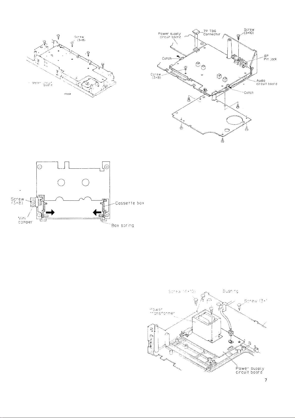
Meter Circuit Board
5. How to Remove the Cassette Door
(1 ) Remove the MINIthA'I'JIPER'retaining screw J x 8 CBTS(P)-
B and take out thé MINI DAMPER,
(2) Hold the legs of the CASSETTE BOX folded inwards and
pull up to remove the CASSETTE BOX and BOX SPRING.
tDN-730RI
Front surface of Front Ass'y
6. How to Remove the Audio Circuit Board
(1) Remove the top cover and the front panel. (Refer to section
. 1.)
Remove the front esc. ass'y. (Refer to section 2.)
(21
Remove the connectors from the audio circuit boaid and
(3)
power supply circuit board.
Side of the Side of the
Power supply CN901 — (7P) — CN901 audio circuit
circuit board TBG board
' CONNECTOR
Note: • Almost all of the service repairs to the audio cir
cuit board can be performed by removing the
bottom cover on the rear side of the chassis
Only when it IS unavoidable should you refer to
the removal method mentioned above.
• When reassembling, follow the procedures in
the reverse order. However, if each of the various
parts are not assembled properly in their respec
tive position, the sel cannot be assembled in
somie cases. Therefore, check the work of each
step carefully when assembling.
How to Remove the Power Supply Circuit Board
Remove the top cover and the front panel. (Refer to section
1 )
Remove the bushing that is fixing the power supply cord
from the chassis.
When the five screws (4x19 CBTS-P tight) (3x10
(3)
CBTS-P tight) that are holding the power transformer and
chicuit board are removed, the power supply circuit board
can be removed by raising it.
Cress.s
Remove the screw (3 x 10 CBTS-P tight) (3 xBCBTS-S
(4)
tight) that is holding down the 4P pin jack and circuit board.
By removing the two catches (left and right) of the chassis
holding down the circuit board in the directions of the
arrows shown below, the audio circuit board can be pulled
forward.
Page 8
IE)N-730ni
ADJUSTING AND CHECKING THE
MECHANISM SECTION
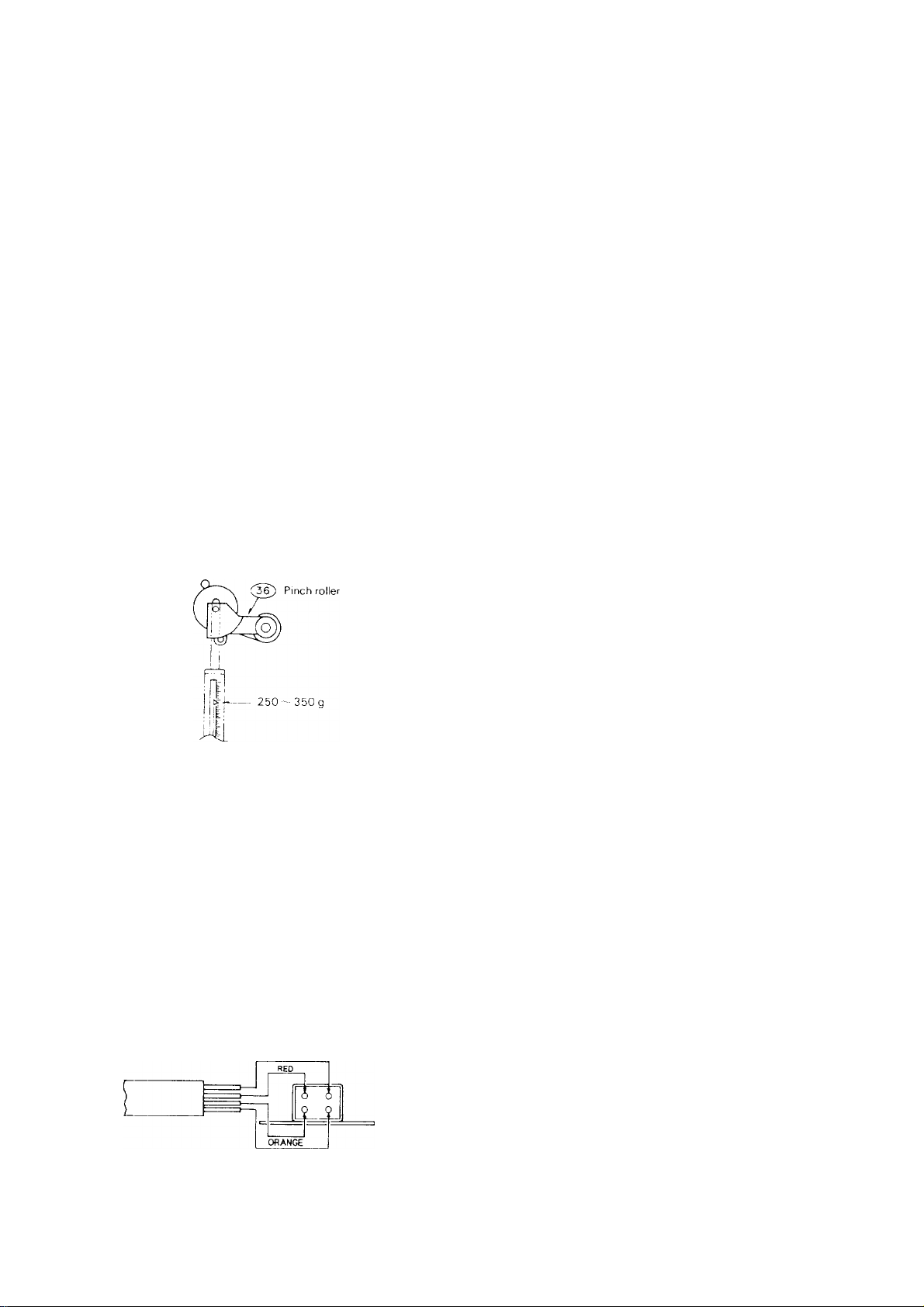
1. Replacing-the Pinch Roller (36)
Before replacing the pjnch roller, clean the tape contact surface
of the pinch roller and the capstan shaft.
Most causes of poor tape transport can be traced to dirty pinch
roller and capstan shaft. Remove the clips that press the pinch roller and pull the pinch
roller forward to remove it.
After replacing, run a padless C-90 tape to check for tape curls
at the tape guide section of the head.
2. Checking the Pressure Force of the Pinch
Roller (36).
In the playback mgdej^hpok a spring weight opto the bracket at
the center o* the pinch roller. After separating the pinch roller
from the capstan siTaft, allow the pinch roller to contact the caps
tan shaft again. Check to make sure the spring weight reads be
tween 250 ~ 350 g when the pinch roller starts to rotate
Replace the pinch roller (36) when it does not conform to the
standard specification values.
Capstan shaft
\
4. Replacing the ERASE HEAD (15)
(1) Unscrew the erase head holding screws (53).
(2) By unsoldering the HEAD W RES can be taken off the
mechanism unit.
(3) When the replacement is completed, secure the screws
with the screw lock.
white;
5. Checking the Take-up Torque
Load the cassette type torque meter (SONY TW21;1 1).
Check to make sure that the average torque meter reading is
within 30-70 g-crn during playback. If it is not within this range,
check the voltage (approx. 4V) of tha reel motor. If the voltage is
low, the torque will be weak: if it is high, the torque will be strong.
6. Checking the FF and REW Torques
Load the cassette type torque meter (SONY TW2231). Check to
make sure the torque meter indicates within 90—180 g-cm at
the end of FF and REW.
7. Checking the Back Tension Torque During
Record/Playback
Load the cassette type torque meter (SONY TW21 11) : check
to make sure the torque meter reads between 2 —6 g-cm during
playback and that there is no unevenness.
If it is not within this range, replace the reel ass'y (5) or Washer.
3. Replacing the Record/Playback Head (14)
(1) How to remove the R/P HEAD.
1) Remove securing screw (1) and azimuth adjusting
screw (1) from the record/playback head.
2) Remove the soldered head wire and disassemble the
mechanical unit to remove the record/playback head.
(2) How to assemble the R/P HEAD.
Reverse the above 1 procedures for removing the R/P
HEAD.
' Solder the HEAD WIRE according to the diagram,
mechanism (recording/play back head)
8. Checking the FF and REW Times
Load a C-60 cassette tape (DEMON GR-2/60): check to make
sure the tape is fast forwarded or rewound within 110 sec
onds. If it is not within this range, check sections 5 and 6.
9. Checking the Existence of a Cassette Housing and the Operation of the Erase Prevention, Metal and Chrome Switch
Confirm that the sensor arm properly detecting the tape t/pe de
tection holes on the cassette housina.
Page 9

DN-730RI
ADJUSTING AND CHECKING THE ELECTRICAL SECTION
e
Caution on adjusting
Before adjusting, clean the head surface, capstan and the
(1)
pinch roller with a gauze or a cotton swab moistened with
alcohol.
(2)
Demagnetize the R/P HEAD and the E. HEAD with a head
eraser
(3)
Completely demagnetize the adjustment screwdriver.
(4)
Unless instructed otherwise, set the various controls as fol
lows.
O INPUT volume
............................................................
maximum
O DOLBY NR switch................................................................OFF
O TAPE SPEED volume........................................Center position
1. Tape Transport Check
Load the transport check cassette. In the operational mode, illu
minate the fixing guides of the R/P HEAD with a lamp and check
to make sure the tape edge does not come in contact with the
tape guide section.
The tape transport is the most important element in determining
the performance of a cassette deck.
Avoid moving the various adjustment screws, nuts, etc., as much
as possible Refer to the pages on "Adjusting and Checking the
Mechanism Section" when replacing or adjusting the R/P HEAD.
3. Checking and Adjusting the Tape Speed
(1) Connect the frequency counter to the LINE OUT terminal
and load test tape (SONY TY-224).
(2) Playback a test tape. At about halfway through the tape,
where the tape transport is stable, adjust the adjustment
points (RT305) on the P.W. BOARD (222 2778 ♦**) so that
the frequency counter will have a reading within the
range of 3,000 Hz ±6 Hz. Fig. 3-1
F. Counter
PB Amp
LINE OUT
SONY TY-224
3000 I
3000 Hz
Í 6Hz
4. Adjusting the Playback and Recording
Section
Procedure Item
1 PLAYBACK
GAIN
2 P.B.
Frequency
REC/P.B.
3
Frequency
4
REC GAIN
REC/P.B.
5
Frequency
Usage tape —
input condition
A-BEX
TCC-130
A-BEX
TCC-162B,262B
GR-2/60
1 kHz, -40 dB
10 kHz, -40 dB
GR-2/60
1 kHz, -30 dB
GR-2/60
Dolby NR C
Response Mode
Fig. 4-1
Fig. 4-1
Fig. 4-2 REC. PLAY
Fig. 4-2 REC. PLAY
Fig. 4-3 REC. PLAY
PLAYBACK
PLAYBACK
1
PLAYBACK
1
PLAYBACK
i
PLAYBACK
Playback Fraquancy Raaponaa
Adjustment
iocation
RT-101 (L)
RT-201 (R)
RT-103 (L)
RT-203 (R)
RT-108 (L)
RT-208 (R)
Adjustment procedure
Adjust the LINEOUT output to 775 mV
(OdBs).
Make sure the playback characteristics
conform to Figure 4-2.
Record 1 kHz and 10 kHz alternately.
Adjust each volume so the 10 kHz
playback output is 0.5 dB in relation to
the 1 kHz playback output.
Adjust each volume to the playback output
is the same as when the recording monitor
is output.
Make sure that the DOLBY NR C recording
and playback characteristics conform to
Figure 4-3.
2.
Adjusting the Azimuth
After completing the tape transport check, load the test
(1)
tape (A-BEX TCC-153). Fig. 2-1
(2)
Playback the test tape; adjust the azimuth screw so that
section A of the resurge wave form is maximum and section
B is minimum. Fig. 2-2
OSCILLOSCOPE
RESURGE VYAVE
Y
O'
y
30'
Y
OK NG
O
90'
135'
180'
L-CM fl-CH
Fig. 3-1
Racord/Playback Ovarall Fraquancy Rasponsa
Tape HD-7E'60
Dolby NR Off
Level — 20 dB from Dolby Level
Dolby C Racord/Playback Ovarall Fraquancy Rasponsa
Fig. 4-1
Fig. 4-2
Fig. 4-3
Fig. 2-2
Page 10

I LJI\]- /LáUH I
EQUIPMENT FOR ADJUSTING AND CHECKING
MEASURING TAPE
II
TYPE NAME BRAND
TW-2111A/2121A SONY
TY-2231
GR-2/60 DENON
TCC-153 A-BEX
TY-224
TCC-130 A-BEX
TCC-162/262B A-BEX
TCC-902 A-BEX
2) MEASURING INSTRUMENT
Tension gauge
Audio signal generator
Variable resistance attenuator
Electronic voltmeter
Oscilloscope
Frequency counter
Adjustment screwdriver
Trap coil adjustment square stick
. TYPE NAME, BRAND AND USES
USES
Checking the Take-up Torque and
Back Tension.
SONY
Checking the FF and REW Torque
Checking the FF and REW Times.
Adjusting the Azimuth.
SONY
Checking and Adjusting the Tape
Speed.
Adjusting the Playback Level
Checking the Playback Frequency
Response
Transport checking cassette tape
NOTE FOR PARTS LIST
• Part indicated with the mark '' ® ” are not always in stock and possibly to take a long period of time for supplying, or in some
case supplying of part may be refused.
•When ordering of part, clearly indicate “1” and ‘T (i) to avoid mis-supplying.
• Ordering part without stating its part number can not be supplied.
• Part indicated with the mark is not illustrated inthe exploded view.
• Not including Carbon Film ±5%, 1/4W Type in the P.W.Board parts list. (Refer to the Schematic Diagram for those parts.)
WARNING:
Parts marked with this symbol A WBSS have critical characteristics.
Use ONLY replacement parts recommended by the manufacturer.
• Resistors
Ex.: RN
RD Carbon
Composition
RC
RS : Metal oxide film 2H . 1/2W
RW Winding
RN
. Metal film 3D 2W M
RK
Metal mixture
» Units; ohm
R 2
* Capacity (electrolyte only)
2 2 2
I ^
• Units: pF.
2 R 2 —
TL±
e Units: |iF.
14K
Type Shape Power Resist- Allowable Others
------------------
-----------------
2E 182 FR
and per
formance
2B 1/8W F
2E : 1/4W
3A . 1W K
3F
3H
1800 ohm “ 1.8 kohm
Indicates number of zeros after effective number
2-dlgit effective number.
-1,2 ohm
-1 -digit effective number.
-2-digit effective number, decimal point indicated by R.
2200pF
Indicates number of zeros after effective number,
- 2-digit effective number,
-2.2nF
-1 -digit effective number,
-2-digit effective number, decimal point indicated by R.
ance error
G
J ±5% NB . Non-burning type
3W
5W
1 formance | , 1
\
: ±1% P : Pulse-resistant type
±2%
NL : Low noise type
±10% FR Fuse-resistor
F
±20%
. Lead wire forming
• Capacitors
Ex.: ÇE 04W 1H ^ M ^
Type Shape Dielectric Capacity Allowable Others
1 and per- strength error
i I 1
CE . Aluminum (Oil
electrolytic
CA : Aluminum solid
electrolytic
CS : Tantalm electrolitic
Film
CO
CK
. Ceramic IV
CC . Ceramic 1H 50V
CP
Oil 2A 100V
CM ; Mica
CF
Meiaiized
CH
. Meiaiized
OJ
1A
1C : 16V J ±5% HR : Ripple-resistant type
IE 25V K
2B 125V P
2C 160 V
2D 200V
2E 250V D
2H
2J
* Capacity (except electrolyte)
2 2 2
-------------- 2200tiMF - 0.0022pF
I ^— (More than 2) — Indicates number of zeros after effective number.
^
------------------------------
e Units: pF
2 2 1
---------------
l—(0 or 1)
T
-----------------------------
• Units. PF.
a When the dielectric strength is indicated in AC. “AC" is included after the
dielectric strength value.
220PF
----------------
F
:6 3V
10V
35V
; 500V
630V
±1%
HS : High stability type
G . ±2% BP
: ±10% DL : For charge and discharge
M
±20% HF : For assuring high
Z : +80%
-20%
+ 100% W UL-CSA type
-0%
+025pF
C
±0.5pF
-
: Others
• Non-polar type
frequency
U : UL part
C : CSA part
F
. Lead wire foming
2-digit effective number.
Indicates number of zeros after effective number.
2-digit effective number
10
Page 11

□N-730R
PARTS LIST OF GU-2778 AUDIO/METER UNIT
■< Ref. No.
1 Part No.
SEMICONDUCTORS GROUP
IC301
iC3o;:
j
IC303
1C304
1C306
IC307
■ IC501 '
'lC601
i 1СЭ02
1 1СЭ03
IC309
IC602
1СЭ01
IC9C4
IC910, 911
TRI 01
TR102
TR103
TR104
TRIOS, 109
TR111~113
TR114, 115
TR201
TR202
TR203
TR204
TR208, 209
TR211-213
TR'307
TR.308
TR309, 310
TR370
TR371
TR507
TR508
TR515
TR552, 553
~P554~556
TF 557
TR558
TR559
TR560, 561
TR601
TH904
' DI55
D255
D315, 316
D320
D503
D517, 518
D553
D554
D601,602
D901~904
СЭ10, 911
C915, 916
ZD304, 305
ZD410
2D531
2D551
ZD552
¿:D907
I ZD912
ZD913
i
_
262 0590 001
1 262 08&ÌÌ106
263 0720 Ó04 _
263 C565 007
¡ 263 0711 000
1 263 0354 001
263 0565 007
! 262 0447 009
1 222 2045 001
1
262 1711 909
1 263 0810 008
I 263 0503 001
263 0793 002
263 3432 907
268 0072 003 ICJ’rotector ICP-NIO
269 0074‘*907’'|Trarrsistcir DTA114TS(10K) ^ Built in Resistor
269 0102 905 Transistor DTC124EKT146 Built in Resistor
273 024S900 | Transistor 2SC2603E/F T [
275 0048 912 ! Transistor 2SK381 (B)/(C)-T j
269 0038 906
____
269 0088 906
269 0102 905 I Transistor DTC124EKT146- | Built in Resistor
269 0074 907 ] Transistor DTAl 14TS(1 OK) j Built in Resistor
269 0102 905 Transistor DTCl 24EKT146 Built in Resistor
273 0245 900 i Trans stor 2SC2603E/F T |
275 0048 912 i Transistor 2SK381 (B)/(C)-T |
269 0088 906 ! Transistor DTCl 14TKT96 ; Built in Resistor
269 0088 906 I Transistor DTCl 14TKT96 | Built in Resistor
265 0040 902 j Transistor DTC144ES(47K-47K) 1 Built m Resistor
272 0025 907 j Transistor 2SB562iC)TF
273 0245 900 , Transistor 2SC2603E/F T
I 269 0018 905
! 269 0022 904
269 0062 906 ' Transistor DTC124E5(22K-22K) Built in Resistor
269 0016 907 i Transistor DTA144WS(47K-22K) Built in Resistor
269 0018 905 I TransistO' DTC143ES[4.7K-4.7K) Built in Resistor
269 0091 906 ^ Transistor DTC143TKT96 ' Built in Resistor
274 Q03B 905 ; Transistor 2SD468[C)TF j
269 0015 908 Transistor DTC124XS(22K-47K) | Built in Resistor
269 0082 902 I Transistor DTCl 14EKT96 ! Built in Resistor
269 0054 901 Transistor DTC144EKT96 , Built in Resistor
271 C183 92-7 ■ Transistor 2SA933(R/S)T93 i
269 C122 901 ‘ Transistor DTC144WKT146 | Built in Resistor
272 0025 907 '
276 0432 903 ¡
276 0432 903
276 0432 903
276 0432 903
, 2>
_ ’6 0432 903 i Diode 1 SS270A TE |
■ 2
276 0553 905 i Diode 1 SR35-200A{T93X) '
276 0432 903 : Diode 1SS270A TE j
276 0432 903 | Diode 1SS270A TE |
276 0553 905 I Diode 1 SR35-200A(T93X) |
2 76 0553 905 ' Diode 1SR35-200A(T93X) i
Transistor DTC114TKT96 | Built in Resistor
^6 0553 905 i Diode 1 SR35-200A(T93X) |
Part Name
TCUPC1330HA
1C UPG4570C 1C HA12170NT
1C BA15218
1C M5218AP
1C UPC1297CA
1C BAI 5218
1C BA6109U1
^ Computer UPD78043GF-
100-3B9
IC X24C00S
1C NJM7808FA(S)
IC NJM7908FA
IC NJM7806FA(S)
IC NJM78L05AT
Transistor DTC114TKT96 ! Built in Resistor
I
Transistor DTC143ES(4.7K'4.7K) Built in Resistor
Transistor DTA143ES(4.7K-4.7K) Built in Resistor
Transistor 2SB562(C)TF .
Diode 1SS270A TE
Diode 1SS270ATE |
Dioce 1SS270ATE
Diode 1SS270ATE |
Diode 1SR35-200A{T93X}
Zener Diode HZS9B-1TD
Zener Diode HZS9B-1TD
Zener Diode HZS9B-1TD
Zener Diode HZS4C-1TD
Zener Diode HZS7B-1TD |
Zener Diode HZS6C-1TD
Zener Diode HZS27-1TD
Zener Diode HZS11C-1TD
i
i
j
Remarks
Ref. No.
RESISTORS GROUP
(not included Carbon Film ±
VR101
i
VR103
VR108
VR201
VR203
VR208
VR301
VR304
VP305
R101, 102
R103
R104
R105
R108
R41
R112
R118
R120
RI32
R135
R140
R141
R142
R143
R144
R145
R150
R151
AR152
R156
R160
L
R161
FÌ162
R163
R164
R175
R177
R173
RISO
RISI
RI 89
R199
R201, 202
R203
R204
R205
R208
R212
R218
R220
R229
R232
R235
R240
R241
R242
R243
R244
R245
R250
R251
Part No.
211 6093 967
211 6093 970
211 6093 954
211 6093 967
211 6093 970
211 6093 954
211 0707 000
211 0835 008
211 6093 912
247 0010 987
247 0005 947
247 0010 974
247 0014 912
247 0014 967
247 0008 960
247 0009 ÍM3
247 0009 985
247 0010 929
247 0006 962
247 0007 '945
247 0011 986
247 001 1 944
247 0012 927
247 0010 929
247 ООП 902
247 0005 905
247 0012 969
247 0010 929
‘241 2315 912
247 0005 905
247 0010 961
247 0012 927
247 0010 961
247 0006 988
247 0006 975
247 0014 967
247 0007 974
247 0009 914
247 0009 901
247 0008 902
247 0017 906
247 0010 974
247 0010 987
247 0005 947
247 0010 974
247 0C14 912
247 0014 967
247 0009 943
247 0009 985
247 0010 929
247 0009 956
247 0006 962
247 0007 945
247 0011 986
247 ООП 944
247 0012 927
247 001 о 929
247 0011 902
247 0005 905
247 0012 969
i 247 001 о 929
Part Nam6:
-5% 1/4 W type)
Adjust 47K ohm
Adjust 100K ohm
Adjust 22K ohm
Adjust 47K ohm
Adjust 100K ohm
Adjust 22K cihrn
Valiable 100K ohm (INPUT)
Valiable 5K ohm
Adiust 4.7K ohm
Ch p 27K ohm
Ch.p 150 ohm
Chip 24K ohm
Chip 620K ohm
Chip IM ohm
Chip 3.3K ohm
Chip 6.3K ohm
ChiplOKohrr
Chip 15K ohrr
Chip 470 ohm
Chip IK ohm
Chip 68K ohiTi
Chip 47K Ohm
Chip 100K ohm
Chip 15K ohm
Chip 33K ohm
Chip 100 ohni
Chip 150K ohm
Cnip 15K ohm
Carbon Him 10 ohm 1/4W
¡Fusible) ; . uuh
Chip 100 ohn
Chip 22K ohm
Chip 100K ohm
Chip 22K ohm
Chip 560 ohm
Chip 510 ohrn
Chip ’ M chn
Cihip 1,3K ot m
Chip 5.1 К ohm
Chip 4.7K ohm
Chip 1,8K ohm
j Chip lOM ohm
j Chip 24K ohm
Chip 27K ohm
Chip 150 ohm
Chip 24K oh m
Chip 620K C'hrr
Chip IM ohm
i Chip 6.SK ohmi
i Chip lOK ohm
Chip 15K ohm
Chip 7.5K ohm
i Chip 470 ohm
Chip IK ohm
Chip 68K oim
Chip 47K onm
Chip 100K ohn
Chip 15K ohm
Chip 33K ohm
Chip 100 onm
Chip 150K ohm
Chip 15K chrr
Remarks
V06PB473T
V06PB104T
V06PB223T
V06PB473T
V06PB104T
V06PB223T
V09V25FA104. i
V16V25Í-B502MG
1
V06PB472T
I
RM73B-273JT
I RM73B-U51JT I
RM73B--243JT '
I RM73B-624.T !
I RM73B--105.T ;
RM73B--332JT '
I RM73B-6S2JT i
RM73B-103JT
RM73B-153JT
RM73B-.471.it
RM73B-102.JT '
RM73B-683.JT
RM73B-473JT
RM73B-104JT
RM73B-153JT
RM73B-333JT
RM73B-101JT
RM73B-154JT
RM73B-153JT
RD14B2E100GFnST
-101JT
RM73B
-223JT
RM73B-
104JT
RM733-
■223JT
RM73B-
-561JT
RM73B-
-51IJT
RM73B
105JT
RM73B-
-132JT
RM73B
■-512JT
RM73B-
-472JT
RM73B-
-182JT
RM73B-
-106KT
RM73B-
-243JT
RM73B-
-273JT
RM73B-
-1E4JT
RM73B-
-243JT
RM73B-
-624JT
RM73B
-105JT
! RM73B-
-682JT
RM7 3B
--103JT
RM73B
-153JT
RM73B
--752JT
j
RM73B-
-471JT
RM73B-
-102JT
; RM73B-
■633JT
j
RM73B-
--473JT
1 RM73B-
-104JT
j RM73B
-153JT
RM73B
-333JT
RM73B-
-101JT
i RM73B-
-154JT
RM73B
-153JT
RM73B-
j
j
j
i
11
Page 12

IDN-‘730R I
Ref. No.
r-7 - -■'
fáSR25:
: R253
i R256
Í
R257
1 R260
I
R261
' R262
R263
' R280
R289
R299
, R301
■ R321
R330
R331
, R332
' R334
R336, 337
R360, 361
R36¿*363 .
R364
R365
R370. 371
R401,402
, R403
R404
R405
R406
: R501-506
■ R507
: - R508
R510, 511
R513, 514
^ R516
R518
R520, 521
R540
R556
R557
R558
R559
R560
R561
R562
1
а \ н5б з у
R564. 565
- R571
R573 : 247 0009 956 1 Chip 7.5K ohm
R574 : 247 0009 985 | Chip 10K ohm
R577-580 ^ 247 0012 927 ' Chip 100K ohm
R581 ; 247 0012 927 Chip 100K ohm
R602 247 0010 916 ChipISKchm
R603, 604 247 0007 945 i Chip IK ohm
R605. 606 247 0012 927 ' Chip 100K ohm
R610. 611 I 247 0007 945 | Chip 1К ohm
R612 i 247 0007 945 | Chip IK ohm
R613 247 0009 985 | Chip 10K ohm
R650 247 0005 947 : Chip 150 ohm
R652 247 0005 963 | Chip 180 ohm
R654 .247 0006 917
R660 , 247 0005 947
R662 247 0005 963
R664 247 0006 917
R666 247 0006 956
R670 247 0005 947
R672 247 0005 963
R674 247 0006 917
R676 j 247 0006 959
■ Part No.
241-2315 912
247 0009 aS5
247 0005 905
241 ТЮ14 907
'247 001СГ 961
247 0012 927
247 0010 961
247 0006 988
247 0008 944
247 0017 906
247 0010 974
247 0010 961
247 0010 945
247 0009 985
247 0009 901
241 0007 987
, 247 0007 961
j 247 0008 así
: 247 0012 943 1
1 241 2815 925'!
247 0009 901
247 0009 985
247 0001 983 ;
247 0012 943
1 247 0012 Э27
24.7 0005 989
, 247 0004 922
' 247 0012 927
247 001 2 927
247 0011 944
247 0015 940
( 247 0011 944
1 247 0012 927
247 0018 905
1 247 0009 985
; 247 0009 985
' 247 0009 985
247 0010 961
247 0009 985
247 0010 961
247 0009 985
247 0007 945
244 2055 970
247 0007 987
1 241 2з!?912
247 0009 985
247 0018 905
Chip 10K ohm
Chip 100 ohm
Chip 1M ohm
Chip 22K ohm
Chip TOOK ohm
Chip 22K ohm
Chip 560 ohm
Chip 2.7K ohm
Chip 10M ohm
Chip 24K ohm
Chip 22K ohm
Chip 18K ohm
Chip 10K ohm
Chip 4.7K ohm
Chip 1.5K ohm
Chip 1,2K ohm
Chip-3Kohm >
Chip 120K ohm
Carimn Film 22 ohm 1/4W (Fusible)
Chip 120K ohm
Cnip 100K ohm
Chip 220 ohm
Chip 47 ohm
Chip 100K ohm
Chip 100K ohm
Chip 47K ohm
Chip 2.2M ohm
Chip 47K ohm
Chip 100K ohm
Chip 0 ohm
Chip 10K ohm
Chip 10K ohm
Chip 10K ohm
Chip 22 ohm
Chip 10K ohm
Chip 22K ohm
Part Name
Chip 300 ohm
Chip 150 ohm
Chip 180 ohm
Chip 300 ohm
Chip 430 ohm
Chip 150 ohm
Chip 180 ohm
Chip 300 ohm
Chip 430 ohm
Remarks !
RD14B2E100GFRSt|
RM73B-103JT
RM73B-101JT
RM73B-105JT
RM73B-223JT
RM73B-104JT
RM73B-223JT
RM73B-561JT
RM73B-272JT
RM73B-106KT
RM73B-243JT
RM73B-223JT I
RM73B-183JT i
RM73B-103JT I
RM73B-472JT I
RM73B-152JT
RM73B-122JT
RM73B-302JT
RM73B-124JT j
RD14B2E220GFRST |
RM73B- 472JT
RV173B--103JT
RM73B--4R7KT
RM73B-124JT
RM73B-104JT
RM73B--221JT
RM73B-470JT
RM73B-104JT
RM733-104JT
RM73B-473JT
RM73B-225JT
RM738-473JT
RM73B-104JT
j RM73B-0R0KT
RM73B-103JT
RM733-103JT
RM73B-103JT
RM73B-223JT
! RM73B-103JT
RM73B--223JT
RM73B--103JT
RM73B-102JT
RSi4B3A560JST(s:i
RM73B-152JT
I RD14B2E100GFRST
RM75B-103JT
RM73B-OROKT
RM73B-752JT
RM73B-103JT
RM73B--104JT
RM73B-104JT
RM73B'-133JT
RM73B--102JT
RM73B-104JT
! RM73B-102JT
RM73B-102JT
RM73B-103JT
RM73B-151JT
RM73B-181JT
RM73B-301JT
RM73B-151JT
RM73B-181JT
RM73B'-301JT
RIV173B-431JT
RM73B-151JT
RM73B-181JT
RM73B-301JT
RM73B-431JT
Ref. No.
Part No.
_L
CAPACITORS GROUP
C101
Cl 03
Cl 09
Cl 27
C142
C150
C151
C152
Cl 53
C154
Cl 55
C201
C203
C209
C227
C242
C250
C251
C252
C253
C254
C255
C350 ■
C352
C353
C354
C355
C356
C402
C403
C501-504
C506
C507
С50Э, 510
C512, 513
C515, 516
C517
C551, 552
C553
C554
C555
C601-603
C6Ü4
C902, 903
C906, 907
C908
C910
СЭ11
C913
C918
R126
R169
R226
R269
257 0008 996
257 0009 979
257 0009 937
257 0005 902
257 0005 944 i
257 0008 996
257 0010 900
257 0004 961
253 1131 909
257 0011 967
257 0010 942
257 0008 996
257 0009 979
257 0009 937
; 257 0005 902
¡ 257 0005 944
I
257 0008 996
257 0010 900
257 0004 961
j 253 1131 909
i 257 0011 967
; 257 0010 942'
I 257 0013 907
I 257 0002 921
I
257 C009 940
257 0009 940
257 0010 900
! 257 0009 995
I 257 0002 92"
j 257 0014 935
■ 257 0008 983
257 0008 983
257 0008 983
257 0010 900
I 257 0008 983
! 257 0008 983
257 0013 910
. 257 0010 900
^ 257 0011 941
257 0010 900
254 4403 71 3
i 257 0008 983
257 1013 977
i 254 4403 713
257 0013 910
254 4403 721
254 4250 796
257 0Ü13 910
25^1 4414 707
257 0013 910
257 0008 983
257 0008 967
257 0008 983
257 0008 967
OTHER PARTS
LlOl
LI 03
LI 04
L105
L201
L203
L204
L205
L301
232 0109 003
235 0020 945
235 0020 916
239 0010 009
232 0109 003
235 0020 945
235 0020 916
239 0010 009
231 0078 005
Part Name
Chip (Cerarnici 0.0012 |iF/50 V
Chip (Ceramic) 0.0056 ¡iF/SOV
Chip (Ceramic) 0.0027 u.F/50 V
Chip (Ceram c) 150 pF/50 V
Chip (Ceram, c) 220 pF/50 V
Chip (Ceramic) 0.0012 pF/50 V
Chip (Ceramic) 0,01 pF/50 V
Chip (Ceram c) 100 pF/50 V (
Ceramic 390 pF/500 V i
Chip (Ceramic] 0,033 pF/25 V |
Chip (Ceramic) 0.022 pF/50 V 1
Chip (Ceramic) 0.0012 u.F/50 V j
Chip (Ceramic) 0.0G56 pF/50 V i
Chip (Cera Tiic) 0.0C27 pF/50 V i
Chip tCeramic) 1 50 pF/50 V
Chip iCeramic) 220 pF/50 V-^
Chip [Ceramic 0.0012 uF/50 У -|
Chip (Ceramic) 0,01 u.F/50 V !
Chip (Ceramic) 100 pF/50 V i
Ceramic ЗЭС pF/500V '
Chip (Cerarnici 0.033 uF/25 V (
Chip (Cerarnici 0.022 uF/50 У !
Chip (Ceramic) 0.047 uF/50 У
Chip (Ceran'ic) 10 pF/50 V
Chip (Ceramic) 0,0033 pF/'50 У i
Chip (Ceramic) 0.0033 uF/50 V ;
Chip (Cerarr ic) 0.01 uF/50 V i
Chip (Ceramic} 0.0082 |iF/50 V
Chip (Ce'ariic) 10 pF/50 V j
Chip (Ce'arriic) C.l jiF/50 V '
Chip (Ceramic) 0.001 uF/50 У
Chip {Ceramic) 0.001 uF/50 V
Chip (Ceramic) 0.001 pF/50 V
Chip (Ceramic) 0.01 uF/50 V
Chip (Cera.mi:) 0.001 uF/50 V
I Chip (Ceramic) 0.001 uF/50 V
j Cnip (Ceriimic i 0,058 uF/50V
: Chip iCeramic') 0.01 uF/50 У
1 Chip iCeram.iC) C.022 uF/25 V
j Chip iCera.micl 0 01 uF.'OO V
i Electrolvtic 1000 pF/25 V
Chip ■Ceramic) O.ODl pF/50 У
Chip (Ceramic) 0.C68 uF/50 V
Electrol\tic 1000 pF/25 V
Chip ;Cer smic) 0.068 uF/50 V
' Electralytic 2200 uF/25 V
I Electrolytic 4700 uF/6.3 V
; Chip (Ceramy) 0.C58 i.iF/50 V
Electrolytic 470 uE/50 V
■ Chip (Ceram:) 0.068 uF/50 V
j Chip (Cetamie) 0,001 uF/50 У
I Chip iCerarnic) 380 pF/50 V
I
Chip (Ceramm) 0 001 pF/50 V
I Chip iCeramic) 680 pF/50 V
МРХ Filter
Inductor 163JT
Inductor 8:¿2JT
HX Step up coi
MPX Filter
Inducto' 153JT
Inducto' 822JT
HX Step u|) coil
OSC Coil j
Remarks
CC73SL-H122JT
CK73B1H562KT
CK73B1H272KT
CC73SL1H151JT
CC73SL1H221JT
CK73B1H122KT
CK73B1H103KT i
CC73SL1H101JT I
CK45B2H391KT |
CK73B1E333KT
CK73B1H223KT
CC73SLIH122JT
СК73В1Ч562КТ
CK73B1 H272KT
CC73SL1H151JT
CC73SL1H151JT
CK73B1H122KT
CK73B1H103KT
CC73SL1H101JT
CK45B2H391KT
CK73B1E333KT
CK73B1H223KT
CK73B1H473ZT
CC73SL1H100DT
CK73B1H332KT
CK73B1H332KT
CK73B1H103KT
! CK73B1H822KT
I
CC73SL1H100DT
CK73F1E104ZT
CK73B1H102KT
CC73B1H102KT
CK73B1H102KT
; CK73B1H103KT
CK73B1H102KT
CK73B1H102KT
c:<73B’ H683ZT
C<73B'H103KT
C<73B'E223KT
C<73B‘ H103KT
ci;04vv'ii02Mc;sMG
CK73B1H102KT
CK73B1H683KT
C::04 VV1 E10 2:> .1C S: \1G
CK73BIH683ZT
CE04 W1E 222M CS MG
CE04 WOJ4 72 MC iSMCl
CK73BIH683ZT
CE04 W1H 471M CSM G
CK73B1H683ZT
CK73B1H102KT
CK73B1H681KT
CK73B1H102KT
; CK73B1H681KT
I
12
Page 13

Re1. No.
XT501
FL601
SW610, 612,
614,
620, 622,
624,
628, 630,
632. 634,
636, 638,
JK301 204 8261 003
JK302 : 204 8264 026 Head phone Jack
JK303 204 8416 007 Mini Jack
CN121 ; 205 0880 003 23P FFC Connector Base
CN122 i 205 0343 061 6P Connector Base (KR-PH)
CN131
CN141 ■ 205 0343 049 4P Connector Base (KR-PH)
CN191 205 0711 075 7P TBG Connector Base
CN301
CN302 i 205 0:i43 032 3P Connector Base (KR-PH)
W122 ! 204 0265TI78 6P KR-DA Connector Cord
W131
W141
W151 204 2326 009
WÌ51 1 203 6236 066 4P KR'DA Connector Cord
W252
WARNING:
• Pans marked with .T;, and/or shading have special characteristics important
to safety.
Be sure to use the specified parts for replacement.
Part No.
399 0107 007
393 8002 009
212 5604 910
616,
626,
205 0343 032 3P Connector Base (KR-PH)
, 205 03143-05^.
j 203 4753 046
! 203 6374 025 4P KR'DA Connector Cord
' 203 8216 042 5P KR-DA Connector Cord
Part Name
Ceramic Oscillator
£L Tube
Tact Switch
4P Pin Jack
Connector Base (KR-PH)^,
3P KR-DA Connector Cord
7P KR-DA Connector Cord
CTS4.19MGW
F1P6BGM6
LINE IN, OUT
HEAD PHONE
CD SYNCRO.
Remarks
iDN-yaOR
PARTS LIST OF 3U-2603 POWER SUPPLY UNIT
Ref. No.
SW901
CN191
CN901
ii' C901
4^' ' .
h F901
.'îi
WARNING:
• Parts marked
to safety.
Part No. Part Narne
212 0286 003
205 0711 075
205 0581 001
253 8014 702
445 0056 008
206 2089 009
206 2123 009
206 2110 004
206 7088 000
■
233 5985 005
233 5758 009
233 5760 000
206 1031 045
202 0022 0C3
212 4698 008-
with
Power Switch
7P TBG Connector Base
2P VH Connector Base
Ceramic Capacitorff.Ci‘uF/400VAC
Cord Bush ' ; ' ' iXt} i
AC Cord With Connector-M;
AC Coni Wilh Connector’.^AC Cord With Connector'^'j
AC Cord Wi»h Connector, **
Power Transforncr r }■
Power Trans .
P.jwer Tr.i'is'oinor ‘
Fuso 10 25'A
I Fuse Holder . - " 3^-^
j Voltage Selecioi (D)
and/or shading have special characteristics important
For AC Core
CK45f2GAC103MC
USA Canada^’r";
Multi-Voltage '
I Multi-Voltage Only
I Multi-Voltage Only
|MiHl^Voltage Only
Remarks
13
Page 14

l[DN--y30RI
PARTS LIST OF EXPLODED VIEW
Ref. No.
• 1
•; 2
•) 3
4
Í. 5
.Í,
A .
A 6 ,
A 1 "
A
A-
A -
A 8
• 9
• n
12
. 13
, 13-1
, 13*2
* 13-3
• 13-4
. 14
15
16
18
19
21
22
- 23
25 431 0310 046
26
27 113 1436 393
28 113 1480 255
29 113 1438 045
30
31
• 32
* 33
• 34
35 103 1511 318 CASSETTE BOX
36
37 463 Ò659 018 BOX SPRING [R)
38 103 1660 007
39
• 40 414 0595 015
• 41 203 2279 014 2C TERMINAL WIRE 3T
• 45 102 0434 419
• 46 473 8047 001 SPECIAL SCREW
• 47 412 3676 207 EJECT LEVER
• 48
• 49 463 8238 004 SPRING
• 50
• 51
• 53
* 54 412 3942 009 VOLUME BRACKET
101 473 7508 017 3 X 10 CBTS(P)-B
102
103
104
105 473 7500 044 3X8 CBTS(P)-B
106 473 7002 018 3X8 C8TS(S)-Z
107
108
■ Part No.
411 1000 652 CHASSIS
411 1000 681
411.1000 665 CHASSIS
412 2523 115
105 0787*107
338 0168 009 CASSETTE MECHANISM
■'233'^'5«)5'
233 5758 009
233 5760 000
CHASSIS
EARTH BRACKET
BOTTOM COVER
^ER'TRANSFORMER ’' Europe, U.K, .
POWER TRANSFORMER -
POWER TRANSFORMER
212 0286 003 POWER SWITCH . , •
206 2089 106 i AC CORD WITH CONNECTOR J
206 2128 009 AC CORD WITH CONNECTOR
206 2110 004
AC CORO WITH CONNECTOR. ’ ■
206 2088 000 AC CORD WITH CONNECTOR ' '
445 0056 008
412 2008 012 BUSHING PLATE
414 0637 009 SHIELD LABEL
104 020a2-U^ FOOT ASS’Y 1.
GU-2778
—
— METER P.W.B.
— H/P JACK P.W.B.
3U-2603
205 0712 074
204 8261 003 4P PIN JACK
211 0707 000
412 3951 003
211 0835 008
204 8264 026 HEAD PHONE JACK
393 8002 009 EL TUBE (FIP6BGM6)
113 1481 364 PUSH KNOB (B)
112 0515 173 VOLUME KNOB
112 0727 042 VOLUME KNOB (C)
103 1650 101
143 0765 215 METER WINDOW
144 2309 216
463 0655 009 CASSETTE SPRING
421 9007 007 MINI DAMPER
412 3628 006
412 3677 015
445 8028 009 CORD HOLDER
513 2150 001 WARNING SHEET
477 0262 006 SPECIAL SCREW
473 7502 013 4 X 10 CBTS(P)-Z
473 7509 058 4X12 CBTS(P)-B
473 7007 039
471 3102 013 2 X 5 CBS-Z
CORD BUSH , , •
AUDIO/METER P.W.B UNIT
AUDIO P.W.B.
VARI PITCH P.W.B,
POWER TRANS P.W.B. UNIT
7P TBG-S CONNECTOR
VARIABLE RESISTOR 100K
REFLECTOR
VARIABLE RESISTOR 5K
POWER SWITCH LEVER
ASS'Y
FUNCTION KEY
PUSH KNOB (A)
EJECT KNOB
FRONT ESCUTCHEON ASSY iTK)
FRONT PANEL
CASSEHE WINDOW lA) ASS'Y
EARTH PLATE
TOP COVER
LEVER STAY (B|
MOUNT BRACKET
4 X 20 CBTS(S)-B
Part Name
Remarks
Europe, U.K.
U.S.A., Canada
Multi-Voltage
U.S.A., Canaria ,
Multi-Voltage
(SW001) ' ' ■
Europe
U.K.
U.S.A., Canada '
Multi-Voltage 7. »•
(jK3oi:
V0920V25FA104
V1620V35FA502 (MG)
(FL601)
WARNING:
• Parts marked with
to safety.
Be sure to use the specified parts for replacement.
• Part indicated with the mark are not always in stock and possibly to take a
long period of time for supplying, or in some case supplying of part may be
refused.
and/or shading have special characteristics Important
14
Page 15

EXPLODED VIEW
IDN-730RI
ao4).._
WARNING:
Parts marked with this symbol A EM have critical characteristics.
Use ONLY replacement parts recommended by the manufacturer.
D
15
Page 16

IUN-‘/3aRI
EXPLODED VIEW OF CASSETTE MECHANISM
16
Page 17

I DN-73DRI
PARTS LIST OF CASSETTE MECHANISM EXPLODED
VIEW
Ref. No.
2
3
4
5
6
7
8
10
11
12
13
14
15
16
») 17
18
19
20
21
24
25
26
27
28
29
30
31
32
33
34
36
38
39
40
41
42
43
44
51
52
53
54
Part No.
9DF 5170 49
9DF 5642 85
9DF 6121 51
9DF 6230 37
9DF G156 11A
9DF Jill 17
9DU J12V 11
9DF C52E 47
9DF K26N 14
9DF D45T 17
9DF U192 11
9DF U18K 12
9DF K21U 11
9DF 5252 56
9DF 5673 52
9DAW13G 00
9DU E16E 11
9DF C39S 33
9DF C52H 12
9DF D45G 21
9DF D45B 16
9DF D44T 14
9DF D44Y 12
9DF D44V 12
9DF F17W31
9DF J111 30
9DF Jill 14
9DF K28M 12
9DF K28R 11
9DF R22H 11
9DF R20L 22
9DF G114 14
9DF G15S 11A
9DU G13U 15
9DU G20B 11
9DF 7652 63
9DF L39H 12A
9DF L39K 12
9DW H63P 05
9DW H55L 05A
9DF G137 18
9DF F17C 12
Part Name
IDLER
REEL MOTOR
CHASSIS BASE
REEL BASE
SCREW 2.6 X 6.4 ZN
WASHER 1.7 X 0.25T
POLY WASHER 2.1 X 0.25T
HEAD BASE
HB SPRING
HEAD SPACER
ERASE HEAD
R/P HEAD
SPRING
MAIN MOTOR
CONTROL P.W.B. Ass'y
REEL SENSOR (GP2S04B)
PUSH SWITCH
EJECT PROTECT ARM
CASSETTE SPRING
PLAY ARM
CAM GEAR (3R)
REC. SENSOR LEVER
PACK SENSOR LEVER
METAL SENSOR LEVER
MAIN BELT
POLY WASHER 2.6 X 0.25T
POLY WASHER 2.6 X 0.5T
EJECT PROTECT SPRING
SLIDE SPRING
FLYWHEEL Ass'y
PINCH ROLLER Ass'y (R)
SCREW 2.6 X 5 ZN
SCREW WITH STEP (7.7)
E RING
WAVE SCREW 3 X 8 ZN
SOLENOID
IRON CORE
PLUNGER
ERASE HEAD CORD
R/P HEAD CORD
2 X 9F LOCK SCREW
HOLDER CUSHION
Remarks
PARTS LIST OF PACKING & ACCESSORIES
Ref. No. Part No. Part Name Remarks Q'ty
1 505 8092 007 LAMINATE ENVELOPE FOR SET 1
3
4 501 1698 037
5 505 0038 030 POLY COVER
6
7 399 0250 006
8
9 203 4880 003
10 515 0692 004 DEL WARRANTY COM U.S.A. Only 1
11 502 0852 000
m ^
WARNING:
• Parts marked with ^ and/or shading have special characteristics important
to safety.
Be sure to use the specified parts for replacement.
503 1079 005 CUSHION 2
501 1853 005
511 2682 007 INST. MANUAL (5) 1
203 2360 004 2P PIN CORD 2
CARTON CASE 1
CARTON CASE U.K. 1
REMOTE UNIT (RC^I) 1
3P MINI PLUG CORD 1
PAD ASS'Y
U.K. Only
PACKING & ACCESSORIES
1
1
17
Page 18

lUN- 73GHI
ì P.W. BOARD OF GU-2778 AUDIO/METER UNIT
D
18
Page 19

P.W. BOARD OF 3U-2603 POWER SUPPLY UNIT
IDN-730RI
Remarks
1. The following table shows the power circuit parts used for the 3U-2603 board by area.
2. Parts used are marked O, parts not used —.
Ref.No.
Areas
Europe (E2)
U.K. (EK)
Multi-Voltage (E1)
U.S.A. & Canada (E3)
Power T rans
part No.
2335985005
2335760000
2335758009
Voltage
Selector
- -
— -
O
-
FUSE
F901
O
-
JV901
o
o
--
o
JV904 JV905 JV908
JV903
- -
o
-
o
O
-
-
o
-
-
- -
-
-
O
19
Page 20

IDN-TSORI
SEMICONDUCTORS
• 1C
M15218AP
|.iPC4570C
TL4558
3 GND
2 INPUT
1 OUTPUT
• NJM7908
3 INPUT
2 GND
1 OUTPUT
• NJM7808
• NJM7806
20
/LtPC1330HA
Page 21

^ 2
Q P,
<
g
H
fO ro _
с
<<O
M O
<
O
X
O
Z
о
< с
< N Н
Г О -, —
СЛ СЛ
J3 СЛ
w M
X X X X I
rsi N fSI N1 NJ
СЛ СЛ (Л СЛ СЛ
<D 0> 0> 05
Ш 9 ro n О
NJ CO
X X X X
N1 N1 N rsl
СЛ СЛ (/) СЛ
CO Ю -»
ro Ш ^
PO M ^
• •
о о
H -I
n о
11
m <
о
5’
Q.
(D
(Л
со PO —‘
О ГО
О ш
— v>
Q)
3
3
w
rô
O
-Ч
t/l
t
О Q
Н Н
> >
1
• • • •
о о о о
н н н н
о о о о
^ ^ PO PO
''Р
• •
О о
-I н
о о
со -с>.
7^ X
5
1
■:5
гЛ
со 4^ .1^
m m >< m
(Л (/> (Л (Л
O
—<
O
'^O
СЛ СЛ
O ro
^ en
05 05
00 M
ri
00
c
g
>
O
J3
>
L .J
□
Z
I
\l
Cjü
□
I
I
Page 22

IDN-yaORI
WIRING DIAGRAM
LINE IN
LINE OUT
GU-2778-1
AUDIO P.W.B
JK301
GU-2778-3
HEADPHONE P.W.B
JK302
PHONES
JACK
O c c i S
R a: u o (0 5
9 £ _/ o: □ o ^
Q i O O < “ ^
>zO's\iuQ:a:_
K>o(L<<x>>a:
Q®(5X^>SX6X5®®®(»^^ —
_J Lii
< 2 _l
2 O <
or q: h
O Z u
z o 2
GU-2778-2
CONTROL P.W.B
o o
N. lU
CD QL
(/}
^ LU
O (~
cg o
S 2 2
O < lU
N CD q:
CN122
r
_____________
W122
z o X ^ o r?
LU LU
-J -I
o o
(0 (0
3U-2603
POWER SUPPLY P.W.B
1
0
22
Page 23

SCHEMATIC DIAGRAM
IDN-yaORI
Note: • Resistance shall bp 1/4 W unless othen/vise specified and
the unit is ohm.
• The unit of capacitor is pF, P is pF unless otherwise speci
fied.
• This circuit diagram shows the basic circuit It is subject to
change for the purpose of improvement.
Parts marked with this symbol A M have critical characteristics.
Use ONLY replacement parts recommended by the manufacturer.
23
Page 24

□N-730RI
Page 25

DENON
 Loading...