


DV-K86

Service Manual
Video Cassette Recorder
Model : ALL K-MECHA Hi-Fi
PAL MODELS
(DV-K88*Series)
(DV-K86*Series)
(DV-K82*Series)
(DV-K8K*Series)
DAEWOO ELECTRONICS CO., LTD .
O VERSEAS SER VICE DEPT.

INFORMATION
SPECIFICATION
GENERAL
Pow er requirement :
AC 110-240V~, 50/60Hz (F or M.East)
: AC 230V~, 50Hz (For Others)
Pow er consumption : Max. 19W (in REC mode)
Temperature : 5˚C~35˚C (Operating)
-20˚C~60˚C
Operating position : Horizontal only
Dimensions (WxHxD) : 360x90x288 (mm)
Weight : Approx. 4.0Kg
Format : VHS standard
Tape width : 12.65mm
Tape speed : (SP) : 23.39mm/sec
(LP) : 11.70 mm/sec
Maximum recording time
with full-size cassette : (SP) : 240min. with E-240
video cassette
(LP) : 480min. with E-240
video cassette
VIDEO
Signal system : PAL colour and CCIR
monochrome signals, 625
lines/50 fields
Recording system : Rotary two-head helical scan
with a slant double-azimuth
combination video head
Input : 1.0Vp-p, 75ohms, unbalanced
Output : 1.0Vp-p, 75ohms, unbalanced
Signal-to noise ratio : 45dB(Rohde & Schwarz noise
meter) with NETTETE IMAGE
control at center position
Horizontal resolution : 240 lines with NETTETE IMAGE
control at center position
AUDIO
Recording system : Longitudinal track
Input : -8 dBm, (CENELEC standard),
more than 47 k-ohms,
unbalanced
Output : -6dBm, (CENELEC standard),
less than 1 k-ohm, unbalanced
(100 k-ohms, load)
Frequency range : 100 Hz to 8 KHz (Normal)
: 20 Hz to 20 KHz (Hi-Fi)
Signal to noise ratio : 38 dB More than (Normal)
: 60 dB More than (Hi-Fi)
Audio Distortion : Less than 3% SP (Normal)
: Less than 0.5% (Hi-Fi)
TUNER
Tuning system : Voltage synthesized tuner
Programmable V/S 99CH
(Hyper band)
RF Output : UHF channel 22~69
52ch : For U .K & S/Ireland
60ch : For Others
TIMER
Memory programmable : 99 CH
Back up time : Less than 1 Hour
Clock exactness : In accordance with the
exactness of power supply
frequency (50Hz)
ACCESSORIES
Provided Accessories : Remote control unit, RF Cab le ,
Battery
* Design and specification can be subjected to change
without notice.
CHANNEL COVERAGE
SYSTEM
CHANNEL
PAL, SECAM-B/G
PAL-I/I
PAL, SECAM-B/G, D/K
HYPER BAND
VHF Ch 2~12
UHF Ch 21~69
CATV Ch X,Y,Z SI~S41
PAL-I
UHF Ch 21~69
PAL-B/H
VHF LOW Ch 1A~5
VHF High Ch 5A~N11
UHF Ch 21~69
IN/OUTPUT JACK TYPE
MODEL
JACK TYPE
EUROPE
SCART Type
Asia
South Africa
Australia
RCA JACK
(PHONE JACK)

RECORDER VIDEO CASSETTE RECORDER VIDEO CASSETTE RECORDER VIDEO CASSETTE RECORDER VIDEO CASSETTE RECORDER VIDE
CASSETTE RECORDER VIDEO CASSETTE RECORDER VIDEO CASSETTE RECORDER VIDEO CASSETTE RECORDER VIDEO CASSET
RECORDER VIDEO CASSETTE RECORDER VIDEO CASSETTE RECORDER VIDEO CASSETTE RECORDER VIDEO CASSETTE RECORDER VIDE
CASSETTE RECORDER VIDEO CASSETTE RECORDER VIDEO CASSETTE RECORDER VIDEO CASSETTE RECORDER VIDEO CASSET
RECORDER VIDEO CASSETTE RECORDER VIDEO CASSETTE RECORDER VIDEO CASSETTE RECORDER VIDEO CASSETTE RECORDER VIDE
CASSETTE RECORDER VIDEO CASSETTE RECORDER VIDEO CASSETTE RECORDER VIDEO CASSETTE RECORDER VIDEO CASSET
RECORDER VIDEO CASSETTE RECORDER VIDEO CASSETTE RECORDER VIDEO CASSETTE RECORDER VIDEO CASSETTE RECORDER VIDE
VIDEO CASSETTE RECORDER
Contents
SECTION 1. CONTROLS AND FUNCTIONS
.................................................................................
2
SECTION 2.
ELECTRICAL ADJUSTMENTS
2-1. SERVO CIRCUIT ADJUSTMENT METHOD
..................................................................................
3
2-2. IF MODULE CIRCUIT ADJUSTMENT METHODS
........................................................................
4
SECTION 3.
CIRCUIT OPERATION PRINCIPLES
3-1. POWER CIRCUIT
............................................................................................................................
6
3-2. KEY FEATURES OF VIDEO IC AND ITS RELATIVES
..................................................................
8
3-3. RECORD AND PLAYBACK PROCESSING CIRCUIT
...................................................................
8
3-4. IF CIRCUIT OPERATION
..............................................................................................................
12
3-5. NORMAL AUDIO SIGNAL PR OCESSING(LA71511M)
...............................................................
15
3-6. Hi-Fi A UDIO SIGNAL PROCESSING(BH7804K)
.........................................................................
16
3-7. VIDEO/AUDIO SWITCHING CIRCUIT
.........................................................................................
19
SECTION 4.
TROUBLESHOO TING FLOW CHART
4-1. POWER CIRCUIT
.........................................................................................................................
24
4-2. PIF CIRCUIT
..................................................................................................................................
26
4-3. LOGIC CIRCUIT
............................................................................................................................
28
4-4. SERVO-SYSCON CIRCUIT
..........................................................................................................
29
4-5. AUDIO CIRCUIT (NORMAL)
.........................................................................................................
37
4-6. AUDIO CIRCUIT (Hi-Fi)
.................................................................................................................
39
4-7. VIDEO CIRCUIT
............................................................................................................................
41
SECTION 5.
WAVEFORMS ON VIDEO CIRCUIT
.......................................................................
48
SECTION 6.
µ-COM PORT
.................................................................................................................
51
SECTION 7.
VOLT AGE CHARTS
.....................................................................................................
55
SECTION 8.
SERVICE MODE
.............................................................................................................
61
SECTION 9.
CIRCUIT DIAGRAM
9-1. CONNECTION DIAGRAM
.............................................................................................................
68
9-2. POWER CIRCUIT DIAGRAM
.......................................................................................................
69
9-3. SYSCON AND LOGIC CIRCUIT DIAGRAM
................................................................................
70
9-4. A/V SW CIRCUIT DIAGRAM
........................................................................................................
71
9-5. IF/PDC CIRCUIT DIAGRAM(TM)
.................................................................................................
72
9-6. IF MODULE CIRCUIT DIAGRAM(A2)
..........................................................................................
73
9-7. IF MODULE CIRCUIT DIAGRAM(NICAM)
...................................................................................
74
9-8. Hi-Fi/PRE-AMP CIRCUIT DIAGRAM
............................................................................................
75
9-9. VIDEO/AUDIO CIRCUIT DIAGRAM
............................................................................................
76
9-10. REMOCON CIRCUIT DIAGRAM
................................................................................................
77
SECTION 10.
COMPONENTS LOCATION GUIDE ON PCB BOTTOM VIEW
10-1. PCB MAIN
...................................................................................................................................
78
10-2. PCB IF MODULE
.........................................................................................................................
79
10-3. PCB LOGIC (D V-K8K*, DV-K86*(K82*), DV-K88*)
..................................................................
80
10-4. PCB PRE-AMP
.............................................................................................................................
82
SECTION 11.
DISASSEMBLY
11-1. PACKING ASS’Y
..........................................................................................................................
83
11-2. FRONT PANEL ASSEMBL Y
........................................................................................................
84
11-3. INSTRUMENT DISASSEMBLY
...................................................................................................
85
SECTION 12.
ELECTRICAL PARTS LIST
.....................................................................................
92
SECTION 13.
SERVICE JIG CONNECTION METHODS
.......................................................
126
2
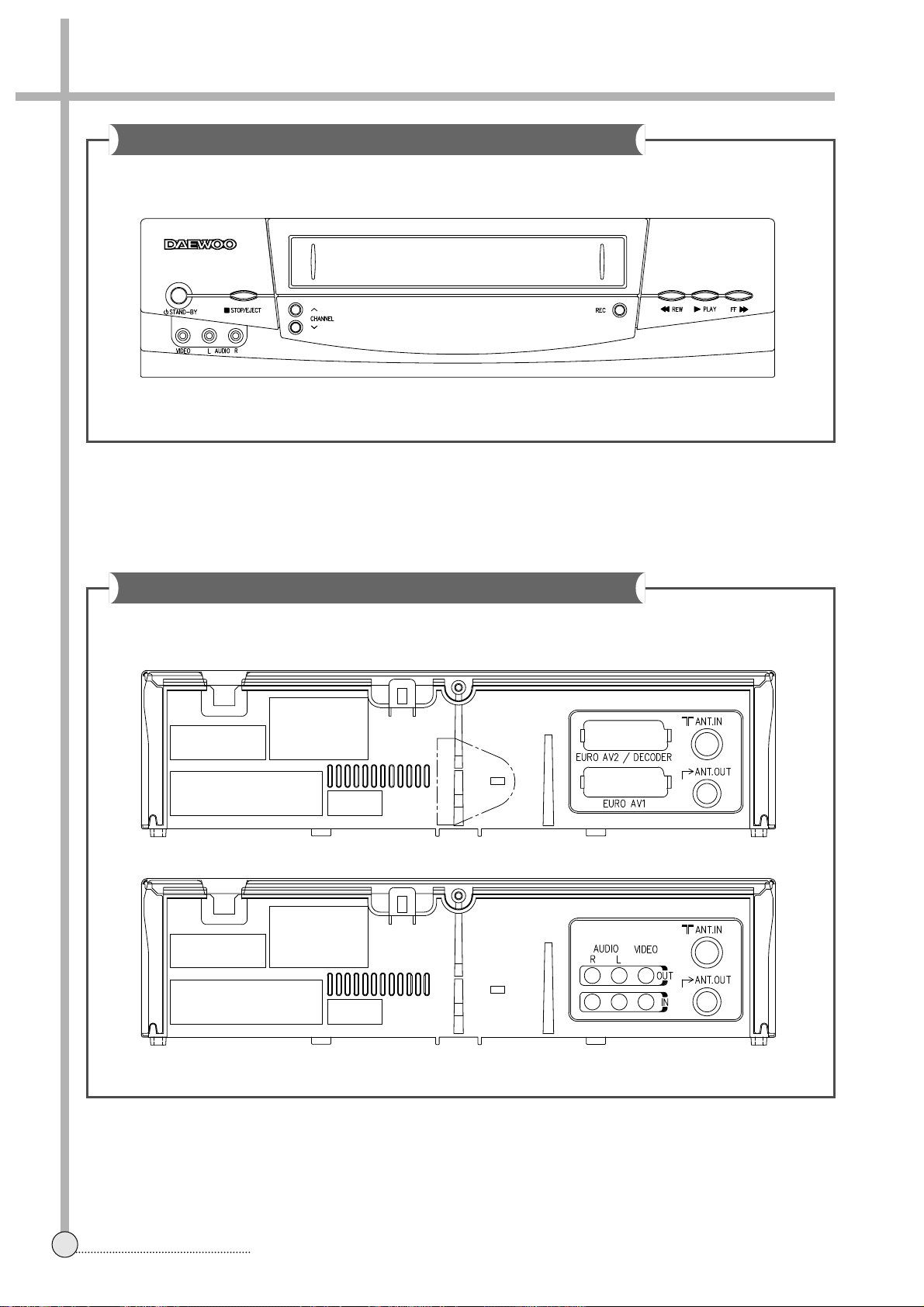
CONTROLS & FUNCTIONS
SECTION 1. CONTROLS AND FUNCTIONS
Front
1 STAND BY
2 STOP/EJECT
3 CHANNEL UP / DOWN SELECTION
4 PLAY BACK
5 REWIND / REVIEW
6 FAST FORWARD / CUE
7 RECORD / OTR (ONE TOUCH RECORDING)
Rear
1 EURO AV2 / DECODER (AV OUT)
2 EURO AV1 (AV IN)
3 ANTENNA INPUT TERMINAL
4 ANTENNA OUTPUT TERMINAL
3
ADJUSTMENTS
SECTION 2. ELECTRICAL ADJUSTMENTS
1. PLAYBA CK PHASE
• CONNECTION METHOD
• ADJUSTMENT PROCEDURE
1) Play back the test tape. (DP-2)
2) Set the oscilloscope to the CHOP mode. Connect CH1 to the SW PULSE (PIN 3 of PT01).
3) Insert P ATH JIG and Press “REC” button on the remote control.
4) Check the position of the V -sync from the rising edge of the SW pulse.
(Standard : 6.5H
±0.5H)
2-1. Servo Circuit Adjustment Method
ADJUSTMENT PARTS
Check
CHECKING POINT
JP037
PT01 PIN 4
Oscilloscope
MODE
Play
TEST TAPE
DP-2
V.OUT
TOP VIEW
PT01
PRE-AMP
CH-2
OSCILLOSCOPE
CH-1
PATH JIG
T
•
M
7
JP037
VIDEO OUT
MEASURING EQUIPMENT
4
ADJUSTMENTS
1. AFT
• AFT CONNECTION METHOD
IF MODULE PCB (TOP VIEW)
2-2. IF Module Circuit Adjustment Methods
ADJUSTMENT PARTS
L101
CHECKING POINT
P102
PIN 7
TEST EQUIPMENTS
Signal Gen.
Oscilloscope
Pow er Supply
INPUT SIGNAL
Refer to the follo wing.
P101P102
GNDCH1
0.5mS/DIV
50mV/DIV(10:1)
OUTPUT
SIGNAL
Modulation Method : 30% AM
fm : 400Hz
fc : 38.9MHz
SIGNAL LEVEL : 80dBµV
GEN.
GND
GND
POWER SUPPLY
+9V +5V
(COMPONENT SIDE)
R191
L101
9 91 1
• ADJUSTMENT PROCEDURE
1)Connect the circuit as above connection diagram.
2) Set the each equipment setting as above description.
3) Adjust L101 to obtain 2.5
±0.15V DC V oltage at check point.
5
ADJUSTMENTS
P101P102
GNDCH1
0.5mS/DIV
0.1V/DIV(10:1)
OUTPUT
SIGNAL
Modulation Method : 30% AM
fm : 1KHz
fc : 38.9MHz
SIGNAL LEVEL : 95dBµV
GEN.
GND
GND
POWER SUPPLY
+9V +5V
(COMPONENT SIDE)
R191
L101
9 91 1
2.2µ/50V
2. RF AGC
• RF AGC CONNECTION METHOD
IF MODULE PCB (TOP VIEW)
ADJUSTMENT PARTS
R191
CHECKING POINT
P101
PIN 7
TEST EQUIPMENTS
Signal Gen.
Oscilloscope
Pow er Supply
INPUT SIGNAL
Refer to the follo wing.
• ADJUSTMENT PROCEDURE
1)Connect the circuit as above connection diagram.
2) Set the each equipment setting as above description.
3) Adjust R191 to obtain 6.0
±0.2V DC V oltage at check point.
6
1. OUTLINE
The part that supply DC VOLTAGE to each circuit change AC input voltage into DC voltage. It is based on
SMPS(switching mode power supply)system which is located on main PCB. SMPS module is composed of the
switching circuit and the transformer of the primary part and the rectifier circuit of the secondary part.
2. NAME AND OPERA TION OF PINS ON SMPS MODULE
1) Primary Part
2) Secondary Part
CIRCUIT
SECTION 3. CIRCUIT OPERATION PRINCIPLES
3-1. Power Circuit
PIN NO
1
2
NAME
AC INPUT
FUNCTION
SUPPLY AC INPUT VOLTAGE
PIN NO
1
2
3
4
5
6
7
8
9
NAME
+38V
(F+4.5V)
(F-GND)
-23V
GND
GND
GND
6V
12.4V
FUNCTION
TURN VOLTAGE OF
TUNER (33V)
F/L DISPLAY FILAMENT
VOLTAGE SUPPLY
F/L DISPLAY FILAMENT
VOLTAGE SUPPLY
F/L DISPLAY DRIVE
VOLTAGE SUPPLY
SECONDARY GND
SECONDARY GND
SECONDARY GND
EVER 5V, ON/OFF 5V
CAP MOT, DRUM MOT (12V)
LOADING MOT (12V)

7
3. GENERAL CIRCUIT OPERA TION
The circuit shown is a highly accurate 38V, 12.5V, 6.0V, -24V, 4.5V, 20W secondary regulated flyback power supply
that will operate from 85V to 265 VAC input voltage.
The input voltage is rectified and filtered by D801 and C1. L801, C801, C804 reduce conducted emissin current.
C806, L801, C805 reduce common mode noises. R801 is ESD path resistor.
V oltage feedback is obtained from the transformer (T11) bias winding, which eliminates the need for optocoupler and
secondary-referenced error amplifier. High-Voltage DC is applied to the pr imary-high-voltage DC is applied to the
primary-winding of T11.
The other side of the transformer primary is driven by the integrated high-voltage MOS FET-transistor within the
TOP214 (IC11). The circuit operates at a switching frequency of 100KHz, set by the internal oscillator of the TOP
(IC11). The clamp circuit impelemented by DZ11, D11, C17 and R13 limits the leading-edge voltage spike caused by
transformer leakage inductance to a safe value.
The 38V power secondary winding is rectified by DC1, C25. The 12.5V power secondary winding is rectified and
filtered by D24, C24. The 6.0V power secondary winding is rectified and filtered by D23, L22, C23. The -24V power
secondary winding is rectified and filtered by DC2 and C22. The F(+) and F(-) power secondar y winding is rectified
and filterd by DC3, C21 and C29.
A IC21(KA431) shunt regulator directly senses and accurately regulates the output voltage. The effective output
voltage can be file turned by adjusting the resistor divider formed by R24, R25 and R26. Other output voltages are
possible by adjusting the transformer turns ratio as well as the divider ratio.
The IC21(KA431) regulates the output voltage by controlling optocoupling LED current (and IC11 duty cycle) to
maintain an average voltage of 2.5V at the IC21 input pin.
Divider R24, R25 and R26 determine the actual output voltage. C27, R27 rolls off the high frequency gain of the
KA31 for stable operation.
R23 limits optocoupler LED current and determines high-frequency loop gain. SPFT star t capacitor C26 increases
optocoupler current turn-on to limit the duty cycle and down the r isting output voltage. C26 has minimal effect on the
control loop during normal operation. R22 dicharges soft start capacitor C26 when input power is removed.
The output of the T11 bias winding is rectified and filtered by D12, C11 and R11 to create a typical 12V bias voltage
R12, R13 together with the control pin dynamic impedance and capacitor ESR establish a control loop pole-zero pair.
C13, R12 also determines the auto frequency and filters internal gate drive switching current.
CIRCUIT
8
CIRCUIT
1. LA71511M(QOP 80 PIN) : LUMINANCE-CHROMINANCE AND NORMAL AUDIO SIGNAL PROCESSING IC
1) Applicable to multi system : PAL-GBI, MESECAM, 4.43NTSC, NAP-GBI
2) Built-in NAP circuit to convert NTSC to PAL
3) Normal audio signal processing circuit (self-alignment for record bias)
4) Built-in record and playback FM-EQ function (I
2
C bus control)
5) Y/C separation using built-in comb filter
6) Built-in switching circuit for 3 video/audio inputs
7) Serial control by I
2
C-bus
8) Complete adjustment free
9) Crosstalk reduction by CCD IC for exclusive use (Color comb filter is unnecessary)
2. LA70011(4CH) : PRE-AMP IC
1) AGC circuit is built-in this IC (no record current adjustment is required)
2) Playback envelope detector circuit is built-in this IC for the purpose of auto-tracking
3. LC89977M : CCD DELAY LINE IC
1) Built-in comb filter function for color noise reduction
2) Built-in 1H delay line for luminance signal
3-2. Key Features of Video IC and Its Relatives
1. RECORD PROCESSING
The video input signal selected by the A/V switching IC(KA8119B) among AUX video input, Front video input and IF
video input, is supplied to the 35th pin of A/V 1CHIP IC.
The input video signal is then automatically adjusted to suitable level by the built-in A GC circuit and supplied to SYNC
SEPARATION and FBC(feedback clamp) part respectively.
SYNC signal obtained from the composite video signal by SYN SEP circuit is supplied to the 93rd pin MICOM to
determine the presence of signal and to control the SERVO LOGIC.
In PRE-AMP IC, fir HEAD AMP switching timing on TRICK PLAY and AGC circuit for self-aligning the record bias.
The signal through FBC is then processed in luminance signal processing par t and chrominance signal processing
part independently.
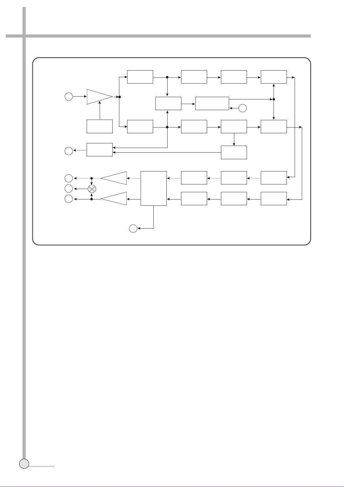
3-3. Record and Playback Processing Circuit
PDC IC 13th PIN
LUMINANCE SIGNAL PROCESSING
CHROMINANCE SIGNAL PROCESSING
MICOM 93rd PIN
PRE-AMP IC 5th PIN
VIDEO
INPUT
35 37VIDEO AGC SYNC SEP
FBC
FIG.1 Record Processing
9
CIRCUIT
1) LUMINANCE SIGNAL PROCESSING (RECORD)
The input signal through FBC is reduced a half(-6dB) of its level and then the pure luminance signal is obtained by
LPF. In YNR(luminance noise reduction) circuit, noise is eliminated using the original signal and the 1H delayed
signal.
The DETAIL ENHANCER enhances the overall high-frequency response, so an object with fine lines (such as a lawn,
hair etc.) can be seen more clearly during PLAYBACK.
The NONLINEAR EMPHASIS and MAIN EMPHASIS can minimize the triangular noise susceptible to frequency
modulation.
The luminance signal is FM-modulated and then is supplied to RECORD EQUALIZER for compensating the high
frequency response related to HEAD characteristic, where its RECORD EQ is determined by the GROUP 4, LSB 1-4
bits of I
2
C serial control.
2) CHROMINANCE SIGNAL PROCESSING (RECORD)
The pure chrominance signal is obtained by BPF1 (fsc : 4.43MHz), which filters the input signal through FBC.
The gain of ACC AMP is controlled by the DC voltage at 13th pin.
The main converter down-converts the chrominance signal with signal carrier of 4.43MHz to the signal with signal
carrier of 627KHz.
The down-converted signal is again filtered by the LPF, so the pure chrominance component is maintained.
Meanwhile, the burst level of the ACC AMP output signal is detected by the burst gate, and it determines the
activation of color killer.
18
40
5 42
25 26
7
400nS
DELAY FILTER
(LC89977M)
PRE-AMP 9th PIN
CLAMP
1H DELAY
FBC 1/2 LPF YNR
REC EQ FM MOD
MAIN
EMPHASIS
DETAIL
ENHANCER
N.L.
EMPHASIS
CLAMP
FIG.2 Luminance Signal Processing (RECORD)
14
13
FBC BPF 1 ACC
AMP
MAIN
CONV
C-LPF KIL PRE-AMP 10th PIN
REC
DET
REC
BGA
FIG.3 Chrominance Signal Processing (RECORD)
10
CIRCUIT
2. PLAYBA CK PR OCESSING
PLAYBACK ENVELOPE signal from the PRE-AMP IC is supplied to the 15th pin of A/V IC for processing the PAL
color, luminance respectively.
The output signal through Y/C MIX after each processing of chrominance and luminance is supplied to the 18th pin
of OSD IC.
1) LUMINANCE SIGNAL PROCESSING (PB)
The PLAYBACK ENVELOPE signal is equalized by the PB-EQ, which flattens the whole frequency characteristic.
And the PB-EQ is determined by the GROUP , MSB 7-8 bits.
Phase compensation part improves the pulse characteristics.
DOUBLE LIMITER restores the high frequency portion, and eliminates the spike noise, and AM components.
The signal through DOUBLE LIMITER is then demodulate, and then the RECORD NONLINEAR EMPHASIS
characteristic is compensated by the DE-EMPHASIS.
Double High Pass Noise Canceller eliminates the high frequency noise against PB signal.
The Picture Control circuit improves the picture sharpness, while its characteristic is deter mined by the GROUP 8,
LSB 1-4 bits.
15
25
542 7 40
26
17 20PB-EQ PHASE COMP
DOUBLE LIMITERSUB-LPF
CLAMP LPF YNR N.L. DE-EM DHP NC
FM DEMOD
PIC CTL Y/C MIX
Y/C MIX
(LC89977M)
CLAMP
FM AGC
PRE-AMP 7th PIN
FIG.5 Luminance Signal Processing (PB)
PB ENVE
PRE-AMP
7th PIN
35
38
Y/C MIX
FBC VIDEO AMP
luminance signal
processing
chrominance signal
processing
OSD IC 18th PIN
FIG.4 Playback Processing
11
CIRCUIT
2) CHROMINANCE SIGNAL PROCESSING (PB)
The down-converted chrominance signal is obtained from PB ENVE signal by LPF first. And then the signal is upconverted to 4.43MHz by the MAIN CONVERTER.
The redundant harmonics is filtered out by the BPF, and then the signal is applied to the CCD IC to reduce the
chrominance crosstalk.
The NTSC PLAYBACK is possible on PAL/SECAM SYSTEM by the NAP circuit, the activation of which is determined
by GROUP 7, MSB 7-8 bits.
The signal is then applied to Color Noise Canceller and mixed together with the luminance signal.
15
501
483
+1352
46 45
13
PRE-AMP
7th PIN
LPF ACC AMP MAIN CONV BPF2 BPF1
2H DELAY
(LC89977M)
Y/C MIXCNCBPFNAP
KIL LPF AMP
FIG.6 Chrominance Signal Processing (PB)

12
1. VIDEO SIGNAL FLOW
The signal from the ANT is amplified for selectivity, to decrease image interference, and increase S/N using the RF
AMP. The RF signal at the MIXER is subtracted from the LOCAL OSC frequency using the upperside band method,
to change it into the IF signal; 38.9MHz. The IF signal converted from the RF signal in the tuner block is amplified by
about 20dB to increase S/N in the pre-amp block. The reason for thesis that the SAW filter has its own insertion loss
of about -18 to -22dB. The SAW filter is a kind of BPF, used to remove the near channel harmonics and make the
desired frequency response. The IF AMP desired of about 60 to 70dB gain for receiver sensitivity and selectivity. The
vision IF AMP consists of three AC-coupled differential amplifier stages; each stage uses a controlled feedback
network called AGC. To maintain the video output signal at a constant level the automatic control voltage is generated
according to the transmission standard. For negative modulation in the PAL standard the peak-sync level is detected.
The AGC detector charges and discharges the AGC capacitor to set the IF gain and the tuner gain. We can also
adjust the tuner AGC voltage take over point. This allows the tuner and the IF SAW filter to be matched to achieve the
optimum IF input signal. The IF amplifier output signal is fed to a frequency detector and to a phase detector. The
frequency detector is operational before lock-in. A DC current is generated which is proportional to the frequency
difference between the input signal and the VCO frequency. The control voltage for the VCO is provided by the phase
detector. The demodulate output signal is fed via an integrated LPF (about 12MHz) to the video amplifier for
suppression of the carrier harmonics.
The VCO operates with a symmetrically-connected reference L-C circuit, running at the double vision carrier
frequency (77.8MHz) to decrease the frequency error. Frequency control is performed by an internal varicap diode.
The voltage used to set the VCO frequency to the actual double vision carrier frequency, is also amplified and
converted to give the AFC output current. The AFC output is fed to the µ-COM to change the LOCAL OSC frequency
and for channel searching. The VCO signal is divided by-two in a travelling wave divider, which generates two
differential output signals with exactly 90 degrees phase difference, independent of frequency. The video signal
passing through the 5.5MHz sound trap is fed to the buffer.
3-4. IF Circuit Operation
PRE-
AMP
MIXER
LOCAL
OSC
TUNER
SAW
FILTER
VIDEO DET
& DE MOD
VCO AFC
SOUND
TRAP
BUFFER
RF
AMP
IF
AMP
VIDEO
OUT
µ-COM
AGC
DET
CIRCUIT
13
CIRCUIT
2. PAL AUDIO FLOW (Tw o carrier)
The FM sound intercarrier signal passing through the 5.5MHz/5.74MHz (DK : 6.5MHz) sound BPF is fed to a limiter
amplifier before it is demodulate. This gives high sensitivity and AM suppression. The limiter amplifier consists of
seven internal AC-coupled stages, minimizing the DC offset. The FM-PLL demodulator consists of an RC-oscillator,
loop filter and phase detector. The oscillator frequency is locked on to the FM intercarrier signal from the limiter
amplifier. As a result of this locking, the RC-oscillator is frequency modulated. The modulating signal voltage is used
to control the oscillator frequency using this technique, the FM-PLL works as a FM demodulator. The audio
signal(AF1:L+R/2, AF2:R+pilot(AM)) passing through the stereo/dual sound processor. Its identification ensures safe
operation by using internal digital PLL technique with extremely small bandwidth, synchronous detection and digital
integration(switching the maximum 2.6s; identification concerning the main functions).
The audio signal(L, R) is amplified and coming out of the stereo/digital sound processor.
3. DIGITAL AUDIO FLO W
The demodulator function includes integrated baseband filters for pulse shaping and unwanted signal rejection,
automatic gain control, a low jitter integrated VCO.
The decoder fucntion performs the descrambling, de-interleaving and reformatting operations required to recover the
original data words.
The data words are processed through a stereo digital filter, digital de-emphasis network, second order noise shaper,
and 256 times over sampling bitstream audio DA C.
The whole device supported by 8.192MHz crystal oscillator, and I
2
C serial data bus for communications with µ-com.
In the output stage out selector can automute the nicam signal to normal audio when the digital data have noise
more than error rate.
BASE BAND
FILTER
&
AGC GAIN
STAGE
PHASE DETECT
&
DATA
SLICERS
NICAM728
DECODER &
DEVICE
CONTROLLER
DIGITAL
FILTER
&
NOISE
SHAPER
BITSTREAM
DAC
OUT S/W
&
BUFFER
DQPSK
OUT L
OUT R
I C DATA X-TAL NORMAL AUDIO
2
DECODERDEMODULATOR
VIDEO BLOCK
VIDEO DET
& DEMOD
SOUND
BPF
LIMITER
AMP
FM PLL-
DEMOD.
AUDIO OUT(L)
AUDIO OUT(R)
AF
AMP
DIGITAL PLL-
DEMOD.
DIGITAL
INTEGRATOR
intercarrier
STEREO(LOW)
DUAL(LOW)

14
CIRCUIT
4. TM BLOCK
The TUNER and MODULATOR which is separated to each module conventionally, is presently united to one block
(TM block)
(a) PLL METHOD AND I
2
C-BUS CONTROL
The RF OUTPUT channel can be varied from 22CH to 69CH by remote control using PLL method and I
2
C-BUS
control.
Moreover, SYSTEM(PAL, MESECAM), SOUND CARRIER FREQUENCY, AND TPSG(TEST PATTERN SIGNAL
GENERATOR) can be changed by remote control as well.
The P/S ratio, white clip, power saving, etc., also can be controlled only by changing a I
2
C-BUS data according to
the designer’s intention.
(b) DIGITAL AFT METHOD
Conventionally, when the frequency deviates, the variation of AFT output from IF circuit was compensated by
feedbacking it to TUNER AFT input.
On the other hand, if AFT, which is currently adopted to these models from IF circuit deviates the window range,
the VT value is changed to maintain the AFT voltage to be within window range by checking AFT(+) and AFT(-) on
MICOM.
VOLTAGE
AFT(+)
3V
WINDOW
2V
FREQ.
AFT(-)
15
CIRCUIT
The circuitry of Normal AUDIO part is similar to that of the conventional Nor mal AUDIO part in case of EE and PB
mode, but in REC mode, due to the internal operation of self-alignment, it shows a lot of differences.
1. EE MODE
LA71511M has 3-input VIDEO/AUDIO switching circuitry internally, and its switching is controlled by the serial data
dispatched from MICOM.
But for the suitable operation to these models, only One input is used. The Normal AUDIO signal from Hi-Fi Audio
part is divided by the resistor, R202 and R203 and then supplied to the 73rd pin of LA71511M. Its level is
automatically controlled by ALC and then the amplified signal through LINE AMP is obtained at the 77th pin.
The signal from C208 is supplied to REC AMP after the divider circuit (R204, R205, R207) and also to the Hi-Fi IC
BH7804K.
The ALC point can be adjusted by R208 and R209, the adjustment of which is closely related to the REC level in
REC mode.
The ALC time can be adjusted by R201 and C201.
2. PB MODE
The PB signal picked up from AUDIO HEAD is firstly processed in the frequency characteristic compensator which is
composed of R220 and C214 (EP : C214+C215) and then supplied to the 7th pin.
The input signal passes through EQ AMP, and LINE AMP, so its output signal is finally obtained from the 77th pin.
The circuitry and its operation of EQ AMP is identical to the conventional EQ AMP.
3. REC MODE
1) AUDIO SWITCHING CIRCUIT
When the AUDIO S/W signal at the 80th pin is “H”, the point at the AUDIO HEAD of the e xternal switching circuit is
opened electrically (EE/PB=GND), so the COIL starts to oscillate.
2) As long as the voltage difference between VCC and the 5th pin is maintained at 2.0~4.3V, the COIL oscillates. In
other words, the COIL maintains to oscillate only if the voltage at the 5th pin is 0.7~3.0V
p-p.
Especially, when the R/P and FE HEAD impedance is at the center, the voltage at the 5th pin should be
maintained at 1.85V
p-p, and, if not, when the HEAD impedance is MAX or MIN, the voltage at the 5th pin is liable
to deviate the ranges of 0.7~3.0V
p-p.
The higher the FE HEAD impedance is or the lower the R/P HEAD impedance is, the higher the voltage at the 5th
pin increases.
The AC signal is put on the DC voltage at the 5th pin, and it shows the internal AUTO BIASing.
The control signal at the 6th pin controls the TR(Q205) to ON/OFF, by which the AUTO BIASing is controlled.
3-5. Normal Audio Signal Processing (LA71511M)
REC : OPEN
EE : GND
A-H
S/W
Q202
Q204
Q203
R/P
HEAD
R214
R216
R218
R217
VCC
R215
80
5
BIAS COIL
5th PIN
External Switching Circuit

16
CIRCUIT
3) The output AUDIO signal at the 1st pin through REC AMP is recorded on HEAD after being mixed with the 70KHz
AC BIAS signal.
At the same time, the output AUDIO signal is supplied to the 3rd pin and then filtered by 60KHz HPF, so only the
70KHz AC BIAS signal is passed.
The pure 70KHz AC BIAS signal is then compared to the voltage of 440mV at the comparator, so the AC BIAS
signal is controlled to maintain at 440mV.
4) The recording current is determined by the 440mV
rms BIAS signal and the resistance between the 1st and the 3rd
pin.
* The method to set the recording current.
BIAS = 440mV
rms ÷the resistance between the 1st and the 3rd pin.
ex) 440mV
rms ÷1.8K OHM = 244µA
where, only the low error, G type resistor should be used here.
As a rule of thumb, the resistance between the 1st and the 3rd pin should range from 1.0 ohm to 2.2K ohm.
5) The conventional AUDIO circuitry uses a peaking COIL to enhance the high frequency region, b ut the LA71511M
uses the resistance of R/P HEAD.
Accordingly, The resistor and the capacitor is used to fit the frequency characteristics.
4. BIAS COIL
For normal operation of AUTO BIAS, the oscillating voltage of R/P HEAD is over 40V
p-p, A/E HEAD is over 20Vp-p,
and the FE HEAD is over 40V
p-p.
Especially, the erasing current of F/E HEAD ranges from 130 to 280mA, and it should be 180mA when the HEAD
impedance is at the center.
1. SPECIAL FEA TURES
BH7804K processes the conventional Hi-Fi audio. and additionally, contains special parts as the below.
(1) As
±2 power source formula is adapted, decrease of coupling capacitor is possible. the REGULATOR circuit is
built in.
(2) Built in I
2
C bus control decoder circuit which has two lines formula, each mode for the inside of IC is set up by
serial data.
(3) Reverse characteristics system during recording and playback are used in both the PNR (Peak Noise
Reduction) processor and FM MODEM. And it can be simultaneous adjustment of carrier frequency and FM
deviation/playback level. And it can be independent adjustment of FM deviation/playback level. (The adjustment
of Lch and Rch is simultaneous.)
(4) Slope control FM switching noise correction circuit is built in.
(5) Auto adjust circuit of VCO and BPF making use of Fsc(4.43MHz) is built in. It is possible to adjust changelessly
without drift by board mounting stress and time.
BA7746FS contains the functions as the below
(1) Built-in VCA for easy adjustment of play back output level.
(2) Total gain 79dB of low noise Pre amp for play bac k mode .
(3) Built-in LPF to regulate input band width of recording amp.
(4) Recording amp has high output current for audio FM recording.
3-6. Hi-Fi Audio Signal Processing (BH7804K)
2. REC MODE
(1) Signal Flow
In this system, the input signal sources are contained with IF, AV1, AV2/C+ and F.AV. each pin number’s decription is
the same as the below.
The input signals, selected by the input switcher , go through the LPF (at 20KHz) and PNR processor. Additionally, the
selected input signals are supplied to the Normal Audio Unit-Pin 31st. The Normal Audio cab be mixed with the L+RStereo mode, or can be selected with L only-Bilingual mode. The PNR processor compresses the audio signal in
order to reduce the audio noise and enlarge the Dynamic Range.
The FM EMPH(FM Emphasis) emphasizes the higher band of signal. It can restrict the FM back-noise, when the
signal is demodulated. the modified audio signal is modulated by the Modulator unit. It is composed of AUDIO
LIM(Limitter), 1.4MHz & 1.8MHz modulator. The Audio limiter cuts the level of signal to avoid the overmodulation, and
then the limitted signal is modulated with two carriers-1.4MHz : Left Ch, 1.8MHz : Right Ch. The modulated two
signals are mixed by the FM MIX unit. The mix ratio of FM L and R can be adjusted with the software-refer to the
service mode. Finally, REC FM signal put out to the Pin 21st. It is supplied to the Hi-Fi preamp.
(2) Auto Adjustment of the VCO, BPF
In this IC, the FM carrier frequency and BPF are adjusted by the synthesized PLL VCO (Phase Locked Loop Voltage
Control) unit. the Auto adjustment is executed at POWER ON, as using the Fsc-4.43MHz. The Fsc is supplied from
the OSC for Color Sub-carrier in the Video unit. If the adjustment completes successfully, IC’s pin 14th is set the
“HIGH” state-5V. Otherwise “LOW” state-0V. The adjustment of VCO, BPF occurs simultaneouslly.
17
CIRCUIT
AUDIO IN
NORMAL AUDIO
L
R
31
8
INPUT
SW
LPF
LPF
PNR
PNR
FM
EMPH
FM
EMPH
LPF
LPF
1.4M
MOD
AUTO
ADJ
FM
MIX
AUDIO
LIM
AUDIO
LIM
REC FM
LPF
REC FM
LPF
1.8M
MOD
Fsc
21
REC FM OUT
INPUT
CH
L
R
IF
2
1
A V1
44
43
A V2/C+
41
40
F.A V
34
33
3. PB MODE
(1) Signal Flow
FM signal input to the Pin 13rd is amplified, and ditributed to the two BPFs-1.4MHz and 1.8MHz. The band passed
FM signals are supplied to the De-Modulator unit. First, the FM LIM confines the FM to the limitted level, and then the
signals are demodulated. The converted audio signals are compensated by the SW NOISE COMPEN. The signals
are passed by the LPF, and de-emphasized by the FM DE-EMPH in order to restrict the FM back-noise. The PNR
processor expands the signals and reduces the audio noise.
The two Line AMPs amplifiy the audio level, and supply to the Audio Out Pin 30th, 29th. The Mod out Pin 27th is and
mixed audio output port for the RF-modulator. The Output SW is available to select the audio output of Left+Right
(Stereo), Left only, Right only and Normal Audio. The Pin 26th is the input port for Normal audio.
(2) Noise Compensation and Hi-Fi Detect
In the Hi-Fi audio system, the noise trouble occurs, when the FM signal is defective. The defection of FM signal is
due to the Drop Out which is scratched on the surface of tape, and the audio SW noise. If the D.O. DET detects the
Drop Out of FM signal, it requires the HOLD PULSE GEN to generate the hold pulse, and then compensate the
noise. And the HOLD PULSE GEN generates the regular pulse by the Audio SW pulses, then send the control signal
to the SW NOISE COMPEN which compensates the noise.
The ENVE/HiFi discreminates the Hi-Fi audio from the Normal audio. If the envelope of FM Hi-Fi exists, “High”-5Vcontrol signal is out to the Pin 14th. Otherwise Control voltage is 0.
18
CIRCUIT
FM PB IN
13
Hi-Fi DET
14
AUDIO OUT(L)
MOD OUT
30
AUDIO OUT(R)
29
26
8
AMP
LPF
LPF
FM
LIM
DEMOD
D.O.
DET
HOLD
PULSE GEN
SW NOISE
COMPEN.
PNR
OUTPUT
SW
LPF
FM
DE-EMPH
FM
DE-EMPH
FM
LIM
DEMOD
FM
DET
SW NOISE
COMPEN.
FM
ALC
ENVE/
HiFi
A SW
PULSE
PNR
27
AMP
AMP
NORMAL AUDIO
LPF
19
CIRCUIT
ANT IN
1 5
3
3 1
8 30
32
VCR
TUNER
RF MOD
IF BLOCK
DECODER
IN OUT
TV CTL
OUT IN
TV
IN OUT
OUT IN
C+(L)
30
A B C D
LA7152 LA71511M
KA8119B
30
H
H
L
L
AV3
CTL
AV4
CTL
5
38
29 5 4
F
E
F.AV IN
*CTL
AV1
AV2
AV3
AV4
1. KA8119B : Special Functions & Features
(1) Internal Audio/Video Switch for C+. (2-input, 1-output)
(2) Internal Video Selector. (4-input, 1-output)
(3) Internal Video 6dB Amp
(4) Distinguished Supply Voltage. (Audio : 9V, Video : 5V)
2. LA7152 : 3 input, 1 output Video Switcher
3. BLOCK DIAGRAM
3-7. Video/Audio Switching Circuit
Selection T able For K8118B
Selection T able For LA7152
SEL
A
B
C
D
A V3 CTL
L
L
L
H
A V2 CTL
L
L
H
-
A V1 CTL
H
L
L
-
Remarks
Video
Selector
Only
SEL AV3 CTL AV2 CTL AV1 CTL Remarks
E H H H Only Case 12 & 13 in C+ SW Mode
F All cases are selected except for E
20
CIRCUIT
4. SWITCHING OPERA TION
In this switching system, Video signals are selected by two A/V SW ICs (KA8119B & LA7152), Audio signals are
separately selectd by Hi-Fi IC itself which was controlled by the I
2
C bus. - W3D1, W3D2 mean the serial data bits for
the selection. -Refer below the table.
KA8119B contains the C+ SWs for Audio and Video signals. So Video and Audio signals are controlled by AV3 and
AV4 at the same time.
The item “Video Sel” means the input pin number of AV one chip IC(LA71511M). At the case 15, 16 Video input shall
be selected with Pin 32 (C+ discrambled signal).
If the power’s off at the state selected with F.AV, the SW mode is Case 16, 17 (For only VCR mode).
(1) CANAL plus mode.
Audio Sel
Tuner
A V1
A V2 or C+ decoder
F.A V
W3D1
L
H
L
H
W3D2
L
L
H
H
Remarks
MODE
POWER
OFF
PLAY
EE
TV/
VCR
-
-
TV
VCR
TV
VCR
TUNER
/A V
/F .AV
TUNER
AV
-
-
TUNER
AV
F.AV
TUNER
AV
F.AV
REC
-
-
-
-
NO
YES
-
-
-
-
-
C+
MEM
-
-
-
-
-
NO
YES
-
-
-
-
-
C+
NO
YES
NO
YES
NO
YES
-
NO
YES
NO
YES
NO
YES
NO
YES
NO
YES
NO
YES
NO
YES
-
-
TV
CTL
L
H
L
H
L
H
H
L
H
L
H
L
L
L
H
L
H
H
H
H
H
H
H
A V4
CTL
H
L
H
L
H
L
H
H
L
H
L
H
H
H
H
H
L
H
H
H
H
H
H
A V3
CTL
L
L
L
L
L
L
L
L
L
L
L
H
H
L
L
L
L
H
H
L
L
L
L
A V2
CTL
L
L
L
L
L
L
L
L
L
L
L
H
L
L
L
H
H
H
L
L
L
H
H
A V1
CTL
H
H
L
L
H
H
H
H
H
H
H
H
H
L
L
L
L
H
H
L
L
L
L
VIDEO
SEL
PIN30
PIN30
PIN30
PIN30
PIN30
PIN30
PIN30
PIN30
PIN30
PIN30
PIN30
PIN30
PIN30
PIN30
PIN32
PIN30
PIN30
PIN30
PIN30
PIN30
PIN32
PIN30
PIN30
AUDIO
W3D1
L
L
H
H
L
L
L
L
L
L
L
L
L
H
L
H
H
L
L
H
L
H
H
SEL
W3D2
L
L
L
L
L
L
L
L
L
L
L
L
H
L
H
H
H
L
H
L
H
H
H
REMARKS
Case 1
Case 2
Case 3
Case 4
Case 5
Case 6
Case 7
Case 8
Case 9
Case 10
Case 11
Case 12
Case 13
Case 14
Case 15
Case 16
Case 17
Case 18
Case 19
Case 20
Case 21
Case 22
Case 23

21
CIRCUIT
- Case 1
TV set : Watching & receiving the normal CH.
VCR set : Power off, Input source is turner. TV set signal comes out to the decoder.
- Case 2
TV set : Watching the C+ CH which is received by itself .
VCR set : Power off, Input source is tuner, Discramble the C+ and supply it to the TV set.
- Case 3
TV set : Watching & receiving the normal CH.
VCR set : Power off, Input source is AV. TV set signal comes out to the decoder.
- Case 4
TV set : Watching the C+ CH received on itself.
VCR set : Power off, Input source is AV. Discramble the C+ and supply it to the TV set.
- Case 5
TV set : Watching & receiving the normal CH.
VCR set : Play mode. forced TV mode. TV set signal comes out to the decoder .
- Case 6
TV set : Watching the C+ CH received on itself.
VCR set : Play mode, forced TV mode. Discramble the C+ and supply it to the TV set.
- Case 7
TV set : Watching the picture which is played on VCR set.
VCR set : Play, auto VCR mode, TV set signal comes out to the decoder.
- Case 8
TV set : Watching & receiving the normal CH.
VCR set : EE, TV mode. Input source is tuner. TV set signal comes out to the decoder.
- Case 9
TV set : Watching the C+ CH received on itself.
VCR set : EE, TV mode. Input source is tuner. Discramble the C+ and supply it to the TV set.
- Case 10
TV set : Watching & receiving the normal CH.
VCR set : TV mode. No C+ Ch memory. Recording another normal CH received on the VCR set.
TV set signal comes out to the decoder.
- Case 11
TV set : Watching the C+ CH received on itself.
VCR set : TV mode. No C+ CH memory. Recording another normal CH received on the VCR set.
Discramble the C+ and supply it to the TV set.
- Case 12
TV set : Watching & receiving the normal CH.
VCR set : TV mode. C+ CH memory . Recording another normal CH received on the VCR set.
VCR tuner signal comes out to the decoder because of C+ channel memory.
- Case 13
TV set : Watching & receiving the normal CH.
VCR set : TV mode. C+ CH memory . Recording C+ CH received on the VCR set.
VCR tuner signal is discrambled and supplied to the REC path.
In this case, the C+ received on TV cannot be discrambled.

22
CIRCUIT
- Case 14
TV set : Watching & receiving the normal CH.
VCR set : EE, TV mode. Input source is AV. TV set signal comes out to the decoder.
- Case 15
TV set : Watching the C+ CH received on itself.
VCR set : TV mode. Input source is AV. Discramble the C+ and supply it to the TV set.
If a user press the REC button, the VCR set record the Discrambled TV signal.
- Case 16
TV set : Watching & receiving the normal CH.
VCR set : EE, TV mode. Input source is F.AV. TV set signal comes out to the decoder.
If a user press the REC button, the VCR set record the F.AV signal.
- Case 17
TV set : Watching the C+ CH received on itself
VCR set : EE, TV mode. Input source is F.AV. Discramble the C+ and supply it to the TV set.
Although a user press the REC button, the VCR set record the F.AV signal.
- Case 18
TV set : Watching the normal CH received on VCR set.
VCR set : EE, VCR mode, Input source is tuner. Tuner signal comes out to the decoder.
If a user press the REC button, the VCR set record the tuner signal.
- Case 19
TV set : Watching the C+ CH received on VCR set.
VCR set : EE, VCR mode. Input source is decoder . Tuner signal is descrambled and supplied to the REC path.
- Case 20
TV set : Watching the VCR set’s AV signal (TV signal).
VCR set : EE, VCR mode. Input source is AV. AV signal comes out to the decoder.
If a user press the REC button, the VCR set record the AV signal.
- Case 21
TV set : Watching the C+ CH received on itself. (VCR set’s A V signal).
VCR set : EE, VCR mode. Input source is AV. Discramble the C+ and supply it to the TV set.
- Case 22, 23
TV set : Watching the VCR set’s F.AV signal.
VCR set : EE, VCR mode. Input source is F.AV. TV set signal comes out to the decoder.
If a user press the REC button, the VCR set record the F.AV signal.
23
CIRCUIT
(2) Three input One output mode.
(3) Tw o input One output mode.
MODE
POWER
OFF
PLAY
EE/REC
TV/VCR
-
-
-
TV
VCR
TV
VCR
TV
VCR
TV
VCR
TV
VCR
TUNER
/A V1/AV2
/F .AV
TV
AV1
AV2
-
-
TV
AV1
AV2
F.AV
C+
H
L
H
L
H
L
-
-
-
-
-
-
TV
CTL
L
H
L
H
L
H
L
H
L
H
L
L
L
H
L
H
A V4
CTL
L
L
L
L
L
L
H
H
H
H
H
H
H
H
H
H
A V3
CTL
L
L
L
L
H
H
L
L
L
L
L
L
H
H
L
L
A V2
CTL
L
L
L
L
-
L
L
L
L
L
L
-
-
H
H
A V1
CTL
H
H
L
L
-
H
H
H
H
L
L
-
-
L
L
VIDEO
SEL
PIN30
PIN30
PIN30
PIN30
PIN30
PIN30
PIN30
PIN30
PIN30
PIN30
PIN30
PIN30
PIN30
PIN30
PIN32
PIN30
AUDIO
W3D1
H
H
L
L
L
L
H
H
H
H
L
L
L
L
H
H
SEL
W3D2
L
L
L
L
H
H
L
L
L
L
L
L
H
H
H
H
REMARKS
CH SEARCH
CH SEARCH
MODE
POWER
OFF
PLAY
EE/REC
TV/VCR
-
-
TV
VCR
TV
VCR
TV
VCR
TV
VCR
TUNER
/A V1/AV2
/F .AV
TUNER
AV1
-
-
TV
AV1
F.AV
C+
H
L
H
L
-
-
-
-
-
TV
CTL
L
H
L
H
L
H
L
H
L
H
L
H
A V4
CTL
L
L
L
L
H
H
H
H
H
H
H
H
A V3
CTL
L
L
L
L
L
L
L
L
L
L
L
L
A V2
CTL
L
L
L
L
L
L
L
L
L
L
H
H
A V1
CTL
H
H
L
L
H
H
H
H
L
L
L
L
VIDEO
SEL
PIN30
PIN30
PIN30
PIN30
PIN30
PIN30
PIN30
PIN30
PIN30
PIN30
PIN30
PIN30
AUDIO
W3D1
H
H
L
L
H
H
H
H
L
L
H
H
SEL
W3D2
L
L
L
L
L
L
L
L
L
L
H
H
REMARKS
CH SEARCH
CH SEARCH
INFORMATION
•SAFETY CHECK AFTER SER VICING
Examine the area surrounding the repaired location for damage or deterioration. Observe that screws, parts and wires have
been returned to original positions. Afterwards, perform the following tests and confirm the specified values in order to verify
compliance with safety standards.
1. Insulation resistance test
1. Confirm the specified insulation resistance or greater between power cord plug prongs and externally exposed parts of
the set (RF terminals, antenna terminals, video and audio input and output terminals, microphone jacks, earphone jacks,
etc.). See table below.
2. Dielectric strength test
1. Confirm specified dielectric strength or greater between power cord plug prongs and e xposed accessib le parts of the set
1. (RF terminals, antenna terminals, video and audio input and output terminals, microphone jacks, earphone jacks, etc.).
See table below.
3. Clearance distance
1. When replacing primary circuit components, confirm specified 1. 1.
clearance distance (d), (d') between soldered terminals, and
between terminals and surrounding metallic parts. See table below.
T able 1: Rating for selected areas
*Class
IImodel only.
Note: This table is unofficial and for reference only. Be sure to confirm the precise values for your particular
country and locality .
4. Leakage current test
1.Confirm specified or lower leakage current between B (earth ground, power cord plug prongs) and externally exposed 1.
1.accessible.parts (RF terminals, antenna ter minals, video and audio
input and output terminals, microphone jacks, earphone jacks etc.)
1. Measuring Method: (Pow er ON)
1. Insert load Z between B (earth ground, power cord plug prongs)
and exposed accessible parts. Use and AC voltmeter to measure
across both terminals of load Z.
1. See figure and following tab le .
T able 2: Leaka ge current ratings f or selected areas
Note : This table unofficial and for reference only. Be sure to confirm the precise values for your particular
country and locality.
AC Line Voltage
100V
110 to 130V
*110 to 130V
200 to 240V
Region
Japan
USA & Canada
Europe
Australia
Insulation Resistance
≥ 1MΩ/500V DC
_
≥
4MΩ/500V DC
Dielectric Strength
1kV AC 1 minute
900V AC 1 minute
3kV AC 1 minute
Clearance Distance (d), (d’)
≥ 3 mm
≥ 3.2 mm
≥
3mm (d)
≥
6mm (d’)
(a : Power cord)
Chassis
d
d
'
a
Primary circuit terminals
Fig.1
Fig.2
Exposed
accessible
part
Earth Ground
power cord plug prongs
AC voltmeter
(high impedance)
Z
B
AC Line Voltage
100V
110 to 130V
110 to 130V
200 to 240V
Region
Japan
USA & Canada
Europe
Australia
Load Z Leakage Current (i)
i ≤ 1mA rms
i ≤ 0.5mA rms
i≤0.7mA peak
i
≤
2mA dc
i ≤ 0.7mA peak
i ≤ 2mA dc
Earth Ground (B) to:
Exposed accessible parts
Exposed accessible parts
Antenna earth terminals
Other terminals
1KΩ
1.5kµF
KΩ
1.
2KΩ
50KΩ
FLOW CHART
SECTION 4. TROUBLESHOOTING FLOW CHART
When changing the parts which are broken first, remove the power plug from the socket and then discharge the
voltage across the terminals of C807 (use an external 1KΩ(2W) resistance).
When check the primary circuit, Use the oscilloscope isolated proper ly (Use the isolated transformer) and connect
GND to the primary GND, however it is not necessary to isolate the oscilloscope when check the secondary circuit.
A. CHECKING THE PRIMARY CIRCUIT.
4-1. Power Circuit
No output Voltage.
Prepare the oscilloscope
connected the isolated
transformer
Check F801 Fuse.
Is 5.7 voltage applied to
IC11 control pin
Check the secondary circuit
Is voltage applied to D801?
Is voltage applied to the
terminals of C807?
Is varation between 5.7V
and 4.8V at IC11 control pin
Check L801, L802
Check R803, D801
NO
NO
NO
NO
Check T11 : 3~6 pin,
L12 and IC11
YES
YES
YES
YES
YES
YES
24
FLOW CHART
Check each output voltage
END
Check the CN21
Check the diode of NO
output stages
Check transformer of NO
output stages
NO
Check the COIL, C of NO
output stages
YES
YES
YES
YES
B. CHECKING THE SECONDARY CIRCUIT
25
26
FLOW CHART
A. TROUBLESHOOTING OF RF RECEIVING CIRCUIT
Is Video Signal at Video Out point,
P101 Pin No. 4 of IF Module?
Check the A/V Switching and Video
Circuit.
YES
Is Audio Signal at Audio Out point,
P102 Pin No.2/No.4 of IF Module?
YES
NO
NO
YES
YES
YES
YES
Is +5V supplied to BB point,
Pin No. 1 of TM Block?
Check the Power Supply Circuit.
NO
Is +9V supplied to IF 9V point,
P101 Pin No. 3 of IF Module?
Check Q179, Q180 and Power
Supply Circuit.
NO
Check Q177, Q178 and Power
Supply Circuit.
NO
Check Q181, EVER 33V and then
PWM from µ-COM.
NO
YES
Is RF AGC adjusted well?
YES
Change the IF Module and then
TM Block.
Correct RF AGC adjustment.
NO
YES
Is AFT adjusted well?
Correct AFT adjustment.
NO
Check the transistors from Q171 to
Q176 and µ-COM ports, VL(H),
VH(H) and UHF(H)
NO
Is +9V supplied to VL, VH or U
band point, Pin No. 15, 16 or 17 or
TM Block?
Is tunning voltage changed
when changing channels?
Is +5V supplied to IF 5V point,
P102 Pin No. 5 of IF Module?
4-2. PIF Circuit Troubleshooting
27
FLOW CHART
B. TROUBLESHOOTING OF RF MODULATOR OUT
Is Video Signal at Video In point,
Pin No. 6 of TM Block?
Check the A/V Switching, Video and
Audio Circuit.
NO
Is Audio Signal at Audio In point,
Pin No. 2 of TM Block?
NO
YES
YES
YES
YES
YES
YES
Are RF OUT System and RF Out
channel selected well by menu key.
Select the RIGHT System and
channel by menu key.
NO
Is system Select Option Diode
applied well according to Option
Table?
Correct the Option.
NO
Is +5V supplied to MB point,
Pin No. 4 of TM Block?
Check on/off 5V and Power Supply
Circuit.
NO
Is +30V supplied to TU(MD) point,
Pin No. 7 of TM Block?
Check D171 and Power Supply
Circuit.
NO
YES
Is Serial Clock supplied to SCL
points, Pin No. 5 of TM
Block?
YES
Change the TM Block.
Check the µ-COM port, SCL.
NO
Check the µ-COM port, SDA.
NO
Is Serial Data supplied to
SDA points, Pin No. 3 of TM
Block?
 Loading...