


DAEWOO DV-F462N, DV-F262N, DV-F482N, DV-F282N, DV-F542N Service Manual
...
Service Manual
MODEL : DV-F462N/262N
DV-F482N/282N
DV-F542N/342N
DV-F442N/242N/X
NEW PCB Model of
DV-F46N/26N
DV-F48N/28N
DV-F54N/34N
DV-F44N/24N/X
PLAY
REW FF
FF
POWER EJECT
STOP
REC / OTR
CH/TRACK
DAEWOO ELECTRONICS CO., LTD.

SPECIFICATIONS
Power Source: |
120V 60Hz |
|
Power Consumption: |
Approx. 17 watts |
|
Temperature: |
41°F to 104°F |
|
Television System: |
USA-525 lines, 60 fields NTSC standard |
|
Video Signal System: |
NTSC type color signal |
|
Video Recording System: |
Luminance: FM azimuth recording color phase shift and |
|
|
converted subcarrier direct recording |
|
Scanning System: |
Rotary, slant azimuth, helical scanning system, 2 head, |
|
|
4 head double Azimuth |
|
Tuner: |
181 Channel Freq. Synthesized |
|
|
VHF : 2-13 |
|
|
UHF : 14-69 |
|
|
CATV: 14-36(A)-(W), 37-59(AA)-(WW), 60-85(AAA)-(ZZZ), |
|
|
86-94(86)-(94), 95-99(A-5)-(A-1), 100-125(100)-(125), |
|
|
01(5A) |
|
Audio Track: |
1 Track |
|
Tape Speed: |
SP: 1-5/16"/sec. |
|
|
LP: 21/32"/sec. |
|
|
EP: 7/16"/sec. |
|
Visual Search Speed: |
SP-3 X Normal Speed |
|
|
LP-5 X Normal Speed |
|
|
EP-5 X Normal Speed |
|
Record/Playback Time: |
Max. 8 Hours T-160 at EP |
|
FF/REW Time: |
Less than 5.0 min. with T-120 tape |
|
Heads: |
Video: |
2 rotary heads (VR-4250), 4 head double azimuth (VR-4450) |
|
Audio/Control: |
1 stationary head |
|
Erase: |
1 full track erase |
Modulator: |
Signal Strength: |
66 dBµ/75 ohm |
RF Channel Output: |
Channel 3 or 4, switchable |
|
Input Level: |
Video: 1.0Vp-p 75 ohm (RCA) |
|
|
Audio: -8dB/50K ohm (RCA) |
|
Output level: |
Video: 1.0Vpp 75 ohm (RCA) |
|
|
Audio: –6dB/1K ohm (RCA) |
|
Weight: |
9.1 Lbs |
|
Dimensions: |
14.2(W) X 12.3(D) X 3.5(H) Inches |
|
1
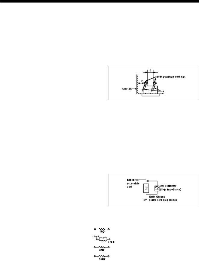
• Safety Check after Servicing
Examine the area surrounding the repaired location for damage or deterioration. Observe that screws, parts and wires have been returned to original positions. Afterwards, perform the following tests and confirm the specified values in order to verify compliance with safety standards.
1.Insulation resistance test
Confirm the specified insulation resistance or greater between power cord plug prongs and externally exposed parts of the set (RF terminals, antenna terminals, video and audio input and output terminals, microphone jacks, earphone jacks, etc.). See table below.
2.Dielectric strength tes
Confirm specified dielectric strength or greater between power cord plug prongs and exposed accessible parts of the set (RF terminals, antenna terminals, video and audio input and output terminals, microphone jacks, earphone jacks, etc.) See table below.
3.Clearance distance
When replacing primary circuit components, confirm specified clearance distance (d), (d') between soldered terminals, and between terminals and surrounding metalic parts. See table below.
Table 1: Rating for selected areas |
|
Fig. 1 |
|
||
|
|
|
|
|
|
|
AC Line Voltage |
Region |
Insulation |
Dielectric |
Clearance |
|
Resistance |
Strength |
Distance (d), (d') |
||
|
|
|
|||
|
100V |
Japan |
≥ 1 MΩ /500 V DC |
1kV 1 minute |
≥ 3 mm |
|
110 to 130V |
USA & |
– – – |
900V 1 minute |
≥ 3.2mm |
|
Canada |
||||
|
|
|
|
|
|
|
|
South |
|
|
≥ 6 mm (d) |
|
* 100 to 250 V |
≥ 10 MΩ /500 V DC |
4 kV 1 minute |
≥ 8 mm (d') |
|
|
America |
||||
|
|
|
|
(a: Power cord) |
|
|
|
|
|
|
|
Note: This table is unofficial and for reference only. Be sure to confirm the precise values for your particular country and locality.
4.Leakage current test
Confirm specified or lower leakage current between B (earth ground, power cord plug prongs) and externally exposed accessible parts (RF terminals, antenna terminals, video and audio input and output terminals, microphone jacks, earphone jacks, etc.)
Measuring Method: (Power ON)
Insert load Z between B (earth ground, power cord plug prongs) and exposed accessible parts. Use and AC voltmeter to measure across both terminals of load Z. See figure and following table.
Table 2: Leakage current ratings for selected areas |
|
|
Fig. 2 |
|
||
|
|
|
|
|||
|
|
|
|
|
|
|
AC Line Voltage |
Region |
|
Load Z |
Leakage Current (i) |
Earth Ground |
|
|
(B) to: |
|||||
|
|
|
|
|
|
|
100V |
Japan |
|
|
|
¡ ≤ 1m A rms |
Exposed accessible |
|
|
|
parts |
|||
|
|
|
|
|
|
|
110 to 130 V |
USA & |
|
|
|
¡ ≤ 0.5 m A rms |
Exposed accessible |
|
Canada |
|
|
|
|
parts |
|
|
|
|
|
¡ ≤ 0.7 m A peak |
Antenna earth |
100 to 130 V |
South |
|
|
|
¡ ≤ 2 m A dc |
terminals |
200 to 250 V |
America |
|
|
|
¡ ≤ 0.7 m A peak |
Other terminals |
|
|
|
|
|
¡ ≤ 2 m A dc |
|
|
|
|
|
|
|
|
Note: This is table unofficial and for reference only. Be sure to confirm the precise values for your particular country and locality.

TABLE OF CONTENTS
SPECIFICATIONS ................................................................................................................................................................. |
1 |
CONTROLS AND FUNCTIONS ..................................................................................................................................... |
4 |
ELECTRICAL ADJUSTMENTS |
|
ADJUSTMENT PROCEDURES ........................................................................................................................................................... |
7 |
MAJOR COMPONENTS COCATION GUIDE ..................................................................................................................................... |
8 |
BLOCK DIAGRAM |
|
VIDEO.................................................................................................................................................................................................... |
9 |
2HD PRE-AMP.................................................................................................................................................................................... |
10 |
4HD PRE-AMP.................................................................................................................................................................................... |
11 |
AUDIO ................................................................................................................................................................................................. |
12 |
SYSCON/SERVO/TIMER & LOGIC ................................................................................................................................................... |
13 |
OSD..................................................................................................................................................................................................... |
14 |
PIF & INPUT ........................................................................................................................................................................................ |
15 |
POWER ............................................................................................................................................................................................... |
16 |
PRINTED CIRCUIT BOARDS |
|
MAIN PCB........................................................................................................................................................................................... |
17 |
LOGIC PCB .................................................................................................................................................................................. |
18~19 |
HEAD AMP PCB................................................................................................................................................................................. |
20 |
SCHEMATIC DIAGRAMS |
|
4HD VIDEO SCHEMATIC................................................................................................................................................................... |
21 |
2HD VIDEO SCHEMATIC................................................................................................................................................................... |
22 |
4HD PREAMP SCHEMATIC .............................................................................................................................................................. |
23 |
2HD PREAMP SCHEMATIC .............................................................................................................................................................. |
24 |
AUDIO SCHEMATIC........................................................................................................................................................................... |
25 |
LOGIC SCHEMATIC .................................................................................................................................................................... |
26~27 |
SYSCON/SERVO/TIMER SCHEMATIC ............................................................................................................................................ |
28 |
OSD SCHEMATIC .............................................................................................................................................................................. |
29 |
PIF & INPUT SELECTOR SCHEMATIC............................................................................................................................................. |
30 |
POWER SUPPLY SCHEMATIC (I)..................................................................................................................................................... |
31 |
POWER SUPPLY SCHEMATIC (II) .................................................................................................................................................... |
32 |
CONNECTION DIAGRAM.................................................................................................................................................................. |
33 |
WAVEFORM & VOLTAGE CHART |
|
LUMA/CHROMA WAVEFORMS................................................................................................................................................. |
34~35 |
AUDIO WAVEFORMS ........................................................................................................................................................................ |
36 |
SERVO WAVEFORMS ....................................................................................................................................................................... |
37 |
SERVO/SYSCON/TIMER VOLTAGE CHARTS .......................................................................................................................... |
38~40 |
AUDIO VOLTAGE CHARTS ............................................................................................................................................................... |
40 |
POWER VOLTAGE CHARTS ............................................................................................................................................................. |
40 |
OSD VOLTAGE CHARTS................................................................................................................................................................... |
41 |
VIDEO (LUMA/CHROMA) VOLTAGE CHARTS ................................................................................................................................ |
42 |
PRE AMP VOLTAGE CHARTS .......................................................................................................................................................... |
43 |
PIF & INPUTS SELECT VOLTAGE CHART....................................................................................................................................... |
44 |
EXPLODED VIEW AND PARTS LIST.................................................................................................................. |
45~51 |
MACHANICAL EXPLODED VIEW ....................................................................................................................... |
52~53 |
DISASSEMBLY............................................................................................................................................................... |
54~58 |
ELECTRICAL REPLACEMENT PARTS LIST ................................................................................................. |
59~66 |
2

KEY TO ABBREVIATIONS
A |
AC |
: Alternating Current |
|
FSC |
: Frequency Sub Carrier |
|
REEL S |
: Reel Sensor |
|
A/C |
: Audio/Control |
|
FWD |
: Forward |
|
REF |
: Reference |
|
ACC |
: Automatic Color Control |
G |
GND |
: Ground |
|
REW |
: Rewind |
|
A.E. |
: Audio/Erase |
H |
H.P.F |
: High Pass Filter |
|
REG |
: Regulated, Regulator |
|
AFC |
: Automatic Frequency Control |
|
H.A.SW |
: Head Amp Switch |
|
RF |
: Radio Frequency |
|
AFT |
: Automatic Fine Tuning |
|
H. SYNC |
: Horizontal Sync. |
S |
SEL |
: Select, Selector |
|
AGC |
: Automatic Gain Control |
I |
IF |
: Intermediate Frequency |
|
SIF |
: Sound Intermediate Frequency |
|
AMP |
: Amplifier |
|
|
|
|
SP |
: Standard Play |
|
ANT |
: Antenna |
L |
LED |
: Light Emitting Diode |
|
STB |
: Serial Strobe |
|
APC |
: Automatic Phase Control |
|
LIMIT |
: Limiter |
|
SVC |
: Service |
B |
BGP |
: Burst Gate Pulse |
|
LM |
: Loading Motor |
|
SW |
: Switch |
|
B.P.F |
: Band Pass Filter |
|
LOAD |
: Loading |
|
SYNC SEP |
: Sync Separator, Separation |
|
B/W |
: Black and White |
|
LP |
: Long Play |
T |
TR |
: Transistor |
C |
CAP |
: Capstan |
|
L.P.F |
: Low Pass Filter |
|
TRACK |
: Tracking |
|
CAR |
: Carrier |
|
LUMI |
: Luminance |
|
TRICK |
: Trick Playback |
|
CCD |
: Charged Coupled Device |
M |
MM |
: Monostable Multivibrator |
|
TP |
: Test Point |
|
CH |
: Channel |
|
MOD |
: Modulator, Modulation |
U |
UNREG |
: Unregulated |
|
CLK |
: Clock |
|
MS SW |
: Mech State Switch |
V |
VCO |
: Voltage Controlled Oscillator |
|
COMP |
: Comparator |
N |
NC |
: Non Connection |
|
VIF |
: Video Intermediate Frequency |
|
C ROTARY |
: Color rotary |
O |
OSC |
: Oscillator |
|
VFD |
: Vacuum Fluorescent Display |
|
C SYNC |
: Composite Sync |
|
OSD |
: On-Screen Display |
|
VR |
: Variable Resistor |
|
CONV |
: Converter |
P |
PB |
: Playback |
|
V-SYNC |
: Vertical-Synchronization |
|
CTL |
: Control |
|
PB-C |
: Playback-Chrominance |
|
VXO |
: Voltage Controlled Oscillator |
|
CYL |
: Cylinder |
|
PB-Y |
: Playback-Luminance |
Y |
Y/C |
: Luminance/Chrominance |
D |
DC |
: Direct Current |
|
PCB |
: Printed Circuit Board |
|
|
|
|
DC ENVE |
: DC Envelope Voltage |
|
PG |
: Pulse Generalor |
|
|
|
|
DET |
: Detector |
|
PIF |
: Picture Intermediate Frequency |
|
|
|
|
DEV |
: Deviation |
|
PLL |
: Phase Lock Loop |
|
|
|
|
DOC |
: Drop-Out Compensation |
|
PS |
: Phase Shift |
|
|
|
E |
EE |
: Electric to Electric |
|
PWM |
: Pulse Width Modulation |
|
|
|
|
EP |
: Extended Long Play |
Q |
Q.V. |
: Quasi Vertical Sync |
|
|
|
|
EQ |
: Equalizer |
R |
REC |
: Recording |
|
|
|
F |
FG |
: Frequency Generator |
|
REC-C |
: Recording-Chrominance |
|
|
|
|
FM |
: Frequency Modulation |
|
REC-Y |
: Recording-Luminance |
|
|
|
PREVENTIVE CHECKS AND SERVICE INTERVALS
|
|
|
|
TIME (OPERATING HOURS) |
|
|
|
|
|
|
|
|
|
|
|
PARTS NAME |
|
1000 |
2000 |
|
3000 |
4000 |
5000 |
|
|
|
|
|
|
|
|
DRUM ASS'Y |
|
ƒN |
O |
|
ƒN |
O |
ƒN |
|
|
|
|
|
|
|
|
CAPSTAN MOTOR |
|
|
O |
|
|
O |
|
|
|
|
|
|
|
|
|
L/C BRKT ASS'Y |
|
|
O |
|
|
O |
|
|
|
|
|
|
|
|
|
REEL BELT |
|
|
O |
|
|
O |
|
|
|
|
|
|
|
|
|
IDLER PLATE ASS'Y |
|
ƒN |
|
|
O |
|
|
|
|
|
|
|
|
|
|
REEL TABLE |
|
|
|
|
O |
|
|
|
|
|
|
|
|
|
|
T-SUB BRAKE ASS'Y |
|
O |
|
|
O |
|
|
|
|
|
|
|
|
|
|
BAND BRAKE ASS'Y |
|
O |
|
|
O |
|
|
|
|
|
|
|
|
|
|
S-MAIN BRAKE ASS'Y |
|
O |
|
|
O |
|
|
|
|
|
|
|
|
|
|
T-MAIN BRAKE ASS'Y |
|
O |
|
|
O |
|
|
|
|
|
|
|
|
|
|
PINCH ROLLER ASS'Y |
|
ƒN |
|
O |
ƒN |
|
|
|
|
|
|
|
|
|
|
AC HEAD ASS'Y |
|
|
|
|
O |
|
|
|
|
|
|
|
|
|
|
FE HEAD |
|
|
|
|
|
|
O |
|
|
|
|
|
|
|
|
REEL GEAR ASS'Y |
|
|
ƒN |
|
|
O |
|
|
|
|
|
|
|
|
|
: CHECK, CLEAN |
O : REPLACE |
|
|
|
|
|
|
3
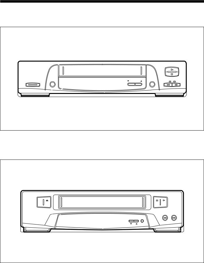
CONTROLS AND FUNCTIONS
FRONT |
|
|
|
|
|
DV-F462/262N |
|
|
|
|
|
|
|
|
|
PLAY |
|
POWER |
EJECT |
|
REC/OTR |
STOP |
|
CH./TRACKING |
FF |
||||
|
|
REW |
|||
DV-F482/282N |
|
|
|
|
POWER |
EJECT |
STOP |
PLAY |
|
|
CH |
REC |
REW |
FF |
|
|
|
||
|
4 |
|
|
|
FRONT |
|
|
|
DV-F542/342N |
|
|
|
|
POWER |
|
|
|
|
PAUSE |
STOP |
CH |
CH |
/ STILL |
|
|
EJECT |
PLAY |
|
|
|
|
|
|
|
REC/OTR |
|
DV-F442/242N/X |
|
|
|
|
|
PLAY |
|
REW |
FF |
POWER |
EJECT |
STOP |
|
|
|
|
REC / OTR |
|
|
CH/TRACK |
|
|
5 |
|
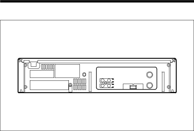
REAR |
|
|
ANT.IN |
VIDEO AUDIO |
|
IN |
RF OUT |
OUT |
CH.4 |
CH.3 |
6

ELECTRICAL ADJUSTMENTS
ADJUSTMENT PROCEDURES
Read and perform these adjustments when repairing the circuits or replacing electrical parts or PCB assemblies.
CAUTION: Inferior silicon grease can damage transistors. When replacing transistors, use only specified silicon grease.
Remove all old silicon before applying new silicon.
1. PG SHIFTER
CONDITIONS
MODE-PLAYBACK
Input Signal-Alignment Tape (DN-1).
INSTRUCTIONS
1.Connect CH-1 on the oscilloscope to pin ¤Ø of PT01 and CH-2 to Video output JACK.
2.Adjust R595 so that the waveform of the oscilloscope measures 6.5±0.5(H) at both leading and trailing edges. (Refer to Fig. 5-1-A, B)
CH-2
6.5H |
CH-1 |
Fig 5-1-A
2. COMB FILTER
CONDITIONS
MODE-STOP
Input Signal-NTSC Multiburst (VIDEO IN JACK)
INSTRUCTIONS
1.Connect the video signal generator to VIDEO IN JACK.
2.Connect CH-1 on the oscilloscope to TJ303 and CH-2 to TJ304.
3.Trigger the scope with CH1.
4.Adjust R494 until the 3.58MHz component of multiburst signal becomes minimum. (Refer to Fig. 5-2)
Fig 5-2
3. AUDIO BIAS
CONDITIONS
MODE-RECORD (SP MODE)
Input Signal-Audio Signal : No Signal
INSTRUCTION
Connect the AC voltmeter as shown, then adjust the voltage to 3.0±0.1mVrms with R292 (Refer to fig. 3-6).
CH-2 |
A/C Head. |
|
|
|
|
CH-1 |
|
AC Voltmeter |
|
TP2 |
TP1 |
|
|
|
6.5H |
(GND) |
|
|
|
|
Fig 5-1-B |
|
Fig 5-3 |
|
|
7
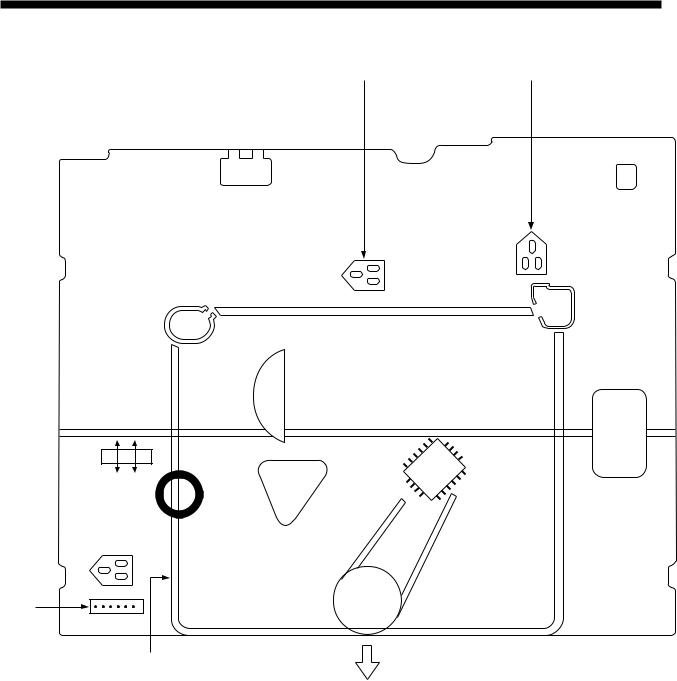
MAJOR COMPONENTS LOCATION GUIDE
VR292 |
VR595 |
A/V JACK
SUPPLY
TJ303
POWER
TJ304
VR494 
PT01
DECK ASSEMBLY |
FRONT |
8
BLOCK DIAGRAMS
VIDEO
9

2HD PRE-AMP
10

4HD PRE-AMP
11

AUDIO
12

SYSCON/SERVO/TIMER & LOGIC
13

OSD
14

PIF & INPUT
15

POWER
16

PRINTED CIRCUIT BOARDS
MAIN PCB
17

LOGIC PCB
DV-F462N/262N
DV-F482N/282N
18
DV-F542N/342N
DV-F442N/242N/X
19
 Loading...