


DV-F562
DAEWOO DV-F562, DV-F362, DV-F542, DV-F342, DV-F442 Service Manual
...
DAEWOO ELECTRONICS CO., LTD.
Service Manual
MODEL : DV-F562/F362 Series
DV-F542/F342 Series
DV-F442/F242 Series
DV-F462/F262 Series
DV-F482/F282 Series
DV-F402/F202 Series
APR. NO : S003GBA PRINTED DATE NOV. 1996
SERVICE MANUAL FM Series
• Safety Check after Servicing
Examine the area surrounding the repaired location for damage or deterioration. Observe that screws, parts and wires
have been returned to original positions. Afterwards, perform the following tests and confirm the specified values in order
to verify compliance with safety standards.
1. Insulation resistance test
Confirm the specified insulation resistance between power cord plug prongs and externally exposed parts of the set
(RF terminals, antenna terminals, video and audio input and output terminals, microphone jacks, earphone jacks, etc.) is
greater than values given in table 1 below.
2. Dielectric strength test
Confirm specified dielectric strength between power cord plug prongs and exposed accessible parts of the set (RF
terminals, antenna terminals, video and audio input and output terminals, microphone jacks, earphone jacks, etc.) is
greater than values given in table 1 below.
3. Clearance distance
When replacing primary circuit components, confirm
specified clearance distance (d), (d') between soldered
terminals, and between terminals and surrounding
metallic parts. See table below.
Table 1: Rating for selected areas
* Class
II model only.
Note: This table is unofficial and for reference only. Be sure to confirm the precise values for your particular country and
locality.
4. Leakage current test
Confirm specified or lower leakage current between B (earth ground, power cord plug prongs) and externally exposed
accessible parts (RF terminals, antenna terminals, video and audio input and output terminals, microphone jacks,
earphone jacks, etc.)
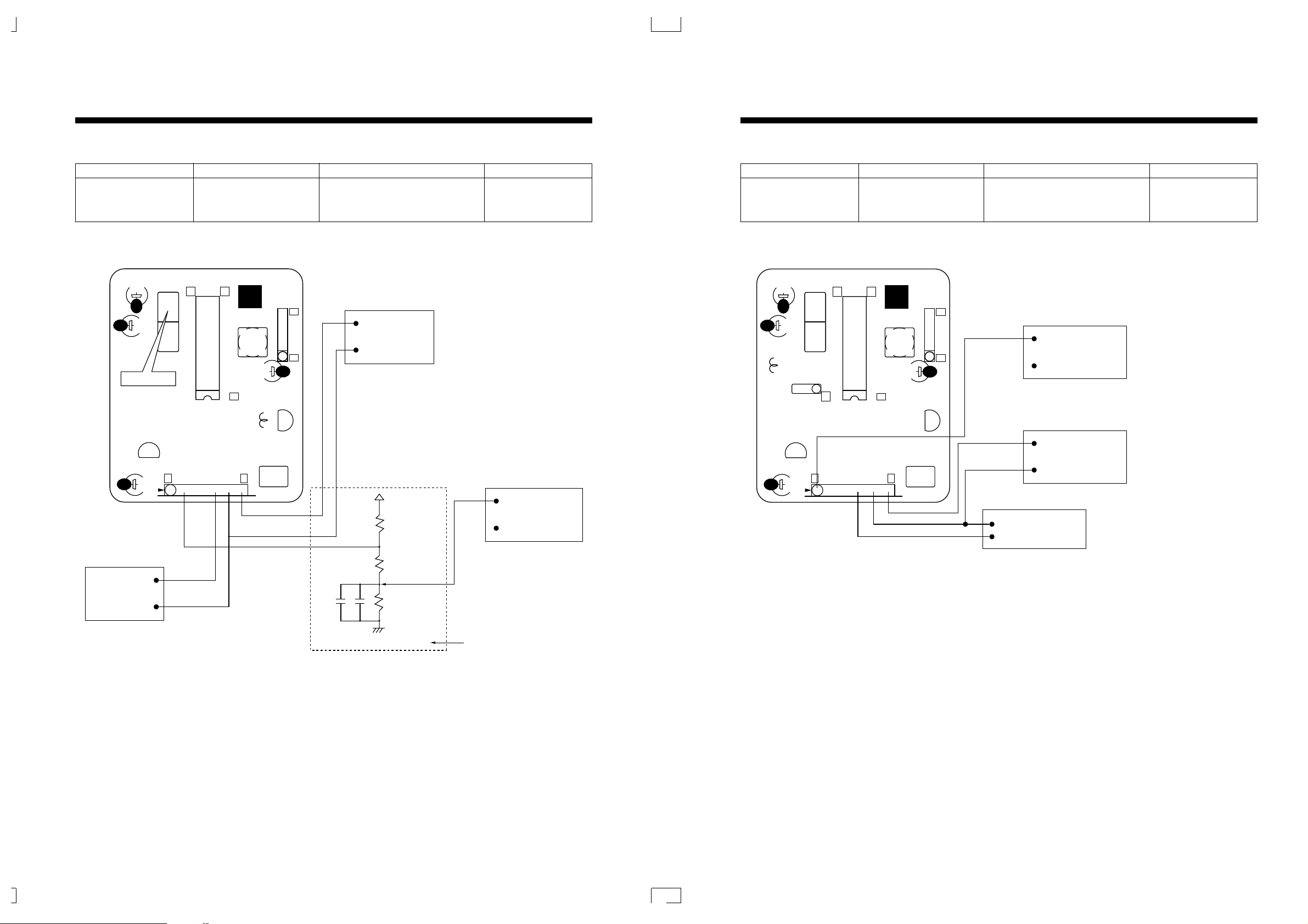
Measuring Method: (Power ON)
Insert load Z between B (earth ground, power cord plug
prongs) and exposed accesible parts. Use an AC
voltmeter to measure across both terminals of load Z.
See figure2 and following table.
Table 2: Leakage current ratings for selected areas
Note: This table is unofficial and for reference only. Be sure to confirm the precise values for your particular country and
locality.
Fig. 2
AC Line Voltage Region
Insulation Dielectric Clearance
Resistance Strength Distance (d), (d')
100V Japan ≥ 1 MΩ/500 V DC 1kV AC 1 minute ≥ 3 mm
110 to 130V
USA &
– – –
900V AC 1 minute ≥ 3.2mm
Canada
* 110 to 130 V Europe ≥ 4 MΩ/500 V DC 3 kV AC 1 minute ≥ 3 mm (d)
200 to 240 V Australia ≥ 6 mm (d')
(a: Power cord)
AC Line Voltage Region
Earth Ground
Load Z Leakage Current (
i
)
(B) to:
100V Japan
i≤ 1 m A rms Exposed accessible
parts
110 to 130 V USA & i≤0.5 m A rms Exposed accessible
parts
i≤ 0.7 m A peak Antenna earth
110 to 130 V Europe i≤ 2 m A dc terminals
200 to 240 V Australia i≤ 0.7 m A peak
Other terminals
i≤2 m A dc
Fig. 1
1k
1.5k
1.5kµF
2k
50k
d
Primary circuit termimals
Chassis
d'
a
Z
Exposed
accessible
part
AC Voltmter
(high impedance)
Earth Ground
power cord plug prongsB
SPECIFICA TIONS
SYSTEM
Video signal PAL standard colour
PAL/SECAM
channel memory 40 positions
UHF output signal 30-39 CH (adjustable)
73±3dBuV
VIDEO
Input: Video Line in 1.0Vp-p
75 ohms unbalanced, sync.
negative
Output: Video line out 75 ohms unbalanced, sync.
negative
Signal to noise ratio More than 43dB (SP)
Horizontal resolution 230 lines
AUDIO
Input: Audio Line in Impedance: more than
50Kohm
–8 dBm, unbalanced
Output: Audio line out Impedance: less than 1Kohm
–6 dBm, unbalanced
Frequency response 100 Hz-8KHz
Signal to noise ratio More than 38 dB
Audio Distortion Less than 3% (SP)
TAPE TRANSPOR T
Tape width 12.65mm (1/2")
Tape speed 23.39mm/sec
Maximum recording time 180 min, with E-180 tape (EP)
FF. REW time Approx 4 min (E-180)
GENERAL
Power requirements AC 230V 50Hz
Power consumption 17W
DIMENSIONS
Set size (WxHxD) 360x90x312 mm
Carton size (WxHxD) 445x180x412 mm
Weight (gross) 5.4Kg
Channel coverage
SYSTEM
PAL,SECAM-B/G
PAL-I/I PAL,SECAM-B/G
PAL,SECAM-B/G,D/K WIDE BAND
PAL-I PAL-B/H
HYPER BAND
VHF Ch 2~12 VHF Ch 2~12 VHF LOW
UHF Ch 21~69 UHF Ch 21~69 Ch 1A~5
Channel CATV Ch X,Y,Z CATV Ch X,Y,Z UHF Ch 21~69 VHF High
SI~S41 SI~S20 Ch 5A~N11
UHF Ch 21~69
IN/OUTPUT JACK TYPE
Model EUROPE
Asia
South Africa
Australia
JACK
SCART Type
RCA JACK
TYPE (PHONE JACK)
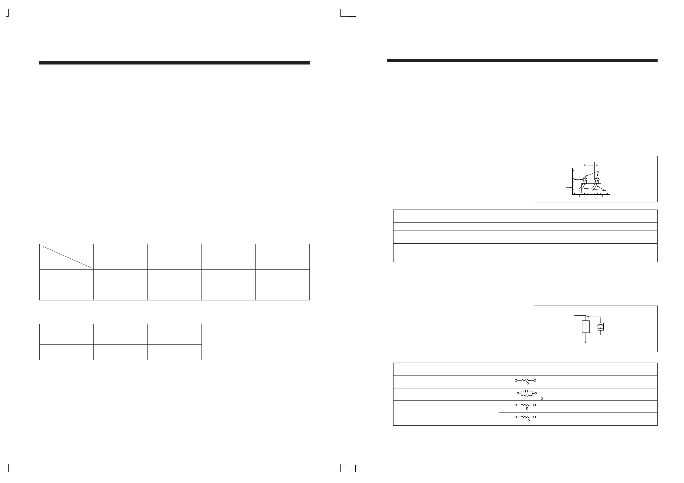
SECTION 1. CONTROLS AND FUNCTIONS
2
TABLE OF CONTENTS
SECTION 1. CONTROLS AND FUNCTIONS..........................................................................................................2
SECTION 2. ELECTRICAL ADJUSTMENTS
2-1. SERVO CIRCUIT ADJUSTMENT METHOD.....................................................................................................................5
2-2. VIDEO CIRCUIT ADJUSTMENT METHOD.......................................................................................................................6
2-3. AUDIO CIRCUIT ADJUSTMENT METHOD.................................................................................................................... 12
2-4. IF MODULE CIRCUIT ADJUSTMENT METHOD ...........................................................................................................13
SECTION 3. TROUBLE SHOOTING FLOW CHART
3-1. POWER CIRCUIT.............................................................................................................................................................17
3-2. LOGIC CIRCUIT...............................................................................................................................................................19
3-3. SERVO-SYSCON CIRCUIT............................................................................................................................................. 21
3-4. AUDIO CIRCUIRT............................................................................................................................................................26
3-5. VIDEO CIRCUIT ...............................................................................................................................................................28
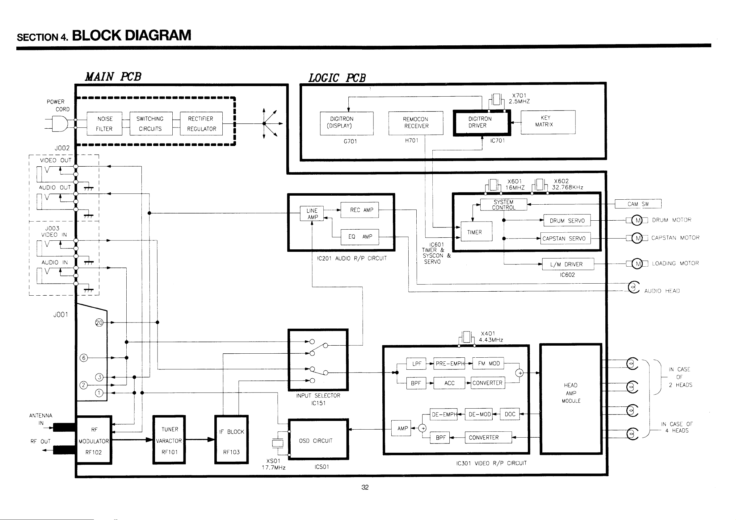
SECTION 4. BLOCK DIAGRAM..................................................................................................................................32
SECTION 5. CIRCUIT DIAGRAM
5-1. CONNECTION DIAGRAM CIRCUIT ...............................................................................................................................33
5-2. POWER CIRCUIT (230V ONLY)......................................................................................................................................34
5-3. POWER CIRCUIT (WIDE RANGE)...................................................................................................................................36
5-4. SERVO-LOGIC CIRCUIT.................................................................................................................................................37
5-5. LOGIC CIRCUIT (F542/F342 Series)...............................................................................................................................38
5-6. LOGIC CIRCUIT (F442/F242, F462/F262, F402(1)/F202(1) Series)...............................................................................39
5-7. LOGIC CIRCUIT (F562/F362 Series)...............................................................................................................................40
5-8. LOGIC CIRCUIT (F402(2)/F202(2) Series)....................................................................................................................... 41
5-9. A/V SW CIRCUIT I............................................................................................................................................................42
5-10. A/V SW CIRCUIT II.........................................................................................................................................................43
5-11. PIF CIRCUIT................................................................................................................................................................... 44
5-12. HEAD-AMP CIRCUIT.....................................................................................................................................................45
5-13. VIDEO CIRCUIT .............................................................................................................................................................47
5-14. OSP CIRCUIT.................................................................................................................................................................48
5-15. COLOR CONVERTER ...................................................................................................................................................49
5-16. LINEAR AUDIO CIRCUIT...............................................................................................................................................50
5-17. IF MODULE CIRCUIT ...................................................................................................................................................51
5-18. VPS CIRCUIT................................................................................................................................................................52
5-19. VPS/PDC CIRCUIT (AUTO-SET)..................................................................................................................................53
5-20. REMOCON CIRCUIT (VR-F3BC).................................................................................................................................54
5-21. REMOCON CIRCUIT (VR-F2BC).................................................................................................................................55
5-22. REMOCON CIRCUIT (VR-F2BT)..................................................................................................................................56
SECTION 6. VOLTAGE CHAR T....................................................................................................................................57
SECTION 7. COMPONENTS LOCA TION GUIDE ON PCB BOTTOM VIEW........................................65
SECTION 8. DISASSEMBLY.......................................................................................................................................... 71
SECTION 9. ELECTRICAL P AR TS LIST..................................................................................................................75
SECTION 10. OPTION T ABLE............................................................................................................................... .......92
1
POWER
EJECT
REC /OTR
CH/TRACK
REW FF
PLAY
STOP
PAUSE
/ STILL
STOP
PLAY
POWER
CH CH
EJECT
REC/OTR
POWER
EJECT REC/OTR
REW FF
PLAY
STOP
CH./TRACKING
FRONT
DV-F542/F342 Series
DV-F462/F262 Series
DV-F442/F242 Series
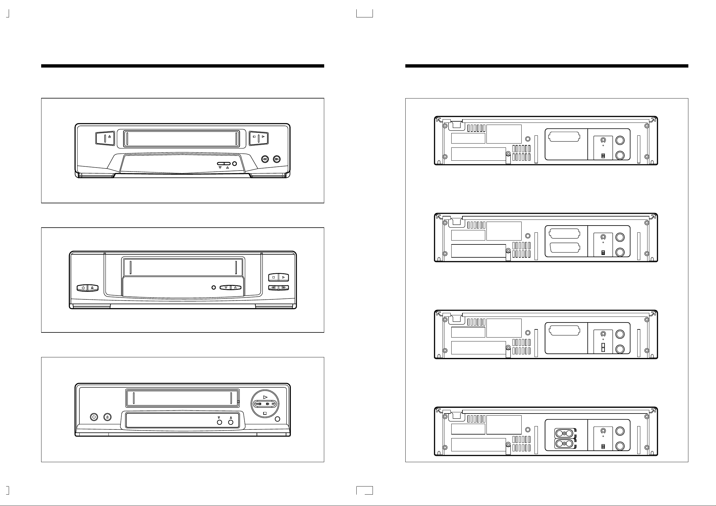
4
RF OUT
ANT. IN
EURO-AV
OFF
CH.H CH.L
TEST
ON
RF OUT
ANT. IN
EURO A/V
OFF
CH.H CH.L
TEST
ON
RF OUT
ANT. IN
EURO-AV
CH.H CH.L
TEST
RF OUT
ANT. IN
OFF
CH.H CH.L
TEST
ON
CANAL
K
G
ON
OFF
OUT
IN
VIDEO AUDIO
REAR
EUROPEAN MODEL (NORMAL)
EUROPEAN MODEL (Canal+)
EASTERN EUROPEAN MODEL
AUSTRALIA/ASIA./SOUTH AFRICA/MIDDLE EAST
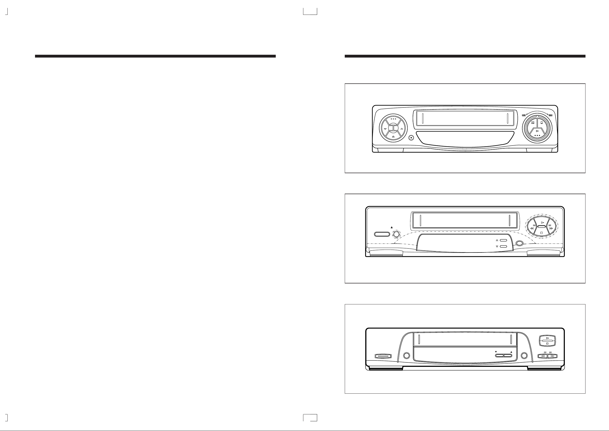
3
POWER EJECT
REC/OTR CH./TRK.
STOP PLAY
REW FF
FFREW
PLAYSTOP
RECCH
EJECT
POWER
POWER
CHANNEL
STOP
PLAY
REW
FF
REC/OTR
EJECT
FRONT
DV-F482/F282 Series
DV-F562/F362 Series
DV-F402/F202 Series
6
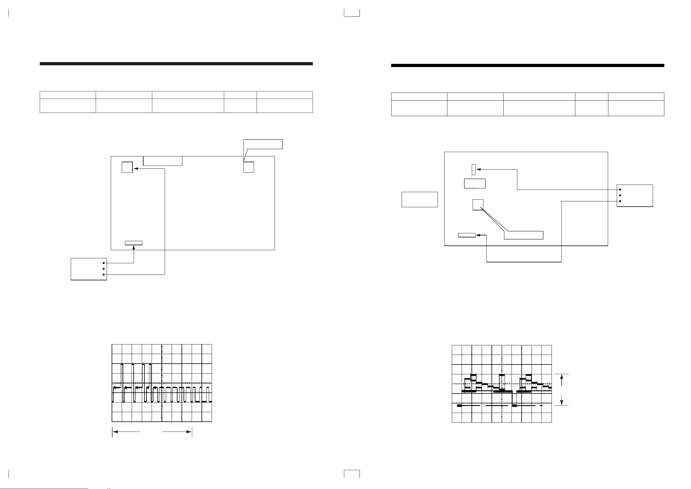
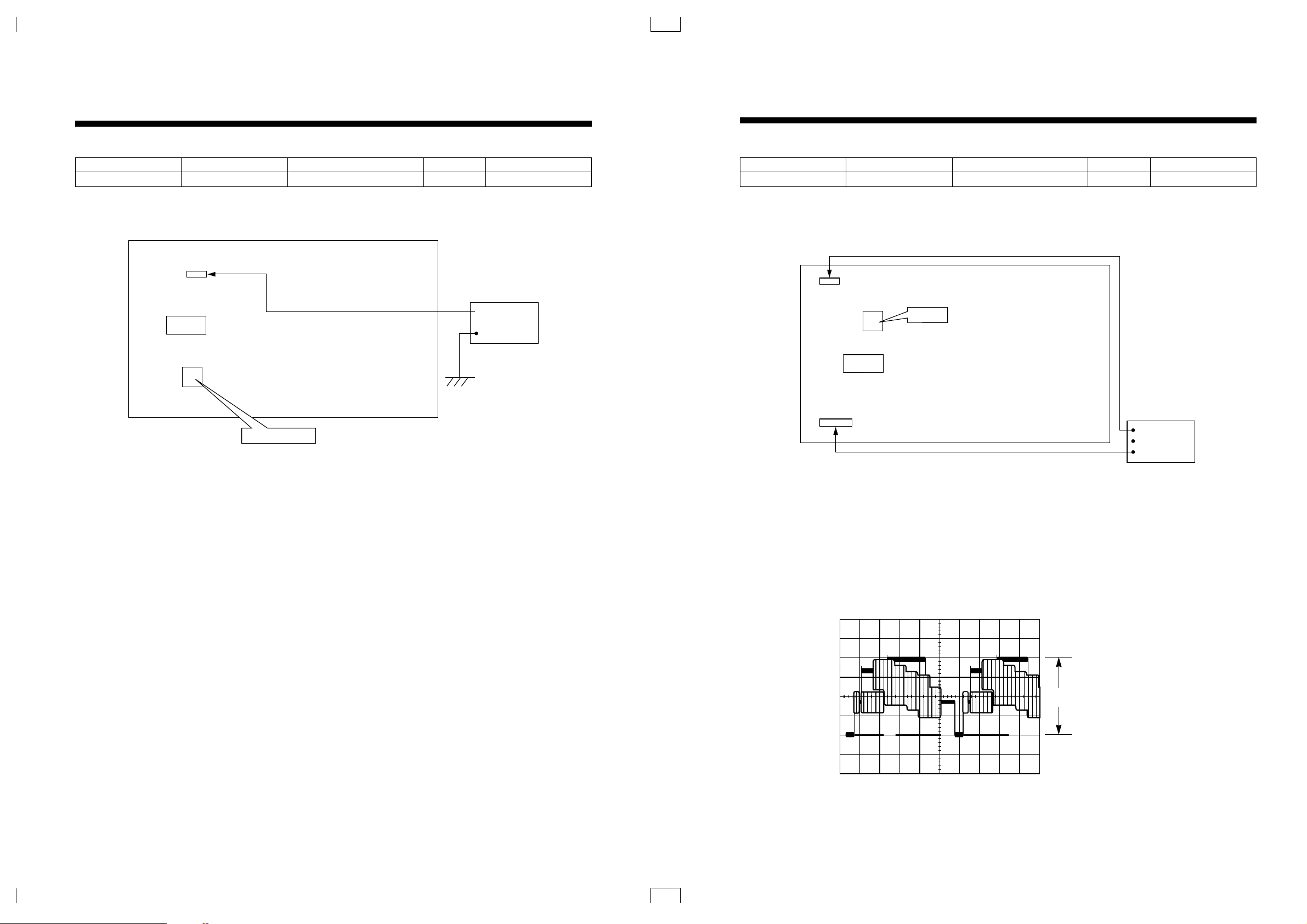
2-2. VIDEO CIRCUIT ADJUSTMENT MENT METHOD
1. EE LEVEL
• Connection Method
• Adjustment Procedure
1) Set the TV/LINE to LINE mode.
2) Supply the Color bar signal with 100% white to the VIDEO IN TERMINAL.
3) Set the VCR to the STOP mode.
4) Connect the oscilloscope to TJ395 and trigger the scope externally with the composite synchronous signal from TJ313
5) Adjust R395 to obtain 0.5 ± 0.02Vp-p between the SYNC TIP and 100% white level.
Adj. Location Checking Point Measuring Equipment Mode Test Tape
R395
TJ313
Signal Gen, Oscilloscope –
Color Bar With 100%
TJ395 White
TJ395
R395
TJ313
TOP VIEW
IC301
0.5
+
_ 0.02Vpp
CH-1
OSCILLOSCOPE
CH-2
SIGNAL
GENERATOR
0.5±0.02Vp-p
TJ 395
Horizontal: 10µs/div
vertical : 0.1v/div
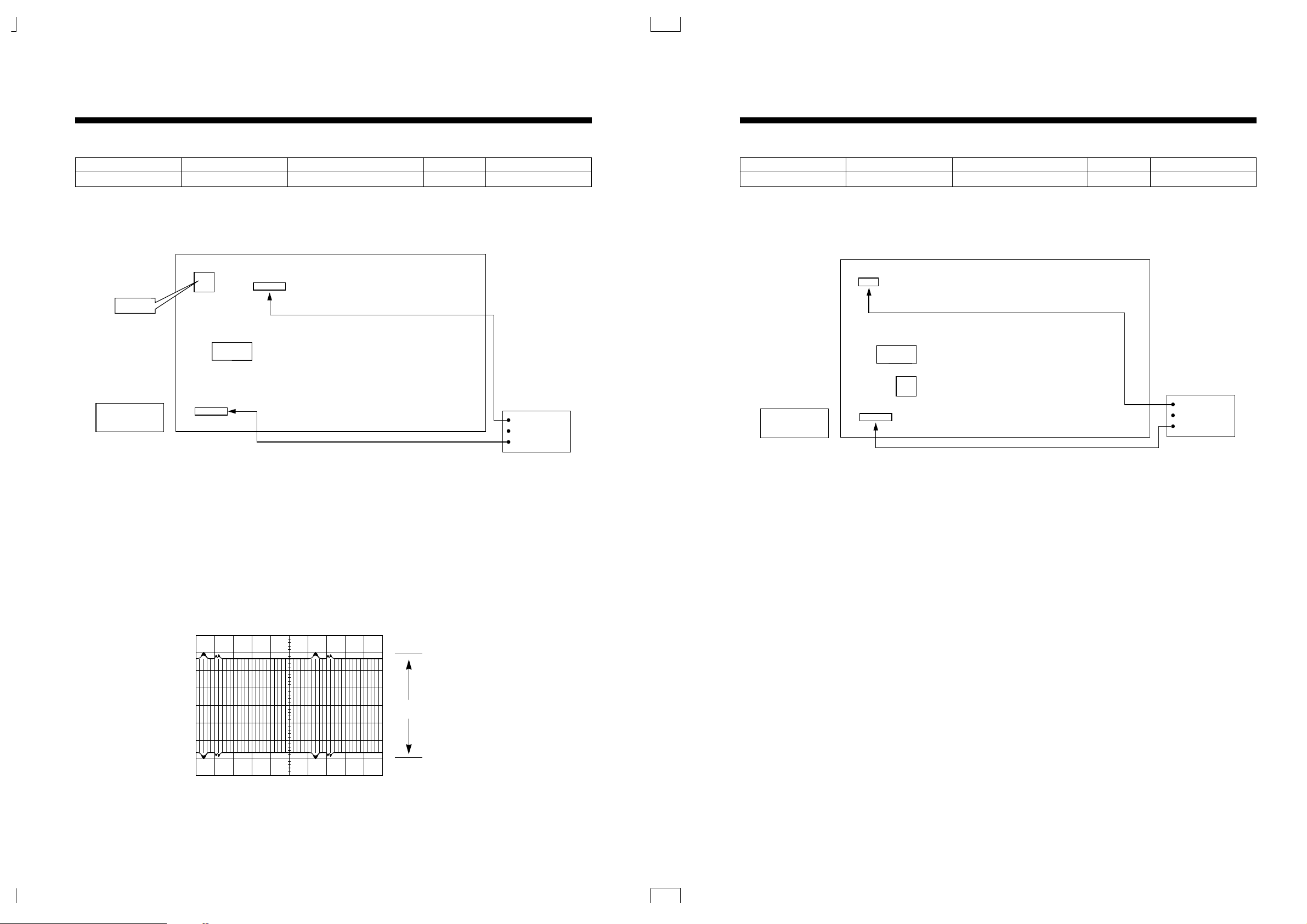
2-1. SERVO CIRCUIT ADJUSTMENT METHOD
1. PLAYBACK PHASE
• Connection Method
• Adjustment Procedure
1) Play back the test tape.(DP-2)
2) Set the oscilloscope to the CHOP mode. Connect CH1 to the SW PULSE (PT01 PIN
3), and CH2 to the VIDEO OUT
(TJ396) and trigger the scope with signal form CH1
3) Adjust R591 to the positive rising edge of SW PULSE at 6.5H ± 0.5H from the V-SYNC
SECTION 2. ELECTRICAL ADJUSTMENT
Adj. Location Checking Point Measuring Equipment Mode Test Tape
TJ396
DP-2
R591
PT01 PIN
3
Oscilloscope Play
Modulator
TJ396
CH-1
OSCILLOSCOPE
CH-2
R591
PT01
TOP VIEW
6.5H 0.5H
+
_
5
Horizontal: 50µs/div
Vertical: 0.5V/div
6.5±0.5H
3. PLAYBACK OUTPUT LEVEL
• Connection Method
• Adjustment Procedure
1) Playback the test tape, DP-1 Color Bar
2) Connect the oscilloscope to TJ396 and trigger the scope externally with C.SYNC signal form TJ313
3) Adjust R396 to obtain 2.0V ± 0.1Vp-p between the SYNC TIP and 100% white.
8
TJ396
R396
TJ313
TOP VIEW
IC301
CH-1
OSCILLOSCOPE
CH-2
PB-Y
Adjustment Parts Checking Point Measuring Equipment Test Tape Input Signal
R396 TJ396, TJ313 Oscilloscope DP-1 – –
2.0Vp-p±0.1Vp-p
TJ 396
Horizontal: 10µs/div
vertical : 0.5v/div
7
2. SYNC TIP FREQUENCY
• Connection Method
• Adjustment Procedure
1) Set the TV/LINE to LINE mode.
2) Supply the input signal in the OPEN state.
3) Set the VCR to STOP mode.
4) Connect the Frequency counter to TJ391
5) Adjust R391 to obtain 3.73±0.1MHz
TJ391
R391
TOP VIEW
IC301
3.73±0.1MHz
+
–
Frequency
Adj. Location Checking Point Measuring Equipment Test Tape Input Signal
R391 TJ391 Frequency Counter – –
5. FM DEVIATION
• Connection Method
• Adjustment Procedure
1) Set the TV/LINE to LINE mode.
2) Supply the Color bar signal with 100% white to the VIDEO IN TERMINAL
3) Record the color bar signal for a few minnutes and play it back
Then confirm that the playback Y-Signal out level is 2.0 ± 0.2Vp-p.
4) If the playback level is not 2.0V ± 0.2Vp-p, adjust the following.
5) Turn the R392 a little. Record the color bar signal for a minute, and confirm the Y-signal output level.
6) Repeat preceding steps until the playback Y-signal level becomes 2.0V±0.2Vp-p between the SYNC TIP and 100%
white level
TJ396
TJ313
TOP VIEW
IC301
CH-1
OSCILLOSCOPE
CH-2
SIGNAL
GENERATOR
R392
10
Adjustment Parts Checking Point Measuring Equipment Test Tape Input Signal
R392 TJ396 Signal Gen, Oscilloscope Blank Tape Color Bar
4. LUMINANCE RECORD CURRENT
• Connection Method
• Adjustment Procedure
1) Set the TV/LINE to LINE mode.
2) Supply the Color bar signal to the VIDEO IN TERMINAL.
3) Set the VCR to the REC mode.
4) Connect CH-1 of oscilloscope to TJ399 and GND, and trigger the oscilloscope with SYNC signal at TJ313
5) Adjust R399 until record current becomes 280 ± 5mVp-p at SYNC TIP of luminance
R399
TJ313
TOP VIEW
IC301
CH-1
OSCILLOSCOPE
CH-2
REC-Y
SIGNAL
GENERATOR
TJ399
9
Adjustment Parts Checking Point Measuring Equipment Test Tape Input Signal
R399 TJ399, TJ313 Signal Gen, Oscilloscope Blank Tape Color Bar
280±5mmVp-p
TJ 399
Horizontal: 10µs/div
vertical : 50mv/div
2-3. AUDIO CIRCUIT ADJUSTMENT METHOD
1. AUDIO RECORD BIAS
• Connection Method
• Adjustment Procedure
1) Set the TV/LINE to LINE mode.
2) Set the input to open mode (Without Audio input)
3) Connect the Audio level meter to both TP1 and TP2
4) After inserting a blank tape, record in SP mode.
5) Adjust R292 to obtain 3.0 mVrms.
12
TOP VIEW
R292
3.0mVrms
+
–
A/CHEAD
TP2
(–)
TP1
(+)
Audio LEVEL METER
Adjustment Parts Checking Point Measuring Equipment Test Tape Input Signal
R292
A/C Head PCB
Audio level meter Blank Tape No signal
TP1(+), TP2(-)
11
6. NTSC COLOR PHASE ADJUSTMENT METHOD
• Connection Method
• Adjustment Procedure
1) Playback the test tape, DN-1 NTSC COLOR BAR.
2) Connect the vector scope to video output.
3) Adjust CN15 to obtain same color burst phase and level both video out signal and burst marker in vector scope.
4) Confirm same color burst phase and level both video output signal and burst marker in vector scope.
ICN01
CN15
NTSC COLOR
PHASE
PN01
Vector
Scope
To SCART JACK
VIDEO OUT
Adjustment Parts Checking Point Measuring Equipment Test Tape Input Signal
CN15 Video Out PAL Vector Scope
DN-1
–
NTSC Color
b
B
mg
CX
G
20%
10%
y1
YL
g
CY
G
120
100
80
60
40
20
0
20
43
0°
10°
10°
14
2-4. IF MODULE CIRCUIT ADJUSTMENT METHOD
1. 32.4 MHZ TRAP (PAL, SECAM-B/G SYSTEM ONLY)
• Connection Method
• Adjustment Procedure
1) Supply +12V to PIN
6 , and GND to PIN 7 of H101
2) Connect the signal generator output to pin
8 and GND to PIN7
3) Connect the oscilloscope to check point
4) Adjust L101 to obtain minimum level at the check point.
•INPUT SIGAL TABLE
13
Adj. Location Checking Point Measuring Equipment Input signal
Q101 Signal gen Refer to
L101 Collector Oscilloscope the
Power supply table on page13.
32.4MHz
S/N : 97P650031A
C111
L110
IC101
R191
L103
C105
Z103
C122
Z102
Q102
C112
L108
L107
H101
1 8
L101
Q101
20
1
11
10
1 5
CH-1
OSCILLOSCOPE
CH-2
OUT
SIGNAL GEN
GND
GND
+12V
POWER
SUPPLY
#8
#7
#6
#7
Q101
collector
#6 #7
#8
Refer to input
signal table on
page 13.
NO Adj item
PAL,SECAM PAL,SECAM
PAL-I PAL-B/H PAL-I/I
-B/G -B/G,D/K
1 32.4MHz 32.4MHz
X
31.5MHz
X
32.4MHz
X
TRAP 80dBµV 80dBµV 80dBµV
TANK fm : X fm : X fm : X fm : X fm : X fm : X
2 RESONA fc : 38.9MHz fc : 38.9MHz fc : 39.5MHz fc : 36.875MHz fc :38.9MHz fc : 38.9MHz
-NT 80dBµV 80dBµV 80dBµV 80dBµV 80dBµV 80dBµV
AFT
fm : 15.625KHz fm : 15.625KHz fm : 15.625KHz fm : 15.625KHz fm : 15.625KHz fm : 15.625KHz
3
Coil
30% AM 30% AM 30% AM 30% AM 30% AM 30% AM
80dBµV 80dBµV 80dBµV 80dBµV 80dBµV 80dBµV
fm : 15.625KHz fm : 15.625KHz fm : 15.625KHz fm : 15.625KHz fm : 15.625KHz fm : 15.625KHz
4
RF 30% AM 30% AM 30% AM 30% AM 30% AM 30% AM
AGC 98dBµV
(HYPER BAND)
98dBµV 92dBµV 95dBµV 92dBµV 98dBµV
92dBµV
(WIDE BAND)
• HYPER BAND
TUNER : TEKE4-005B(120A)
TUNER : CSR1A749 TUNER : VTSS7SZ3
DT2-BV08P
5 REMARKS IF : 97PB204000 IF : 97PB209100 IF : 97PB207200
• WIDE BAND
TUNER : VTSS7SZ3
IF : 97PB207200
2. TANK RESONANT
• Connection Method
• Adjustment Procedure
1) Supply +12V to PIN
6 , and GND to PIN 7 of H101
2) Connect the signal generator output to pin
8 and GND to PIN7
3) Connect the oscilloscope to check point
4) Adjust L109 to obtain minimum DC voltage at the check point.
S/N : 97P650031A
C111
L110
IC101
R191
L103
C105
Z103
C122
Q102
C112
H101
1 8
L101
Q101
1
11
10
1 5
CH-1
OSCILLOSCOPE
CH-2
OUT
SIGNAL GEN
GND
GND
+12V
POWER
SUPPLY
#8
#7
#6
#7
#6 #7
#8
minimum
#5
Carrier : Refer to input
signal table
on page 13.
Adj. Location Checking Point Measuring Equipment Input signal
H101 Signal gen Refer to
L109 PIN
5 Oscilloscope the
Power supply table on page13.
1615
3. AFT COIL
• Connection Method
• Adjustment Procedure
1) Connect the TEST circuit to PIN
2 of H101
2) Supply +12V to pin
6 and GND to PIN 7 of H101
3) Connect the signal Generator output to PIN
8, and GND to PIN 7
4) Connect the oscilloscope to check point
5) Adjust L110 to obtain 2.3V ± 0.15V DC at “A” point DC Voltage change rapidly.
S/N : 97P650031A
C111
L110
IC101
R191
L103
C105
Z103
C122
Q102
C112
H101
1 8
L101
Q101
1
11
10
1 5
CH-1
OSCILLOSCOPE
CH-2
±12V
POWER SUPLLY
GND
2.3V±0.15V
OUT
SIGNAL GEN
GND
VCC+12V
43K
33K
18K
"A"
0.01µF
0.47µF
/50V
TEST CIRCUIT
#8
#7
"A"POINT
#8
#7
#6#2
#6
#7
#2
l102
Carrier : Refer to input
signal table
on page 13.
+
Adj. Location Checking Point Measuring Equipment Input signal
Signal gen Refer to
L110 “A” Point Oscilloscope the
Power supply table on page13.
4. RF AGC
• Connection Method
• Adjustment Procedure
1) Supply +12V to PIN
6 , and GND to PIN 7 of H101
2) Connect the signal generator output to pin
8 and GND to PIN7
3) Connect the oscilloscope to check point
4) Adjust R191 to obtain 6.0 ± 0.2V DC at check point.
S/N : 97P650031A
C111
L110
IC101
R191
L103
C105
Z103
C122
Q102
C112
H101
1 8
L101
Q101
1
11
10
1 5
CH-1
OSCILLOSCOPE
CH-2
OUT
SIGNAL GEN
GND
GND
+12V
POWER
SUPPLY
#6
#7
#6 #7
#8
#1
Z102
L108
L107
20
Carrier : Refer to input
signal table
on page 13.
Adj. Location Checking Point Measuring Equipment Input signal
H101 Signal gen Refer to
R191 PIN
1 Oscilloscope the
Power supply table on page13.
18
Check each voltage on
M801(SMPS Modute)
Check voltage
C851, C856,
C853, C855
Change of the M801
NO
Check D851, D854, Q851, Q852
NO
Check the main
PCB circuit (+6V) &
Logic PCB circuit (-24V)
YES
YES
B. CHECKING THE SECONDARY CIRCUIT. (Before secondary circuit open).
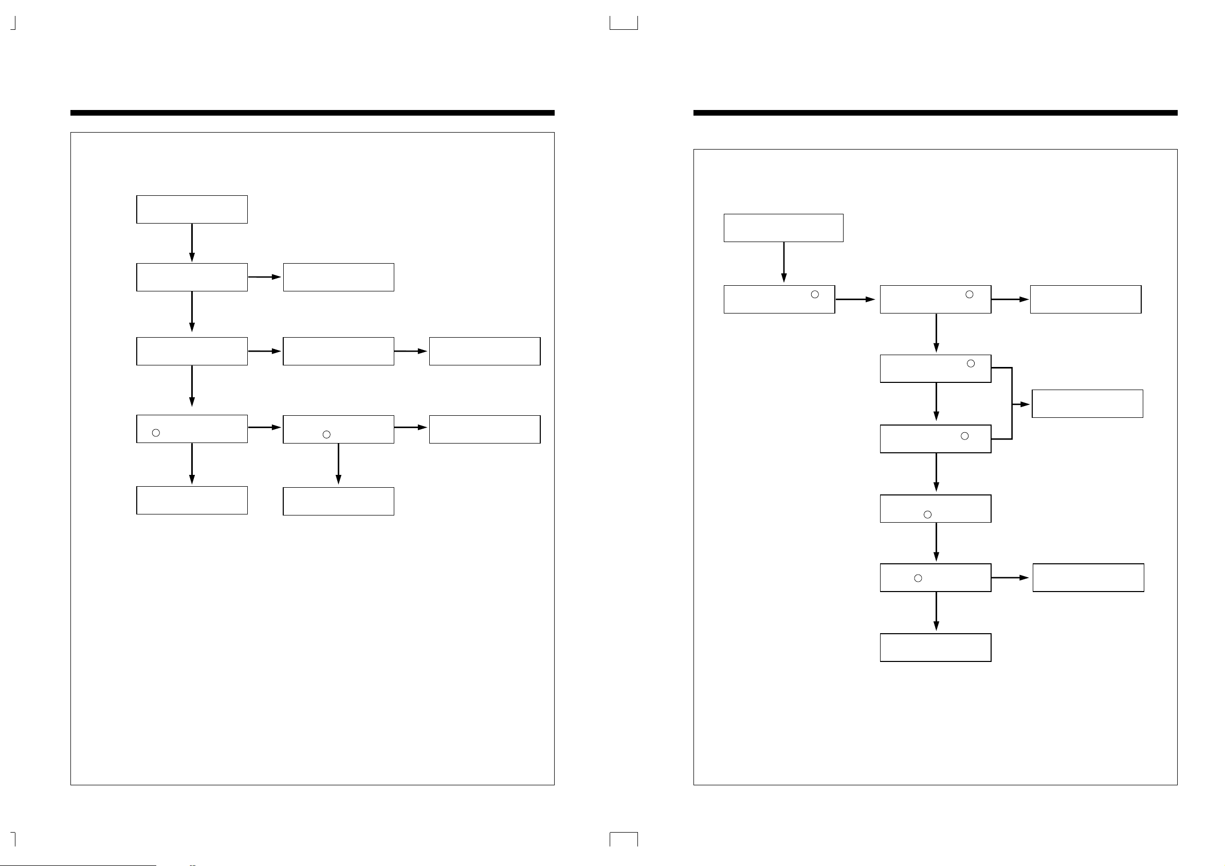
SECTION 3. TROUBLE SHOOTING FLOW CHART
3-1. POWER CIRCUIT
• When changing the parts which are out of order, first, remove the power plug from the socket and then discharge the
voltage across between both terminals of C807. (Use an external approximately 20KΩ resistance)
• When check the primary circuit by using the oscilloscopes insulate the oscilloscope properly (Use the isulating
transformer) and GND must be connected GND into the primary GND (But there is no connection when checking the
secondary circuit).
• When changing M801, check FUSE and Cement resistance properly.
17
Prepare the instrument
connecting the insulating trans.
Check F801 FUSE.
Is voltage applied to D801?
Is voltage applied to the
both terminals of C807?
Check D801, L801 & L802.
Check R802 &
M801(SMPS Module)
Check the Secondary circuit.
NO
NO
YES
YES
YES
YES
YES
NO output Voltage.
A. CHECKING THE PRIMARY CIRCUIT.
20
Digitron is lit but keys do
not operate.
Is each key pulse
applied to pin ,
and of IC701?
2 3
12 13
Check key matrix
circuit.
Check the pin serial of
pin , , , of IC701.
24
Power compensation
does not operated.
When mains is
unplugged is 3.6V at
pin and of IC601?
26 81
Is signal applied to
pin and of IC601?
42 43
Check IC601.
Check C623.
Check x602.
NO
YES
YES
YES
YES
NO
NO
B.
C.
YES
23 22 21
B.
C.
3-2. LOGIC CIRCUIT
19
Digitron does
not operate.
Is+5V supplied to
pin of IC701?
8
Is-24 V supplied to
pin of IC701?
11
Are -20 and -16.5V
supplied to pin and
of G701?
1
35
Are CLK signals
supplied to pin ,
and of IC701?
1 2
3
Is 5V at pin of
IC701?
7
Check X701
Change IC701
Check M801
Is+6V supplied
from D713 cathod
Change IC701
Change X701
YES
YES
YES
YES
YES
YES
NO
NO
NO
NO
A.
YES
Check M801
NO
Check M801
NO
Check IC601
NO

22
Playback picture
is not good.
Noise appears
on the screen
on the whole.
Is Enve.wavefrom
supplied to pin of
PT01
4
Are SW pulse and
HA SW applied to
PreAmp circuit?
Check video circuit.
Auto stop during
playback.
Is Reel pulse
applied to pin and
of IC601?
5
6
Check flow A
Is SW pulse obtained
from pin of IC601?
16
Check D.PG input
and connector
between deck and
main PCB.
Check pattern
Check connector, Head
Amp and Head dust.
Change head
Check reel sensor.
Is D.FG applied to
pin of IC601
Check connector and
D.FG circuits.
Check IC601.
YES
NO
YES
YES
YES
YES
YES
YES
NO NO
NO
NO
NO
YES
NO
67
B.
C.
21
91
The voltage of pin
of IC601 is not
changed.
Is CTL pulse input
to pin and of
IC601
71 72
73
Check and
re-adjust the
Path of Deck.
Check circuit
adjacent to IC601.
Check R668, R669
C508, C509.
Check R518
and C511.
Check IC601
YES
YES
YES
YES
YES
YES
YESNO
NO NO
NO
NO
A.
Playback picture
is not good.
Noise appears
although adjusting
tracking.
Is CTL pulse applied
to pin of IC601.
Noise shakes up
and down on the
screen.
CTL HEAD height is
normal and there is
not dust.
Adjust the HEAD
height and remove
dust.
Noise appears
although change
cassette tape.
YES
3-3. SERVO SYSCON CIRCUIT
24
Drum M/T and Capstan M/T rotate
at regular speed. (In REC mode)
Is C. Sync applied to
pin of IC601?
93
Check Motors.
Check C. Sync of
VIDEO IC and Pattern
Emergency mode appears when plugging in.
(Power cord)
Is EVER 5V supplied?
Are CAM SW DATA Correct?
Check IC602.
Check IC 601.
Check power circuit.
Recheck connector
and CAM SW contact.
NO
YES
YES
YES
YES
NO
NO
NO
F.
G.
YES
23
Drum M/T loading stops.
Is Drum Motor 12V at
pin of P601 supplied?
Is pin D.FG of
IC601 supplied.
Is D.PWM (pin )
of IC601 supplied?
Check connector (P601)
and drum Motor.
Is pin of P501
input to 2V-3.5V?
Is pin of P601 2.5V?
Is pin (C.PWM)
of IC601 Supplied?
Check connector (P501)
and capstan Motor.
67
4
1
18
3
Check Q851 of
power circuit.
Check C505, R506, R507
and C516
Check IC601
Check D854 of power circuit.
Check circuit of R510,
R511, R512.
Check R508, R509
Check IC601
YES
YES
YES
YES
YES
YES
YES
YES
NO
NO
NO
NO
NO
NO
NO
Capstan M/T loading stops.
Is capstan Motor 12V
at pin of P501 supplied?
D.
E.
5
8
1
3-4. AUDIO CIRCUIT
26
No sound in the playback mode.
22
Is the output at pin
of IC201?
Is 9V applied to pin
of IC201?
Check Q204 and
power circuit.
7
Is 5V applied to pin
of IC201?
11
Is applied to pin
9V of IC201
24
Is there Audio output
at pin of IC201?
10
Is pin of IC201 GND?
3
Check Pattern
and AC Head.
Check IC601.
Check IC201
NO
YES
NO
YES
YES
YES
YES
NO
NO
NO
A
25
Cassette is not
inserted.
Is drum Motor 12V supplied?
Check Q851 of power
circuit
CAM DATA are changed
when CST IN?
Is 5V applied to
pin of IC602 when CST IN?
4
Chek IC602
Check connector. Check DECK part.
Is 5V supplied at
pin of IC601?
Check PATTERN
45
Check IC601
H.
NO
YES
YES
YES
NO NO
NO NO
YES
YES
3-5. VIDEO CIRCUIT
28
Is video signal input
into pin and of IC151?
12 13
Is E12V supplied to
pin of IC151
16
Is signal output from
pin of IC151?
14
Is signal input into
pin of IC301?
31
Is signal output from
pin of IC301?
28
Check PIF circuit
and A/V jack.
Check ever 12V
Check IC151 and
adjacent circuit.
Check connector and
PCB pattern
Is 5V supplied to pin
and of IC301?
24
29
Check
power circuit
Check IC301
pin EE(L)/PB(H)
Check
IC601 pin
29
Change IC301
Is signal input from
ICS01 pin?
10
Is signal output from
ICS01 pin?
8
Check pattern,
connector and Q312.
Check osd circuit
RF out Line out
YES
YES
YES
YES
YES
YES
YES
YES
NO
NO
NO
NO
NO NO
H
L
A.EE MODE PIcture N.G
NO
YES
4
27
No sound in the playback
mode after in the record mode.
Is the signal applied to
pin of IC201?
16
Is 5V applied to
pin of IC201?
24
Is there output at
pin of IC201?
21
Does T201 oscillate?
Check circuit adjacent
to IC151.
Check IC601.
Check IC201.
Is the voltage above 10V
at pin of T201
Check Q201
collector:above 10V
Base:0V
Check T201
Is record current
3.0mVms?
Is 0V applied to
pin of IC201?
Clean HEAD.
Adjust Record current.
Check IC201.
Check Q202 and T201.
Check Q201.
NO
YES
YES
YES
YES
YES
YES
NO
NO
NO
YES
NO
NO
NO
NO
YES
3
B
1
30
7
Is envelope output
ICA 01 pin?
Is signal input to
IC301 pin?
Is signal output
from IC301 pin
Is signal input
to IC301 pin?
Is color signal input
to IC301 pin?
Is composite video signal
output from IC301 ?
Check OSD circuit
33
2
3
21
28
Is on/off 5V supplied to
ICA 01 , pin?
Is sw pulse input to
ICA 01 , pin?
Check QA01,
QA02, QA03
Check IC301
vcc , pin
Check power
circuit
Check IC601
pin
Change IC301
Check IC301
pin EE(L)/PB(H)
Check Q302, 303
Check QA04, QA05
Is C.signal input
to IC301 pin?
Is color signal input
to IC301 pin?
23
Check X402 and
adjacent circuit.
Change IC301
1 2
4 5
Check power
circuit
Check IC601
, pin
Claen head or
change head
17 18
29 24
4
29
14
NO
YES
YES
YES
YES
YES
YES
YES
NO
NO
YES
NO
NO
YES
YES
NO
NO
YES
NO
NO NO
NO
YES
C. PB VIDEO SIGNAL N.G
NO
11
29
Is 5V supplied to ICS01 and pins?
Check oscillation of ICS01 and pins.
Check serial data (ICS01 pins)
Change ICS01 and check OSD circuit.
Check ON/OFF +5V
Check XS01 (17.7MHz)
Check IC601.
3
16
4 5
YES
YES
NO
NO
NO
B . OSD Character N.G
20 7
YES
17
31
Check EE mode
34
Is luminance and color
signal output
from IC301 , pin?
Is signal input to
IC301 pin?
Is rec signal input
to ICA01 , , pin?
Check video head and
connector
Check A/V SW CIRCUIT
Is +5V supplied to
ICA01 , pin
Is rec signal input
to ICA01 pin?
Check Q308, Q310
Check power circuit
14
12
13 14 15
1 2
31
NO
YES
YES
YES
YES
NO
YES
NO
NO NO
D. REC SIGNAL N.G
SECTION 5. CIRCUIT DIAGRAM
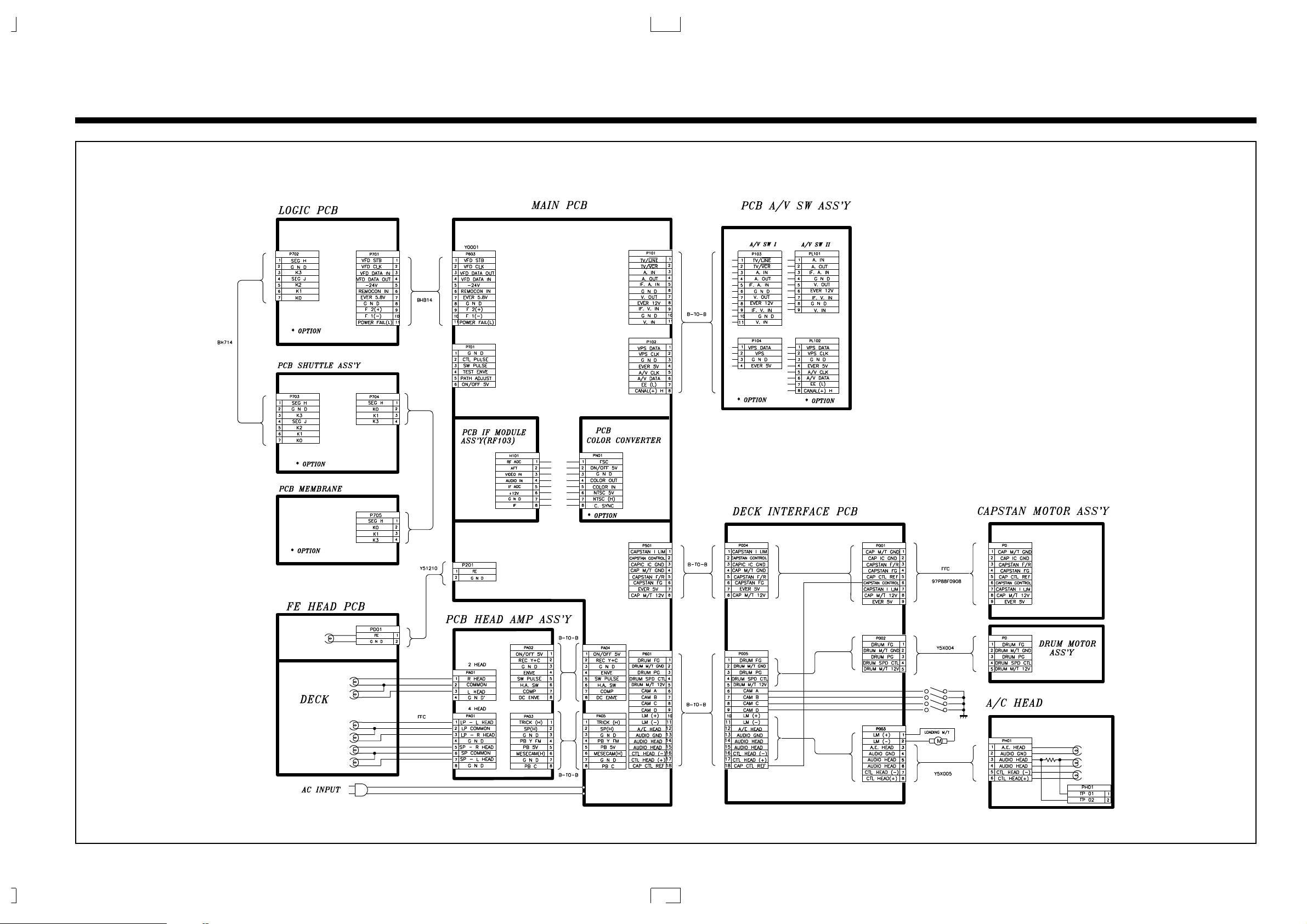
5-1. CONNECTION DIAGRAM CIRCUIT
33
 Loading...