


DAEWOO DV-K10DY-QB-E, DV-K12DY-QB-E, DV-K10DY-QB-D, DV-K12DY-QB-D, DV-K12D-QB-D Service Manual
...
Service Manual
MODEL : DV-K10DY-QB/E
DV-K12DY-QB/E
DV-K10DY-QB/D
DV-K12DY-QB/D
DV-K12D-QB/D
DV-K10DZ-QB/D
DV-K10P-QB
=
DV-K10W
BLUE DIAMOND II #
NTSC PLAY BACK ON PAL TV
POWER
|
|
|
|
FF |
CASSETTE IN REW |
PLAY |
FF |
RECORD |
PLAY |
STOP/EJECT |
|
|
|
|
|
|
|
|
REW |
INFRARED |
REMOTE SENSOR |
DAEWOO ELECTRONICS CO., LTD.

SPECIFICATIONS
GENERAL
Power requirement |
AC90~260V, 50/60Hz |
Power consumption |
Typical 10W |
Temperature |
5¡C~35£ ¡C£ (Operating) |
|
-20 C~60 C |
|
(Storage temperature) |
Operating position |
Horizontal only |
Dimensions (WxHxD) |
280x90x345 (mm) |
Weight |
Approx 3.6kg |
Format |
VHS standard |
Tape widch |
12.65mm |
Tape speed |
(SP): 23.39mm/sec |
Maximum recording time |
|
with full-size cassette |
(SP): 240 min. with E-240 |
Maximum recording time |
video cassette |
|
|
with full-size cassette |
(SP): 45 min. with E-45 |
|
cassette |
VIDEO
Signal system |
PAL colour and CCIR |
|
|
monochrome signals, |
|
|
625 lines/50 fields |
|
Recording system |
Rotary two-head helical scan |
|
|
with a slant double-azimuth |
|
|
combination video head |
|
Input |
1.0Vp-p, 75 ohms, unbalanced |
|
Output |
1.0Vp-p, 75 ohms, unbalanced |
|
Simal to noise rallio |
45 dB (Rohde & Schwarz |
|
|
noise mater) with NETTETE |
|
|
IMAGE contol |
at centre |
|
position |
|
Horizontal resolution |
240 lines with |
NETTETE |
|
IMAGE control at centrne |
|
|
pomition |
|
AUDIO
Input |
-8 dBs, (CENELEC standard) |
|
more than 47 k-ohms, |
|
unbalanced |
Output |
-6 dBs, (CENELEC standard), |
|
less than 1 k-ohm, unbalanced |
|
(100 k-ohms, load) |
Frequency range |
100 Hz to 8,000 Hz |
Signal to noise ratio |
38 dB (More than) |
Audio Distortion |
Less than 3% (SP) |
RF Output |
UHF channel 36 |
|
(Adjustable 30~39) |
ACCESSORIES
Provided Accessories |
Remote control unit |
|
RF Cable, Battery |
• Design and specifications can be subjected to change without notice.
• Safety Check after Servicing
Examine the area surrounding the repaired location for damage or deterioration. Observe that screws, parts and wires have been returned to original positions. Afterwards, perform the following tests and confirm the specified values in order to verify compliance with safety standards.
1.Insulation resistance test
Confirm the specified insulation resistance or greater between power cord plug prongs and externally exposed parts of the set (RF terminals, antenna terminals, video and audio input and output terminals, microphone jacks, earphone jacks, etc.). See table below.
2.Dielectric strength test
Confirm specified dielectric strength or greater between power cord plug prongs and exposed accessible parts of the set (RF terminals, antenna terminals, video and audio input and output terminals, microphone jacks, earphone jacks, etc.) See table below.
3.Clearance distance
When replacing primary circuit components, confirm specified clearance distance (d), (d') between soldered terminals, and between terminals and surrounding metalic parts. See table below.
d
Primary circuit termimals
d'
Chassis 
a
Table 1: Rating for selected areas |
|
Fig. 1 |
|
||
|
AC Line Voltage |
Region |
Insulation |
Dielectric |
Clearance |
|
Resistance |
Strength |
Distance (d), (d') |
||
|
|
|
|||
|
100V |
Japan |
≥ 1 MΩ /500 V DC |
1kV AC 1 minute |
≥ 3 mm |
|
110 to 130V |
USA & |
– – – |
900V AC 1 minute |
≥ 3.2mm |
|
Canada |
||||
|
|
|
|
|
|
|
* 110 to 130 V |
Europe |
≥ 4 MΩ /500 V DC |
3 kV AC 1 minute |
≥ 6 mm (d) |
|
200 to 240 V |
Australia |
|
|
≥ 8 mm (d') |
|
|
|
|
|
(a: Power cord) |
* Class II model only.
Note: This table is unofficial and for reference only. Be sure to confirm the precise values for your particular country and locality.
4.Leakage current test
Confirm specified or lower leakage current between B (earth ground, power cord plug prongs) and externally exposed accessible parts (RF terminals, antenna terminals, video and audio input and output terminals, microphone jacks, earphone jacks, etc.)
Measuring Method: (Power ON) |
|
|
|
|
Exposed |
|
|||
|
|
|
|
accessible |
|
||||
Insert load Z between B (earth ground, power cord plug |
AC Voltmter |
||||||||
part |
Z |
||||||||
prongs) and exposed accesible parts. Use and AC |
|
(high impedance) |
|||||||
voltmeter to measure across both terminals of load Z. |
|
Earth Ground |
|||||||
See figure 2 and following table. |
|
|
|
||||||
|
|
|
B power cord plug prongs |
||||||
|
|
|
|
|
|
|
|||
|
|
|
|
|
|
||||
Table 2: Leakage current ratings for selected areas |
|
|
|
Fig. 2 |
|
||||
|
|
|
|
|
|
|
|
|
|
AC Line Voltage |
|
Region |
|
Load Z |
Leakage Current (i) |
Earth Ground |
|||
|
|
(B) to: |
|||||||
|
|
|
|
|
|
|
|
||
|
|
|
|
|
|
|
|
|
|
100V |
|
Japan |
|
|
|
¡ ≤ 1m A rms |
Exposed accessible |
||
|
|
1k |
parts |
||||||
|
|
|
|
|
|
||||
110 to 130 V |
|
USA & |
|
1.5kµF |
¡ ≤ 0.5 m A rms |
Exposed accessible |
|||
|
|
|
|
||||||
|
|
|
|
1.5k |
|
|
parts |
||
|
|
|
|
|
|
¡ ≤ 0.7 m A peak |
Antenna earth |
||
110 to 130 V |
|
Europe |
|
2k |
|
¡ ≤ 2 m A dc |
terminals |
||
200 to 240 V |
|
Australia |
|
|
|
¡ ≤ 0.7 m A peak |
Other terminals |
||
|
|
|
|
50k |
|
¡ ≤ 2 m A dc |
|||
|
|
|
|
|
|
||||
Note: This table is unofficial and for reference only. Be sure to confirm the precise values for your particular country and locality.

TABLE OF CONTENTS
SECTION 1. CONTROLS AND FUNCTIONS.......................................................................................................... |
2 |
SECTION 2. ELECTRICAL ADJUSTMENTS |
|
2-1. SERVO CIRCUIT ADJUSTMENT METHOD ..................................................................................................................... |
3 |
2-2. AUDIO CIRCUIT ADJUSTMENT METHOD...................................................................................................................... |
4 |
SECTION 3. TROUBLE SHOOTING FLOW CHART |
|
3-1. POWER CIRCUIT............................................................................................................................................................... |
5 |
3-2. SERVO-SYSCON CIRCUIT............................................................................................................................................... |
7 |
3-3. AUDIO CIRCUIT............................................................................................................................................................... |
13 |
3-4. VIDIO CIRCUIT ................................................................................................................................................................ |
15 |
SECTION 4. WAVEFORMS ON VIDEO, MAIN CIRCUIT ................................................................................ |
22 |
SECTION 5. µ-COM PORT............................................................................................................................................. |
24 |
SECTION 6. CIRCUIT DIAGRAM................................................................................................................................ |
26 |
6-1. CONNECTION DIAGRAM ............................................................................................................................................... |
26 |
6-2. POWER CIRCUIT DIAGRAM .......................................................................................................................................... |
27 |
6-3. SCART/MAIN CIRCUIT DIAGRAM ................................................................................................................................. |
28 |
6-4. VIDEO & HEAD-AMP ....................................................................................................................................................... |
29 |
6-1. AUDIO CIRCUIT DIAGRAM............................................................................................................................................. |
30 |
SECTION 7. COMPONENTS LOCATION GUIDE ON PCB BOTTOM VIEW........................................ |
31 |
SECTION 8. SECTION EXPLODED VIEWS AND PARTS LIST ................................................................... |
32 |
8-1. PACKING ASSEMBLY (DV-K10D).................................................................................................................................. |
32 |
8-2. APCKING ASSEMBLY (DV-K12D).................................................................................................................................. |
33 |
8-3. CHASSIS ASSEMBLY (DV-K10D) .................................................................................................................................. |
34 |
8-4. CHASSIS ASSEMBLY (DV-K12D) .................................................................................................................................. |
35 |
SECTION 9. ELECTRICAL PARTS LIST.................................................................................................................. |
36 |
SECTION 10. OPTION TABLE...................................................................................................................................... |
43 |
1
SECTION 1. CONTROLS AND FUNCTIONS
FRONT
DV-K10W
=
DV-K10W
BLUE DIAMOND II #
NTSC PLAY BACK ON PAL TV
POWER
|
|
|
|
FF |
CASSETTE IN REW |
PLAY |
FF |
RECORD |
PLAY |
STOP/EJECT |
|
|
|
|
|
|
|
|
REW |
INFRARED |
REMOTE SENSOR |
DV-K12W
=
DV-K12W
|
|
BLUE DIAMOND II # |
|
|
|
|
|
NTSC PLAY BACK ON PAL TV |
|
|
|
POWER |
STOP/EJECT |
REW |
|
|
|
PLAY |
|
|
|
||
|
|
CST IN |
FF |
REC |
|
|
|
REW |
REAR
RF OUT
CH.H  CH.L
CH.L
EURO-AV
K |
ANT. IN |
G
ON  TEST
TEST
OFF
|
|
RF OUT |
|
CH.H CH.L |
VIDEO AUDIO |
||
|
|
||
K |
|
IN |
|
|
ANT. IN |
||
G |
TEST |
OUT |
|
ON |
|||
|
|
||
OFF |
|
|
|
2
SECTION 2. ELECTRICAL ADJUSTMENT
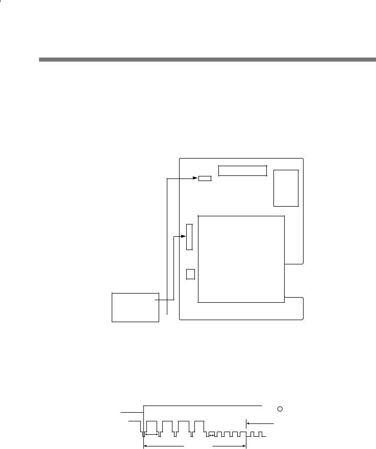
2-1. SERVO CIRCUIT ADJUSTMENT METHOD
1. VIDEO HEAD SWITCHING POSITION
Adjustment Parts |
|
Checking Point |
Measuring Equipment |
Mode |
Test Tape |
R592 |
|
R307 |
Oscilloscope |
PLAY |
DP-2 |
|
PT01 PIN ¤Ø |
||||
• Connection Method |
|
|
|
|
|
|
|
|
|
|
|
• Adjustment Procedure |
|
|
|
|
|
Modulator
P S
O M
R307 W P
E S
R
PT01 PIN3
DECK
R592
CH-1
OSCILLOSCOPE
CH-2
1)Play back the test tape.(Color Bar DP-2)
2)Set the oscilloscope in the chop mode connect the CH1 to SW pulse(PT01 PIN#), the CH2 to VIDEO OUT(R307 ) with CH1 triggering.
3)Adjust R592 for the positive trigger unitill 6.5±0.5H cycles before the vertical SYNC pulse.
CH1 |
|
SW 30Hz |
|
|
|
(PT01 |
3 |
PIN) |
|
|
|
VERTICAL SYNC |
|
|
CH2 |
|
|
|
|
|
1H |
(R307) |
|
|
|
0.5H |
|
|
|
|
|
|
|
|
|
|
6.5H ± 0.5H |
|
|
|
TRIGGER |
|
|
|
3
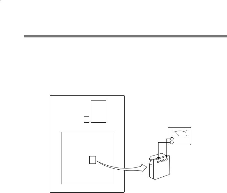
2-2. AUDIO CIRCUIT ADJUSTMENT METHOD
1. AUDIO RECORD BIAS
Adjustment Parts |
Checking Point |
Measuring Equipment |
Test Tape |
Input Signal |
|
R292 |
A/C Head PCB |
Audio level meter |
Rec |
None signal |
|
R01 |
|||||
|
|
|
|
||
|
|
|
|
|
|
• Connection Method |
|
|
|
|
P S
O M
R292 W P
E S
R
DECK ASSY
A/C HEAD
• Adjustment Procedure
1)Set the power on mode.
2)Set the input to open mode
3)Connect the Audio level meter to both R01
4)After inserting a blank tape, record in SP mode.
5)Adjust R292 to obtain 3.0 mVrms.
Audio LEVEL METER
+
–
A/CHEAD
R101
4
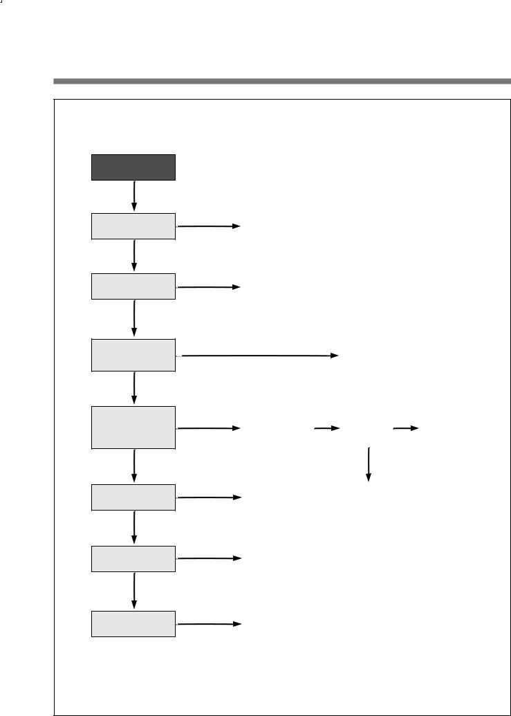
SECTION 3. TROUBLE SHOOTING FLOW CHART
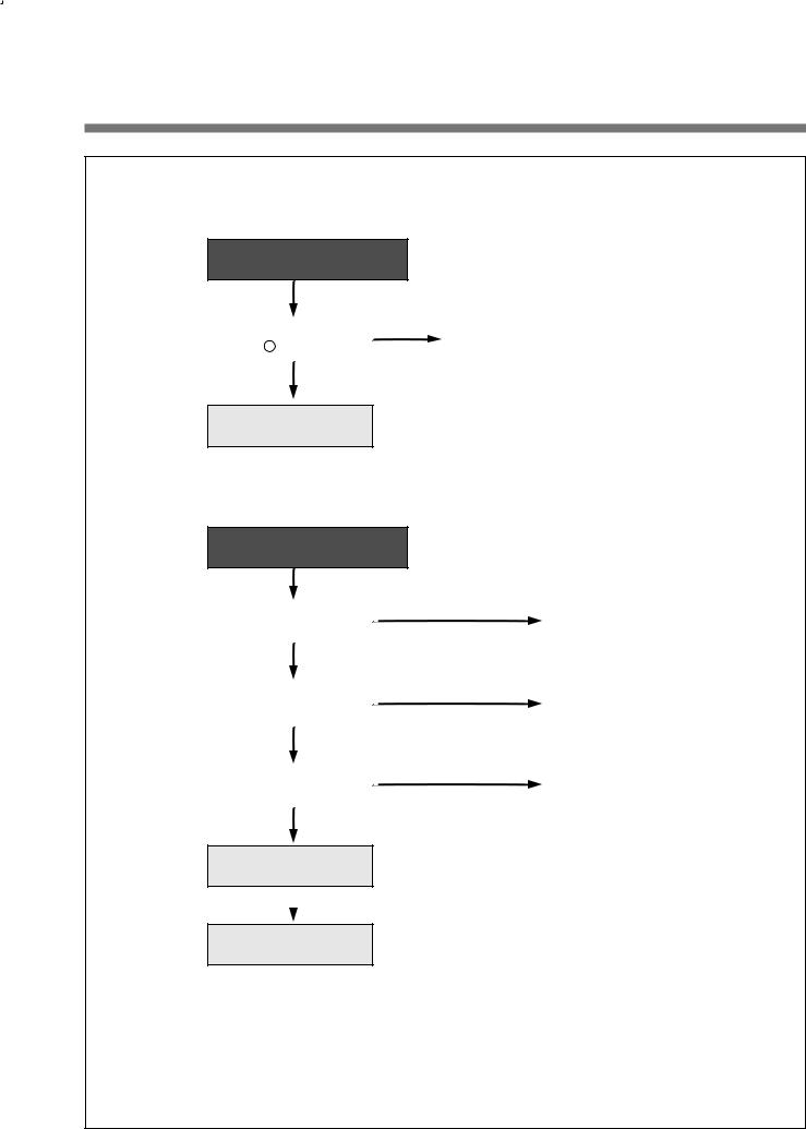
3-1. POWER CIRCUIT
•When change the parts which are out of order, first, remove the power plug from the socket and then discharge the voltage across between both terminals of C807. (Use an external scores of KΩ resistance)
•When check the primary circuit by using the oscilloscopes insulate the oscilloscope surely. (Use the isulating transformer) and must connect GND into the primary GND), (But there is no connection when check the secondary circuit).
•When change IC801, check FUSE and Cement resistance surely.
A. CHECKING THE PRIMARY CIRCUIT.
NO output Voltage |
|
|
|
|
|
|
|
YES |
|
|
|
|
|
|
|
Prepare the instrument |
|
|
|
connecting the insulating trans. |
|
|
|
|
|
|
|
YES |
|
|
|
|
|
|
|
Check F801 FUSE |
|
|
|
|
|
|
|
YES |
|
|
|
|
NO |
|
|
Is voltage applied to D801? |
Check D801, L801 & L802 |
||
|
|||
|
|
|
|
YES |
|
|
|
|
NO |
|
|
Is voltage applied to the |
Check R802 |
||
both terminals of C807? |
|
||
|
|
||
|
|
|
|
YES |
|
|
|
|
|
|
|
Check power module |
|
|
|
|
|
|
5
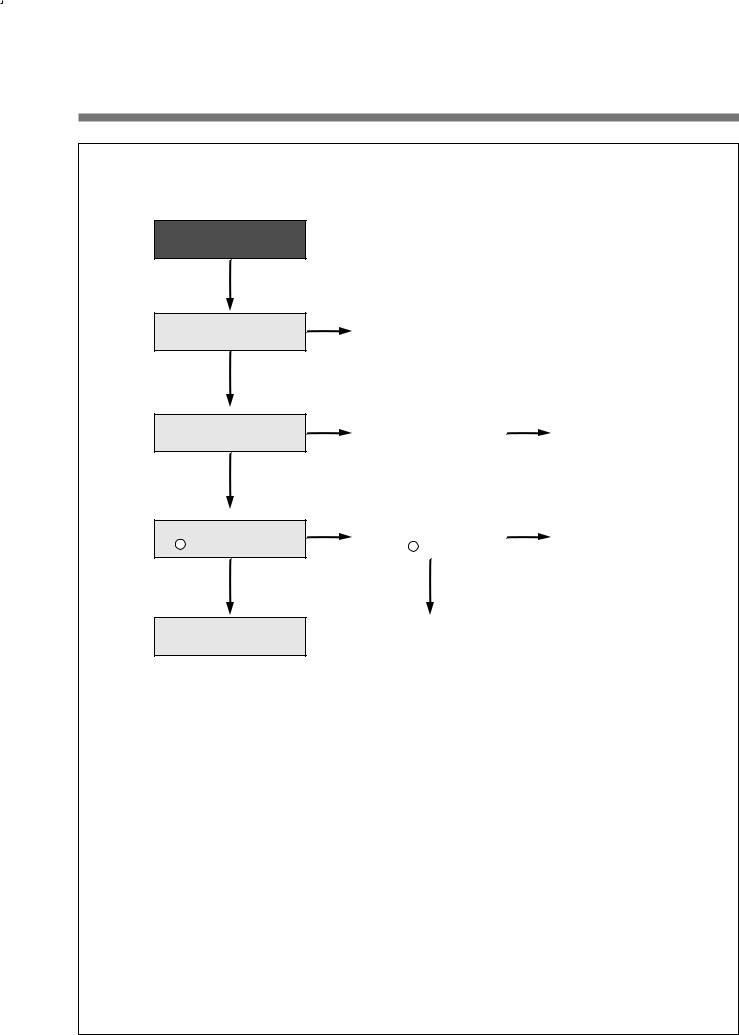
B. POWER MODULE (M801) CHECK
No Voltage
output
Is voltage supplied
Via CN11?
YES
The voltage of #1 of
IC11 is 5.7V and stable
NO
The voltage of #1 of IC11 fluctuate
in 4.8V~5.7V
YES
Measure resistance between GND of CN21 and each terminal
of CN21
Resistance >> 100
The 12DC of each wire of T11 is ok
YES
Primary parts is ok
YES
Secondary parts ok
NO |
Check F801, L801, |
|
L802, D802 |
|
|
YES |
Check the secondary |
|
circuit |
|
|
NO |
Check the pattern |
|
and T11, L12, IC11 |
|
|
|
Terminal open and |
|
The voltage |
NO |
Check the |
|
|
measure the output |
|
parts outside |
|||
|
|
is ok |
|
|
||
|
Voltage |
|
|
|
module |
|
|
|
|
|
|
||
|
|
|
|
|
|
|
|
|
|
YES |
|
|
|
NO |
|
|
|
|
|
|
Change T11 |
|
Check the Diode, |
|
|
||
|
|
Condenser inside |
|
|
||
|
|
|
|
|
||
|
|
|
Module |
|
|
|
|
|
|
|
|
||
|
|
|
|
|
|
|
NO |
Change parts |
|
|
|
out of order |
|
|
NO |
Change parts |
|
|
|
out of order |
|
|
6
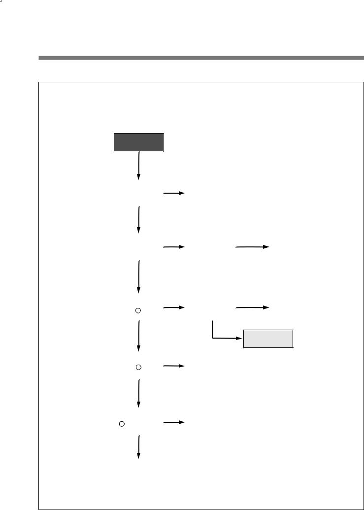
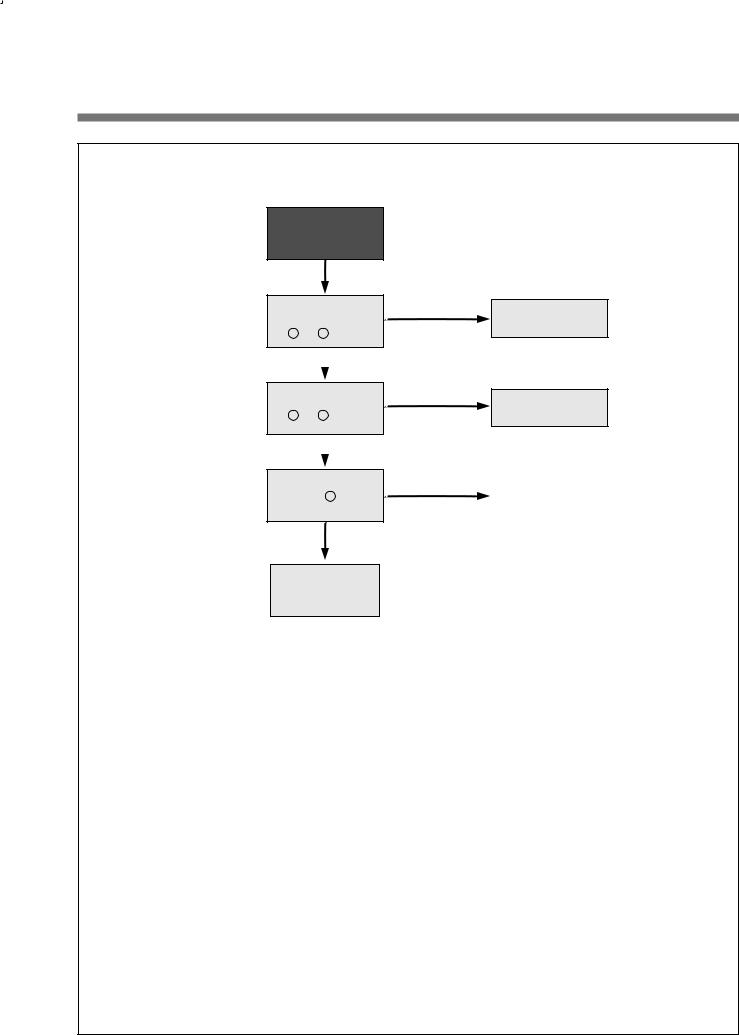
3-2. SERVO SYSCON CIRCUIT
A.
Playback picture is not good.
|
Noise appears |
NO |
|
|
|
|
|
Adjust |
|
||||
although adjusting |
|
tracking |
|
|||
|
tracking. |
|
|
|||
|
|
|
|
|
||
|
|
|
|
|||
|
|
|
|
|
|
|
|
YES |
|
|
|
|
|
|
|
|
||||
Noise shakes up |
NO |
Noise appears |
||||
|
and down on the |
although change |
||||
|
|
|||||
|
screen. |
|
cassette tape. |
|||
|
|
|
|
|
|
|
|
YES |
|
|
|
|
|
|
|
|
|
|
|
|
|
Is CTL pulse out |
NO |
CTL HEAD height is |
|||
from pin 20 of IC601. |
|
normal and there is |
||||
|
not dust. |
|||||
|
|
|
|
|||
|
|
|
|
|
|
|
|
YES |
|
YES |
|||
|
|
|
|
|
|
|
Is CTL pulse input |
NO |
Check C501, C502, |
||||
|
to pin 7 IC601 |
|
C503 |
|||
|
|
|
|
|||
|
|
|
|
|
|
|
|
YES |
|
|
|
|
|
|
|
|
|
|
|
|
The voltage of pin |
|
|
|
|
||
NO |
check R636 |
|
|
|||
|
56 of IC601 is not |
|
|
|||
|
changed. |
|
|
|
|
|
|
|
|
|
|||
|
YES |
|
|
|
|
|
|
|
|
|
|
|
|
|
Check IC601 |
|
|
|
|
|
|
|
|
|
|
|
|
YES |
Check and |
|
re-adjust the |
|
Path of Deck. |
|
|
NO |
Adjust the HEAD |
|
height and remove |
|
dust |
|
|
Check circuit adjacent to IC601
7
B.
Playback picture is not good.
YES
Noise appears on the screen on the whole.
YES
Are SW pulse and
HA SW applied to
HeadAmp circuit?
YES
Is Enve.wavefrom supplied to at pin 4 of
PT01
 YES
YES
Check video circuit.
C.
Auto stop during playback
YES
NO |
Check flow A |
|
NO |
Is SW pulse supplied |
NO |
Check D.PG input |
|
|
from pin 23 of IC601? |
|
and connector. |
|
|
|
|
|
|
|
YES |
|
|
|
NO |
|
|
|
|
Check pattern |
|
|
|
|
|
|
|
|
|
|
|
|
|
|
Check connector, Head |
NO |
|
|
Change head |
|||
|
|||
Amp and Head dust. |
|
|
|
|
|
|
Is Reel pulse |
NO |
|
|
Check reel sensor. |
|||
applied to pin 7 and |
|||
|
|||
14 of IC601? |
|
|
|
|
|
|
|
YES |
|
|
Is D.FG applied to |
NO |
Check connector |
pin 17 of IC601 |
|
D.FG circuits. |
|
|
|
YES
Check IC601
8
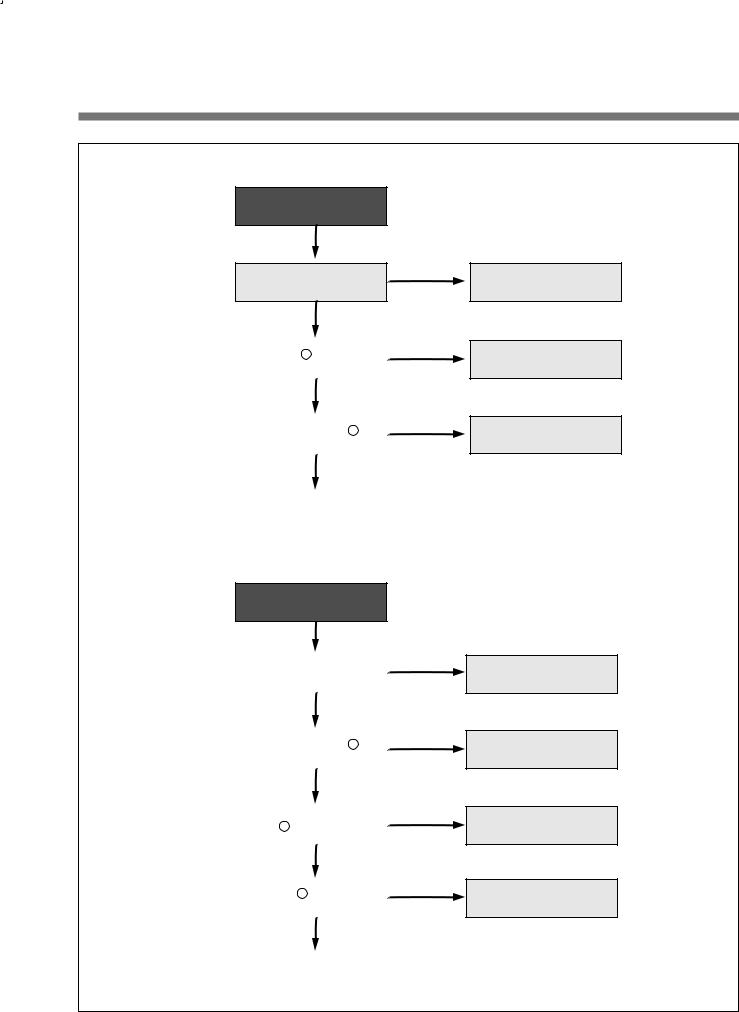
D.
Drum M/T loading stops.
NO
Is Motor 12V supplied?
YES |
|
|
NO |
Is pin 17 D.FG of |
|
IC601 supplied. |
|
|
|
YES |
|
|
NO |
Is pin D.PWM (pin 30 ) |
|
of IC601 supplied? |
|
|
|
YES |
|
|
|
Check connector |
|
and Motor. |
|
|
|
E.
Capstan M/T loading stops.
YES |
|
|
|
NO |
|
Is Motor 12V supplied? |
||
|
||
|
|
|
YES |
|
|
|
NO |
|
Is the input of pin 6 |
||
of PJ501 2V-3.5V? |
|
|
|
|
|
YES |
|
|
|
NO |
|
Is pin 4 of PJ50101 2.5V |
||
|
||
|
|
|
YES |
|
|
|
NO |
|
Is pin 31 (C.PWM) |
||
of IC601 Supplied? |
|
|
|
|
|
YES |
|
|
|
|
|
Check connector |
|
|
and Motor |
|
|
|
|
Check D606 of
power circuit.
Check C508, R510
Check IC601
Check power circuit.
Check circuit of R604, R605, R606.
Check R655, R656
Check IC601
9
F.
Drum M/T and Capstan M/T rotate at regular speed. (In REC mode)
NO |
|
|
|
NO |
|
Is C. Sync applied to |
Check C. Sync of |
|
pin 8 of IC601? |
|
VIDEO IC and Pattern |
|
|
|
YES
Check Motor.
G.
Emergency mode when plugging (Power cord)
Is EVER 5V supplied? |
NO |
|
Check power circuit. |
|
|
|
|
||
|
|
|
|
|
YES |
|
|
|
|
|
NO |
|
|
|
Does X601 crystal osciliate? |
|
Check IC601 and X601. |
|
|
|
|
|
||
|
|
|
|
|
YES |
|
|
|
|
|
NO |
|
|
|
Is CAM SW DATA Correct? |
|
Recheck connector |
|
|
|
|
|
||
|
|
and CAM SW contact. |
|
|
|
|
|
|
|
|
|
|
|
|
YES |
|
|
|
|
Check IC602.
 YES
YES
Check IC 601.
10
H.
Cassette is not inserted.
Is Motor 12V supplied?
YES
CAM DATA is changed when CST IN?
YES
Is 5V applied to
pin 4 of IC602 when CST IN?
YES
Chek IC602
NO |
Check D602 of power |
|
circuit |
|
|
NO |
Check connector. |
NO |
Check DECK part. |
|
|
||
|
|
|
|
NO |
Is 5V supplied at |
NO |
Check PATTERN |
|
|
||
|
pin 37 of IC601? |
|
|
|
|
|
|
|
|
|
|
|
YES |
|
|
|
|
|
|
|
Check IC601 |
|
|
|
|
|
|
11
I.
Power compensation does not operated.
When mains is unplugged is 3.6V at pin 21 and 64 of IC601?
 YES
YES
Is signal applied to pin 47 and 48 of IC601?
 YES
YES
Is 5V at pin 46 of IC601
YES
Check IC601
NO |
Check C602 |
|
NO
Check x601
NO |
Check reset circuit |
|
IC603 |
|
|
12
 Loading...